High-Contrast Electro-Optic Modulation of a Photonic Crystal Nanocavity by Electrical Gating of Graphene
Abstract
We demonstrate a high-contrast electro-optic modulation of a photonic crystal nanocavity integrated with an electrically gated monolayer graphene. A high quality () factor air-slot nanocavity design is employed for high overlap between the optical field and graphene sheet. Tuning of graphene’s Fermi level up to 0.8 eV enables efficient control of its complex dielectric constant, which allows modulation of the cavity reflection in excess of 10 dB for a swing voltage of only 1.5 V. We also observe a controllable resonance wavelength shift close to 2 nm around a wavelength of 1570 nm and a factor modulation in excess of three. These observations allow cavity-enhanced measurements of the graphene complex dielectric constant under different chemical potentials, in agreement with a theoretical model of the graphene dielectric constant under gating. This graphene-based nanocavity modulation demonstrates the feasibility of high-contrast, low-power frequency-selective electro-optic nanocavity modulators in graphene-integrated silicon photonic chips.
Graphene has intriguing optical properties and enables a range of promising optoelectronic devices Bonaccorso et al. (2010); Konstantatos et al. (2012); Mueller et al. (2010); Xia et al. (2009); Lemme et al. (2011); Liu et al. (2011); Bao et al. (2009); Sun et al. (2010); Hendry et al. (2010). To enhance the inherently weak light-matter interaction in this single atomic layer material, grahene has been coupled to optical waveguides and cavities Liu et al. (2011, 2012); Furchi et al. (2012); Engel et al. (2012); Gu et al. (2012). In the limit of wavelength-scale confinement, we recently demonstrated a dramatic enhancement of the light-matter interaction for graphene coupled to a planar photonic crystal (PPC) nanocavity, which reduced the cavity reflection by more than 20 dB Gan et al. (2012). Here, we employ this system to demonstrate a high contrast electro-optical modulation of the cavity reflection, in excess of 10 dB. The modulation is achieved by electrical gating of the graphene monolayer using an electrolyte, which, while slow, shows the fundamental capability of graphene-based modulation of nanocavities. Furthermore, we employ the strong coupling between the cavity modes and graphene for precision spectroscopy of graphene under gating conditions. We measure a complex dielectric constant that agrees with a theoretical model of the optical conductivity in graphene and supports the notion of residual absorption even when the Fermi level is tuned far above the transparency condition for infrared photons at energy , namely .

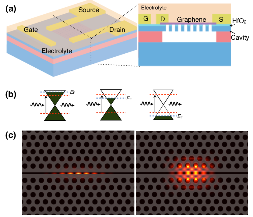
As shown in Fig.1(a), the experimental device consists of an air-suspended PPC cavity that is coupled to a graphene field effect transistor (FET) gated by a solid electrolyte Mak et al. (2009); Lu et al. (2004). The optical transmission of graphene for an incident photon with frequency is modulated by electrostatic tuning the graphene’s Fermi energy (). As shown in Fig. 1(c), when is tuned away from the Dirac point by more than half of the photon energy , the interband transitions are inhibited, reducing graphene absorption Wang et al. (2008); Li et al. (2008).
To improve the overlap between graphene and cavity resonant modes, we employ an an air-slot PPC nanocavity Gao et al. (2010) with strongly confined modes in the air-gap, as shown in Fig. 1(b). This design improves the graphene-optical mode coupling rate by approximately two-fold compared to inear three-hole defect cavities used previously Gan et al. (2012), where light is confined in the high index material Akahane et al. (2003) and therefore experiences less overlap with the graphene layer. The air-slot PPC nanocavities are fabricated on a silicon-on-insulator wafer with a 220 nm- thick silicon membrane, using a combination of electron beam lithography and dry/wet etching steps. We employ mechanically exfoliated graphene monolayers, which are transferred onto PPC nanocavities using a precision alignment technique Dean et al. (2010). The drain, source, and gate electrodes of the graphene FET are fabricated using electron beam lithography and titanium-gold electron beam evaporation. In previous experiments, we found that these contacts can gate the intrinsic or lightly doped silicon membrane directly and influence the cavity spectroscopy under doping. To avoid this, the devices described in this study include a conformal 10 nm hafnium oxide (HfO2) layer grown on the PPC using atomic layer deposition before the metal contacts are fabricated (see Figure 1(a)).
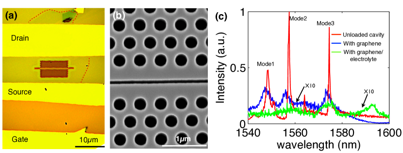
Figure 2(a) displays an optical image of one of the completed graphene-PPC nanocavity devices. The dashed red line indicates the boundary of the monolayer graphene, which is furthermore confirmed using micro-Raman spectroscopy. The gate electrode is about 15 m from the graphene flake to ensure effective doping through the electrolyte. Figure 2(b) shows a scanning electron microscope (SEM) image of the slot cavity with lattice spacing of nm and lattice hole-radii of nm. After graphene is transferred and contacted, we spin-coat electrolyte (PEO plus LiClO4) on the full wafer, which provides a high electric field and carrier density in graphene Mak et al. (2009); Lu et al. (2004), while also capping the device.

We characterize the graphene-PPC nanocavity using a cross-polarization confocal microscope with a broad-band (super-continuum laser) excitation source Gan et al. (2012); Englund et al. (2007). The reflection is analyzed using a spectrometer with resolution of 0.05 nm. The slot cavity has three dominant resonant modes Gao et al. (2010) at wavelengths of nm (Mode1), nm (Mode2), and nm (Mode3). As shown in Figure 2(c), the intrinsic cavity resonances first blue-shift upon HfO2 and graphene transfer, as expected for a decrease in the refractive index of the thin HfO2 layer during the annealing step of the graphene transfer process (see Supporting Information). The electrolyte has a real dielectric constant of that subsequently red-shifts the cavity J. D. Joannapolous, S. G. Johnson, J. N.Winn and Meade (2008), as shown in the green curve in Fig. 2(c). Modes 1 and 2 become indistinguishable after graphene and electrolyte deposition because they experience different red-shifts due to different overlap with the electrolyte (see Supporting Information).
Fitting the cavity resonances to Lorentzian curves, we estimate factors of for modes . After the single-layer graphene transfer, the factors decrease to 350, 640, and 440, respectively. Employing perturbation theory to the graphene-PPC system Gan et al. (2012), we obtain that the energy decay rates due to graphene absorption for these three resonant modes are , where are the resonant frequencies of the cavity modes. These loss rates indicate that the coupling between the graphene and mode3 is strongest, which is expected from the electric field distributions of the resonant modes: modes 1 and 3 have a strong optical fields — and therefore a large overlap with graphene —in the air-gap, while the overlap with the air slot is far weaker for mode 2. The single-layer graphene causes a strong (nearly 18 dB) reduction of the reflected intensity in the three resonant peaks. After electrolyte deposition, the factors of the resonances drop slightly to 300 and 420 for modes 1 and 3, respectively.

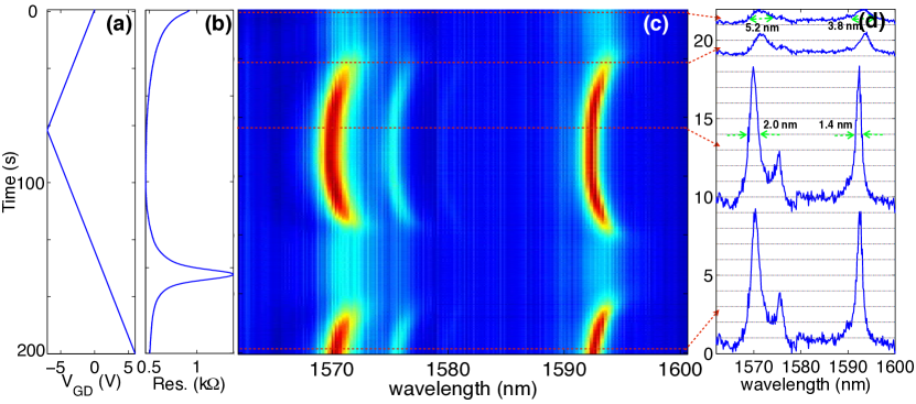
To study the electrical control of the graphene-PPC nanocavity, we measure the cavity reflectivity as a function of the gate voltage across the gate and drain electrodes. To aviod degradation of the electrolyte, the sample is measured in a chamber with vacuum of mbar at room temperature. The electrical signal through the drain and source is monitored simultaneously to record the doping level of graphene. Figure 3 shows the measurements of the electrical and optical signals as the gate voltage is linearly modulated. Here we scan at a speed of 0.1 V/s between -7 V — 6 V, as shown in Fig. 3(a). The measured resistance on the graphene FET in Figure 3(b) indicates a gate voltage for the charge neutral point at V. In these sweeps, the cavity reflection spectra are acquired continuously at frames of 33 ms each, as shown in Fig. 3(c). When is close to zero (-1 V¡ ¡0 V), the doping level on graphene is low. The cavity reflection is constant as that in the zero-bias condition, which is shown in the first panel of Fig. 3(d) with two resonant peaks at the wavelengths of 1571.7 nm and 1593 nm for modes 1 and 3, respectively. Tuning the graphene Fermi level by decreasing to -1 V, we observe that the two resonant peaks become narrower while red-shifting slightly, as shown in the second panel of Fig. 3(d). As the cavity loss is reduced, the cavity reflection intensity increases. Decreasing further, the resonant peaks grow and narrow sharply over a voltage range of V, while the center wavelengths blue-shift. Finally, the cavity linewidths and intensities saturate as drops below -2.5 V. However, the cavities continue to blue-shift over down to -7 V. The third panel of Fig. 3(d) shows the reflection spectrum at =-7 V. Because the peaks are now very narrow compared to the zero-bias case, the modes 1 and 2 again become distinguishable. We observe the reciprocal tuning phenomena when we increase back from -7 V to 0 V. For , the data show a wide flat spectrum () around the charge neutral point of graphene due to the low doping level. The fourth panel of Fig. 3(d) plots the spectrum at =6 V, showing the strong modulation of cavity reflectivity with the high electron side doping on graphene. The resonant peaks are increased to 8.5 when graphene is highly doped compared to zero-bias. Combining with the resonant wavelength shift, the modulation depth at is higher than 10 dB at the wavelenght of 1592.6 nm, which is the resonant wavelength of mode3 at =-7 V.
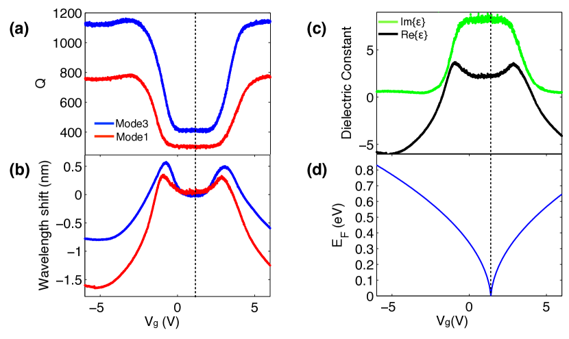
Fitting modes 1 and 3 in Fig. 3(c) to Lorentizan, we obtain the factors and resonant wavelengths as a function of from -6 V to 6 V. These are plotted in Figs. 4(a) and 4(b), respectively. For both cavity resonances, the changes of the factors and resonant wavelengths are symmetric with respect to . Due to the higher photon energy of mode1, its factor begins to increase after that of mode3. Both resonant modes show the saturation of the factor with the change from 300 (420) to 780 (1150) for mode1 (3). Figure 4(b) depicts the initial resonant wavelength red-shift, followed by the mode blue-shift, with a maximum change of 2 nm and 1.3 nm for modes 1 and 3, respectively.
The observed changes of factors and resonant wavelength shifts are due to the change of the complex dielectric constant of graphene Gan et al. (2012). We can calculate these changes from a knowledge of the overlap of the cavity modes with the graphene layer and using perturbation theory Gan et al. (2012). The results calculated from mode1 are shown in Fig. 4(c). The imaginary part of the graphene dielectric constant has a value of 8.2 at . It decreases to the minmum at =3 V, corresponding to eV, without any change even under higher . The real part of the graphene dielectric constant increases monotonically first from 2.1 at the charge neutral point to the maximum value of 3.6 at =1.4 V. Then it decreases to -5.9 continusly under the highest doping level. Figure 4(d) displays the calculated Fermi level on the graphene sheet as a funtion of . The obtained complex dielectric constant of graphene from the experiment measurements matches with theeoretical predictions Lu and Zhao (2012).

In conclusion, we have demonstrated that by coupling electrically gated graphene to a PPC nanocavity, it is possible to realize strong optical modulation . This finding shows great promise for future electro-optic chip-integrated, small-footprint modulators that employ doping graphene as the active medium. In future studies, graphene can be back-gated using highly doped silicon PPC cavity or dual graphene layers to increase the modulation into the GHz regimes Liu et al. (2011, 2012). Because of the high mobility and small capacitance of such PPC-graphene devices, we also anticipate low power consumption. The cavity enhancement also enabled the precise measurement of the graphene conductivity in a deep sub-wavelength region of graphene-mode overlap. The cavity therefore enable precision spectroscopy in small graphene volumes.
Acknowledgement: Financial support was provided by the Air Force Office of Scientific Research PECASE, supervised by Dr. Gernot Pomrenke and by the National Science Foundation through grant DMR-1106225. Fabrication of the PPC was carried out at the Center for Functional Nanomaterials, Brookhaven National Laboratory, which is supported by the U.S. Department of Energy, Office of Basic Energy Sciences, under Contract No. DE-AC02-98CH10886. Device assembly, including graphene transfer, and characterization was supported by the Center for Re-Defining Photovoltaic Efficiency Through Molecule Scale Control, an Energy Frontier Research Center funded by the U.S. Department of Energy, Office of Science, Office of Basic Energy Sciences under Award Number DE-SC0001085.
References
- Bonaccorso et al. (2010) F. Bonaccorso, Z. Sun, T. Hasan, and A. C. Ferrari, Nature Photonics 4, 611 (2010), ISSN 1749-4885, URL http://www.nature.com/doifinder/10.1038/nphoton.2010.186.
- Konstantatos et al. (2012) G. Konstantatos, M. Badioli, L. Gaudreau, J. Osmond, M. Bernechea, F. P. G. de Arquer, F. Gatti, and F. H. L. Koppens, Nature Nanotechnology 7, 363 (2012), ISSN 1748-3387, URL http://www.nature.com/doifinder/10.1038/nnano.2012.60.
- Mueller et al. (2010) T. Mueller, F. Xia, and P. Avouris, Nature Photonics 4, 297 (2010), ISSN 1749-4885, URL http://www.nature.com/doifinder/10.1038/nphoton.2010.40.
- Xia et al. (2009) F. Xia, T. Mueller, Y.-M. Lin, A. Valdes-Garcia, and P. Avouris, Nature nanotechnology 4, 839 (2009), ISSN 1748-3395, URL http://www.ncbi.nlm.nih.gov/pubmed/19893532.
- Lemme et al. (2011) M. C. Lemme, F. H. L. Koppens, A. L. Falk, M. S. Rudner, H. Park, L. S. Levitov, and C. M. Marcus, Nano letters 11, 4134 (2011), ISSN 1530-6992, URL http://www.ncbi.nlm.nih.gov/pubmed/21879753.
- Liu et al. (2011) M. Liu, X. Yin, E. Ulin-Avila, B. Geng, T. Zentgraf, L. Ju, F. Wang, and X. Zhang, Nature 474, 64 (2011), ISSN 1476-4687, URL http://www.ncbi.nlm.nih.gov/pubmed/21552277.
- Bao et al. (2009) Q. Bao, H. Zhang, Y. Wang, Z. Ni, Y. Yan, Z. X. Shen, K. P. Loh, and D. Y. Tang, Advanced Functional Materials 19, 3077 (2009), ISSN 1616301X, URL http://doi.wiley.com/10.1002/adfm.200901007.
- Sun et al. (2010) Z. Sun, T. Hasan, F. Torrisi, D. Popa, G. Privitera, F. Wang, F. Bonaccorso, D. M. Basko, and A. C. Ferrari, ACS Nano 4, 803 (2010), ISSN 1936-0851, URL http://pubs.acs.org/doi/abs/10.1021/nn901703e.
- Hendry et al. (2010) E. Hendry, P. Hale, J. Moger, A. Savchenko, and S. Mikhailov, Physical Review Letters 105, 097401 (2010), ISSN 0031-9007, URL http://link.aps.org/doi/10.1103/PhysRevLett.105.097401.
- Liu et al. (2012) M. Liu, X. Yin, and X. Zhang, Nano letters 12, 1482 (2012), ISSN 1530-6992, URL http://www.ncbi.nlm.nih.gov/pubmed/22332750.
- Furchi et al. (2012) M. Furchi, A. Urich, A. Pospischil, G. Lilley, K. Unterrainer, H. Detz, P. Klang, A. M. Andrews, W. Schrenk, G. Strasser, et al., Nano letters 12, 2773 (2012), ISSN 1530-6992, URL http://www.pubmedcentral.nih.gov/articlerender.fcgi?artid=3396125&tool=pmcentrez&rendertype=abstract.
- Engel et al. (2012) M. Engel, M. Steiner, A. Lombardo, A. C. Ferrari, H. V. Löhneysen, P. Avouris, and R. Krupke, Nature communications 3, 906 (2012), ISSN 2041-1723, URL http://www.ncbi.nlm.nih.gov/pubmed/22713748.
- Gu et al. (2012) T. Gu, N. Petrone, J. F. Mcmillan, A. V. D. Zande, M. Yu, G. Q. Lo, D. L. Kwong, J. Hone, and C. W. Wong, Nature photonics 43, 1 (2012).
- Gan et al. (2012) X. Gan, K. F. Mak, Y. Gao, Y. You, F. Hatami, J. Hone, T. F. Heinz, and D. Englund, Nano letters (2012), ISSN 1530-6992, URL http://www.ncbi.nlm.nih.gov/pubmed/23043452.
- Mak et al. (2009) K. Mak, C. Lui, J. Shan, and T. Heinz, Physical Review Letters 102, 100 (2009), ISSN 0031-9007, URL http://link.aps.org/doi/10.1103/PhysRevLett.102.256405.
- Lu et al. (2004) C. Lu, Q. Fu, S. Huang, and J. Liu, Nano Letters 4, 623 (2004), ISSN 1530-6984, URL http://pubs.acs.org/doi/abs/10.1021/nl049937e.
- Wang et al. (2008) F. Wang, Y. Zhang, C. Tian, C. Girit, A. Zettl, M. Crommie, and Y. R. Shen, Science (New York, N.Y.) 320, 206 (2008), ISSN 1095-9203, URL http://www.ncbi.nlm.nih.gov/pubmed/18339901.
- Li et al. (2008) Z. Q. Li, E. a. Henriksen, Z. Jiang, Z. Hao, M. C. Martin, P. Kim, H. L. Stormer, and D. N. Basov, Nature Physics 4, 532 (2008), ISSN 1745-2473, URL http://www.nature.com/doifinder/10.1038/nphys989.
- Gao et al. (2010) J. Gao, J. F. McMillan, M.-C. Wu, J. Zheng, S. Assefa, and C. W. Wong, Applied Physics Letters 96, 51123 (2010), URL http://link.aip.org/link/?APL/96/051123/1.
- Akahane et al. (2003) Y. Akahane, T. Asano, B.-S. Song, and S. Noda, Nature 425, 944 (2003).
- Dean et al. (2010) C. R. Dean, A. F. Young, I. Meric, C. Lee, L. Wang, S. Sorgenfrei, K. Watanabe, T. Taniguchi, P. Kim, K. L. Shepard, et al., Nature nanotechnology 5, 722 (2010), ISSN 1748-3395, URL http://www.ncbi.nlm.nih.gov/pubmed/20729834.
- Englund et al. (2007) D. Englund, A. Faraon, I. Fushman, N. Stoltz, P. Petroff, and J. Vuckovic, Nature 450, 857 (2007).
- J. D. Joannapolous, S. G. Johnson, J. N.Winn and Meade (2008) J. D. Joannapolous, S. G. Johnson, J. N.Winn and R. D. Meade, Princeton University Press (2008), URL http://onlinelibrary.wiley.com/doi/10.1002/cbdv.200490137/abstract.
- Lu and Zhao (2012) Z. Lu and W. Zhao, Journal of the Optical Society of America B 29, 1490 (2012), ISSN 0740-3224, URL http://www.opticsinfobase.org/abstract.cfm?URI=josab-29-6-1490.
- Mikhailov and Ziegler (2007) S. Mikhailov and K. Ziegler, Physical Review Letters 99, 1 (2007), ISSN 0031-9007, URL http://link.aps.org/doi/10.1103/PhysRevLett.99.016803.
- Majumdar et al. (2012) A. Majumdar, J. Kim, J. Vuckovic, and F. Wang, arXiv 1210.6716, 1 (2012).