Edge electrostatics revisited
Abstract
In this work we investigate in detail, the different regimes of the pioneering work of Chklovskii et al [1], which provides an analytical description to model the electrostatics at the edges of a two-dimensional electron gas. We take into account full electrostatics and calculate the charge distribution by solving the 3D Poisson equation self-consistently. The Chklovskii formalism is reintroduced and is employed to determine the widths of the incompressible edge-states also considering the spin degree of freedom. It is shown that, the odd integer filling fractions cannot exist for large magnetic field intervals if many-body effects are neglected. We explicitly show that, the incompressible strips which are narrower than the quantum mechanical length scales vanish. We numerically and analytically show that, the non-self-consistent picture becomes inadequate considering realistic Hall bar geometries, predicting large incompressible strips. The details of this picture is investigated considering device properties together with the many-body and the disorder effects. Moreover, we provide semi-empirical formulas to estimate realistic density distributions for different physical boundary conditions.
keywords:
Quantum Hall effect, Edge statesPACS:
73.43.-f , 73.23.-b , 73.43.Cd1 Introduction
Cooling a high-mobility two-dimensional electron system (2DES) near absolute zero and subjecting the system to strong perpendicular magnetic fields , results in quantized Hall resistances when magneto-transport measurements are performed. This phenomena is called the quantized Hall effect (QHE) [2]. The quantized Hall resistivity and longitudinal resistivity are often explained as a result of Landau quantization at high magnetic fields. Quantized levels are called Landau levels (LLs) which are highly degenerate, and the energy of the LLs are given by , where is the level index, is Planck’s constant and represents the cyclotron frequency of an electron with an effective mass ( for GaAs/AlGaAs heterostructures).
After the discovery of QHE, considerable attention is diverted to the unexpected transport properties of 2DESs. The current transport in a 2DES is usually described by two main pictures, namely the bulk [3] and the edge pictures [1, 4, 5, 6]. In the bulk picture one assumes an infinite homogeneous 2DES, where the current flows from the bulk. Transport properties are essentially determined by impurity scattering and localization arguments are dominant [3]. Conversely, in the edge picture a finite system is considered and the current is assumed to be confined near the edges of the sample. The transport is mainly due to back-scattering suppressed, one dimensional ballistic channels. The properties of these channels are widely investigated in many context [7, 8, 9]. However, if one takes into account the direct Coulomb interactions the 1D channel picture is modified. Due to the presence of a perpendicular magnetic field, the 2DES has a peculiar density of states (DOS) distribution as a function of energy (and position). The peculiarity of the DOS result in unusual screening properties [1, 10, 11]. Such that, if the Fermi level falls between two adjacent LLs, electrons cannot be redistributed. Therefore, they do not contribute to screening locally. The region exhibiting poor screening properties is called incompressible and it behaves like an insulator. For further references, it is useful to define a dimensionless parameter: The filling factor , where and are the number densities of the electron and the magnetic flux for a given area , respectively. The local filling factor , measures the number of fully occupied Landau levels (locally), where and denote the coordinates in real space. Here it is assumed that the field is homogeneous both in space and time. Therefore, if the region is incompressible, the filling factor equals to an integer. Whereas, if the Fermi level is pinned to one of the Landau levels, i.e. the level is partially occupied ( non-integer), electrons can be redistributed. Hence, the region is compressible and it behaves like a metal. Starting from late 80’s, the formation of these peculiar strips have been investigated theoretically, considering different approaches and approximations. One of the most appreciated scheme is the so-called Chklovskii picture [1], where a Thomas-Fermi mean field approximation is considered to obtain electrostatic properties of the 2DES at the edges of the system in a non-self consistent manner at zero temperature [1, 12]. Subsequently, K. Lier and R. R. Gerhardts have investigated the properties of these strips at finite temperatures, performing self-consistent (SC) calculations [13]. In this work, the deviations from the Chklovskii picture are already shown both in spatial distribution and in calculation of the widths of the strips. Afterwards, it is shown that the incompressible strips are much narrower than the predictions of the pioneering work [14], considering the effects resulting from the growth directions. The reports mentioned above are all based on the Thomas-Fermi approximation, which explicitly assumes that the overall potential profile varies slowly on the quantum mechanical length scales, e.g. on the scale of the wave length. Hence, the finite width of the wave functions is neglected and quantum mechanical properties of the electrons are ignored such as finite tunneling rates etc. However, if an incompressible strip is formed, a strong potential variation exists, therefore, if the strip width becomes comparable with the wave extent, TFA becomes questionable [6], which we also address in the present work. The first order quantum mechanical effects were included to the self-consistent calculations within a mean-field Hartree approximation, where the results show that the incompressible strips vanish in certain magnetic field intervals [6, 15]. These results have important consequences on the transport taking place at the 2DES both theoretical [16] and experimental wise [17, 18].
In this paper, we investigate the non-self-consistent Thomas-Fermi approach of Chklovskii, Shklovskii and Glazmann (CSG) in detail to clarify the effects stemming from experimental conditions. For this purpose, the electron density distribution and the widths of incompressible strips are calculated self-consistently considering different sample preparation conditions, namely by gates, by chemical etching processes and a superposition of these procedures. We first summarize the analytical approach of the mentioned work and clearly state the assumptions made. In the next step, we present the results of a fully self-consistent calculation performed on a 3D crystal and compare the electron densities with the analytical results. Utilizing the CSG formalism the widths of the incompressible strips are calculated also considering spin degree of freedom, disorder and quantum mechanical effects. In this work, we explicitly show that more than one incompressible strip with different filling factors cannot form at typical Hall bar geometries due to the steepness of the total potential at the edges. In a final section, we discuss the different regimes of the edge profiles considering gated, etched and trench gated samples.
2 The Edge-states
Since the quantized Hall effect is related to the existence of the “edge-states”, it is useful to clarify the definition of these states at different pictures, while the notation becomes confusing for a non-expert. One first encounters the notation edge-states in an early work by Halperin [4], where he discusses finite size effects arising from the real sample structure, i.e. the confinement potential. Such an approach is fairly different than the conventional bulk picture, which neglects the boundary effects all together [3, 19] and attributes the quantized Hall effect to gauge invariance and localization of the electronic states. Even a brief discussion of the bulk theory, hence localization picture, is far beyond the scope the present work. Therefore, we avoid such a discussion. However, the basic idea in a superficial manner is to localize electrons to bulk states due to disorder. Hence, these electrons cannot contribute to transport and therefore the Hall conductance is quantized whereas, the longitudinal conductance vanishes.
2.1 The Halperin and Landauer-Büttiker type edge-states
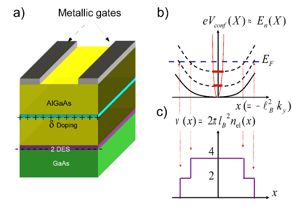
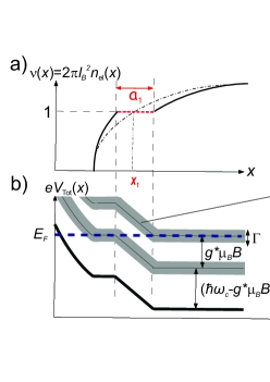
In contrast with the bulk picture, one neglects the disorder effects and considers the finite size of the system instead, it is observed that the single particle Landau levels are bent at the edges due to the confinement potential. Fig. 1(a) presents a typical crystal structure and Fig. 1(b) shows the confinement due to the remote (homogeneous) donors (thick black curve) and the magnetic confinement of a single particle (broken lines) together with the position dependent Landau levels (red lines following the confinement potential). Such a plot corresponds to the single particle Hamiltonian given as,
| (1) |
where we assume a translational invariance in direction and consider the Landau gauge to define the field in the direction, i.e. . Note that the horizontal axes in Fig. 1(b)-(c) are both in real and momentum spaces, where the center coordinate is related to by , and is the magnetic length. Here, is the quasi-continuous momentum in direction. The crucial assumption to have such an energy dispersion is to have a smooth confinement potential, hence, one can replace the dependent energy eigenvalues by a constant given by the local value of the confinement potential (energy), i.e. . This enables us to fix the spatial (and energetic) distribution(s) of the edge-states for a given Fermi energy , (dark) dashed horizontal broken line. When it comes to transport, it is easy to conclude that the current is carried by the edge-channels while there are available states at the Fermi energy once cuts through the Landau levels. At equilibrium, the number of edge channels carrying positive momentum (namely forward movers) equals to number of channels carrying negative momentum (namely backward movers) and as a result of every channel can only carry a unit of conductance (the velocity is canceled due to the density of states in 1D), net current is zero. To impose a finite current, one has to increase the chemical potential energy of forward movers by an amount of , hence the potential (energy) difference between the probe (side) contacts is now quantized to the number of edge channels. A detailed description can be found in Ref. [20]. [Such a transport scheme is highly out of equilibrium, since one injects electrons which have considerably higher energies than the electron sea, and the unoccupied states carry the non-equilibrium excess current.] Moreover, the injected electrons do not induce a Hall potential which is spread across the sample; the spatial distribution of the electrochemical potential is overlooked and the results deviate strongly from the experimental findings [21, 22]. The above formalism is known as the Landauer-Büttiker (LB) picture [5], and these edge-states are named as (1D and ballistic) Landauer-Büttiker edge states (LBES). Since we neglected disorder and the bulk of the sample is completely incompressible, as a result, no back-scattering can take place, therefore the longitudinal resistance vanishes which is accompanied by the quantized Hall resistance. However, such a picture is not adequate to explain the transitions between the quantized Hall plateaus observed experimentally. Hence, one should allow some scattering due to the impurities and introduce bulk states, where electrons are orbiting around hills and valleys of the disorder potential. Such a description is so far so good only if one can bare the fact that the resulting electron density distribution is stepwise and highly unstable (see Fig. 1(c)), due to the strong Coulomb force between electrons. In fact, chronologically, Halperin introduced the concept of “edge-states” even earlier than the mentioned work above [4]. However, there the edge-states are obtained for a system which presumes infinite walls at the physical edges of the system. For such a system, the solution of the Schrödinger equation can be obtained analytically. The wave functions are described by parabolic cylindrical functions, whereas the Landau levels depending on the center coordinate are only bent at the edges, in contrast to LB picture where potential varies smoothly in the scale of . An important implication of such infinite walls is that the energy dispersion in no longer equidistant, . Utilizing Bohr-Sommerfeld quantization one can obtain the dispersion at the edges [23] or by considering WKB approximation one has [24]
| (2) |
Hence, equidistant quantization at the bulk, i.e far from the infinite walls, is recovered.
It is important to emphasize that, the approach of Halperin is rather different than the Büttiker one, in the first case infinite walls are assumed at the edges and the eigenfunctions satisfy the condition and the external potential is zero in the bulk. In the latter case, the external potential varies smoothly and the eigenfunctions satisfy . Clearly, these two approaches assume different boundary conditions and impose different criteria on the external potential.
2.2 The Chklovskii edge-states
The discrepancy due to the stepwise behavior of the density profile is cured, if one includes the classical electron-electron interactions (direct Coulomb), which was discussed even earlier than Chklovskii et al by R. R. Gerhardts and his co-workers [10, 25] and by A. M. Chang [26]. However, we focus our discussion on the elegant analytical investigation of Chklovskii et al. They studied the electrostatics of the edge channels and provided an analytic expression for the widths of the incompressible strips depending on the filling factor. In their work, 2DES is considered to be formed in a heterostructure (in fact in their work the 2DES is formed at the interface of a semiconductor and air), where the fluctuations at the donor concentration is neglected and the donor density set equal to electron density far from the boundaries. They create the boundary of 2DES by applying a negative voltage to the metallic gate on the surface assuming a half-plane geometry. The solution assumes a translational invariance in the direction. The gate potential determines the width of depleted strip () and is given by
| (3) |
where is the surface number density of the homogeneous donor layer. In this model a capacitor is considered where metallic plates are in the same () plane together with the donor and electron layers. The metal plates are assumed to be separated from each other by an uniformly charged insulator. One of the metal plates is exposed to a negative gate potential and the other metal plate is considered as grounded. Thus, the gate potential pushes the electrons to the grounded plate where the 2DES is formed. Since, the half-space is occupied by a semiconductor with a high dielectric constant () the Laplace equation can be solved. As a result, they have obtained the following equation for the spatial distribution of the electron density in the metallic like strip begins at the end of the depletion region:
| (4) |
which reaches to its bulk value far away from the boundary. Note that the electron density given by the above equation is eligible in the absence of magnetic field, only considering in-plane gates which reside at the plane of 2DES.
Next, they consider single particle interactions in 2DES and the ladder like behavior is replaced by smoother density distribution that present narrow constant density regions, i.e incompressible strips. They propose that co-existing (and adjacent) compressible and incompressible regions are formed in the presence of strong magnetic fields. They assume that the compressible regions behave like a metal so screening is perfect and electrostatic potential is completely constant, whereas in the incompressible regions, screening is very poor and the system behaves like an insulator. As a result of analytic calculations, they derived the generalized expression for the strip widths assuming any integer number :
| (5) |
where is the derivative of electron density with respect to spatial coordinate calculated at the center of the strip, i.e at , and the single particle energy gap is denoted by . It is very important to note that, a perfect metal is assumed for the compressible regions ( non-integer, ) and a perfect insulator is assumed for the incompressible strips ( integer, ), such an assumption cannot be justified for a 2DES which is formed at the interface of two semiconductor materials for sure. A simple calculation of the screened potential
| (6) |
for a given external potential via dielectric function
| (7) |
together with the constant density of states () of a 2D system already shows that, if the is not infinite (like in a metal), such an approximation fails. These compressible and incompressible strips are known as the Chklovskii edge-states, which are no longer 1D channels. However, as we discuss later once more, the vanishing longitudinal resistance is attributed to the absence of backscattering and one obtains the quantized Hall plateaus simply by counting the number of compressible strips. Hence, 1D LB edge states are replaced by current carrying compressible strips, separated by insulating incompressible strips that suppress back-scattering.
In the original work, spin degree of freedom is neglected, hence, the energy gap equals to . Therefore, all integer (odd or even) filling factors assume the same energy gap. However, in our calculations, we consider spin splitting in a rather phenomenological manner and take into consideration Zeeman splitting by assuming an enhanced effective Lande- factor. Actual value of -factor depends on whether exchange component of Coulomb interaction is taken into account or not. Since the exchange interaction depends on the spin polarization of the system, -factor varies depending on the magnetic field. Enhancement of effective factor is already investigated by Manolescu and Gerhardts [27] almost two decades ago and it has been shown that local spin polarization leads to wider spin polarized incompressible strips due to spatially enhanced Zeeman gap. However, here for simplicity we assume that factor does not depend on . Since at the magnetic field intervals we are interested in, the incompressible stripes are already narrow and spin polarization becomes small, the effective Zeeman splitting will become less significant therefore dependency of will bring only small quantitative corrections. For a detailed study of spin effects on incompressible strips we refer to a recent spin density functional theory calculation considering bulk [28, 29] and predicting collapse of the Zeeman gap due to small . Moreover, under typical experimental conditions (e.g. =1 K, =5 T and low-mobility samples), the gap already closes and the odd incompressible strip disappears. However, due to exchange-correlation effects it is explicitly shown that the incompressible strips are indirectly enhanced [28, 29]. In principle one can fit the factor using the widths of odd incompressible strips from the experiments [17, 21]. This experiments showed that exchange and correlation effects enlarge the energy gap of the LLs which corresponds to odd filling factor as if the factor value is similar to . However, since our aim is to show qualitatively that the odd (also even) integer incompressible strips collapse due to the strength of the confinement potential, we use a constant , which nevertheless describes the system properly.Therefore, if one takes into account the Zeeman splitting, the energy gaps are given as
| (8) |
Another handicap of the Chklovskii model is due to the considered geometry, namely the half-plane, which is cured in the subsequent work [12]. However, the 2DES, gates and donors reside on the same plane; but this is not reasonable for a gated and shallow etched defined realistic samples. As an exception, deep etched samples can still be approximated by the Chklovskii model in calculating the strip positions, if the gate potential is set to -0.75 V, corresponding to mid gap energy of GaAs. However, the widths are usually over estimated [6, 17]. In our calculations, we consider a sample which has the dimensions of a m m unit cell, where side contacts also have realistic dimensions ( nm in width and nm in length, residing on both sides). 3D Poisson equation is solved self-consistently for this geometry (see Fig. 1(a)), using the successful 4th order grid technique. In three dimensions, evaluating both the potential and charge densities comparatively is the essence of 4th order grid technique [30]. At this technique, initial potential (gate potential) and charge (donor) density are given for a grid point, and using Poisson equation, the nonuniform potential on the outer boundary (due to the geometry) and charges are iteratively calculated on the nearest neighbors grid points. This technique is implemented to many other similar structures [30, 31, 32]. Thus, we numerically obtain the electron density and total electrostatic potential distributions for a given crystal structure and lithographic pattern. By applying different gate voltages to the metallic gates and changing the etching depths of the structure we control the electron density distribution and also manipulate the depletion length.
2.3 Full electrostatics of the crystal
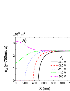
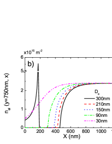
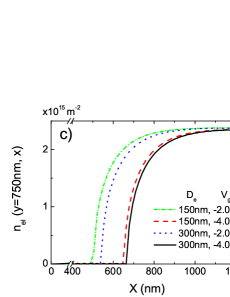
In this section we show the results of our self-consistent calculations, considering gate, etched and trench gated structures while varying the depth of the 2DES and etching together with the gate potentials. The main outcomes of our simulations are presented in Fig. 2, where we show the electron density distribution as a function of lateral coordinate considering a gate defined structure (a), an etched sample (b) and a trench gated sample (c). The extent of depleted regions is manipulated by applying different gate potentials and/or etching depths. Fig. 2(a) presents density variation for typical gate potentials, note that the gates are at the surface and the surface potential is pinned to the mid gap of GaAs, i.e. V. Therefore, zero gate potential (double doted-dashed curve) behaves as a positive potential, relative to the surface, hence more electrons are accumulated beneath the gate. This is the first difference between our 3D calculations and the in-plane gated Chklovskii geometry, there even a small gate voltage generates a depleted strip. In contrast, we can obtain the pinch-off voltages of the gates in a self-consistent manner. The first negative potential bias is V (note that this value is effectively -.25 V), where the density of the 2DES starts to be reduced below the gates. Only if a larger negative potential is applied to the gates, one observes an electron depleted region (dotted line) V, with a depletion length of nm. One can clearly see from the gate potential dependence that the does not scale linearly with the applied gate voltage as assumed in equation (3). In our calculations, we consider a heterostructure geometry as shown in Fig. 1(a). The total hight of the sample is 440 nm, where the 2DES lies 288 nm below the surface and the delta doped donors are located 165.5 nm below. Next, we consider the etching defined samples. We investigate the electron density distributions of the sample for varying etching depths () and the results are showed in Fig. 2(b). If a tiny layer is removed from the surface (i.e. nm, double dotted-dashed pink line) no electron depleted region occurs, likewise the low gate bias. Once the etching depth becomes larger than nm, an electron depleted strip forms. However, note that the width of the depleted region is much larger when compared to the gated sample. One can observe that the etched sample in Fig. 2(b) the electron density changes with etching depths, as expected. Most interestingly, if one etches the crystal below the 2DES layer ( nm, black solid line), side surface charges become visible. This is the regime where analytical calculations of Gefland and Halperin [33] fit better to the numerical results. These side charges push the 2DES even stronger than an in-plane gate, since they are spread all over the side surface. Another way to define narrow constrictions is the so-called trench gating. Here, first some layer of crystal is removed starting from the surface and then the metallic gate is deposited to this etched region. Of course, this procedure is much more complicated than either by gating or etching, however, has the advantage to generate steeper confinement potentials due to etching, and also one can control this steepness by applying a potential on the trench gates. Such structures are preferred usually in interference devices [34, 35], since a full control of the transmission parameters are necessary [32]. Fig. 2(c) depicts the resulting electron density considering trench gated samples, which leads wider depleted regions compared to other boundary defining techniques. Applying negative gate voltages to the etched sample, pushes the (side) surface charges to the bulk of the sample and the peak in the Fig. 2(b) vanishes, since now the side charges are captured by the metallic gates. It is apparent that the derivative of the density profile (i.e. the slope) is much larger than the gated structures, hence, according to the equation (5) the resulting incompressible strip will be much narrower compared solely defined by gates.
In a next step, we also investigated various electron layer depths from the surface (), while also varying the donor layer depth from the surface (), as shown in Fig. 3, while fixing the gate potential or etching depth.
The first observation is that the distance between the surface and the electron layer effects the bulk electron density considerably. Once the electron layer is further away from the surface, i.e. the gates, the electron density increases almost exponentially, since the electrostatic potential decreases rapidly with the distance. As an important note, we point that the gate defined edges provide a smoother potential profile near the physical boundaries of the sample when compared to etch defined samples. By performing calculations considering various depths of the 2DES and the donor layer we provide the following empirical formula to estimate the depletion length:
| (9) |
where is a normalization constant that that depends on the applied gate potential given by condition, whereas is a dimensionless constant as a free fit parameter.
Another important conclusion that can be made from our self-consistent calculations is that larger gate potentials essentially yield steeper confinement at the edges. Performing a suitable fitting results in the following form of the electron density
| (10) |
where determines the electron poor region width just in front of the gate and is a parameter related with the slope of electron density. We observed that is the order of for smooth electron density, consistent with the non-self-consistent calculations.
We also performed a similar fitting process to the etched defined samples, where the non-linear relation between etching depth and depletion length is observed once more. Interpolating the relation between the etching depth and depletion length over various sample parameters yield the form
| (11) |
where the constant is calculated as . A similar density profile given in equation (10) fits perfectly to our self-consistent results.
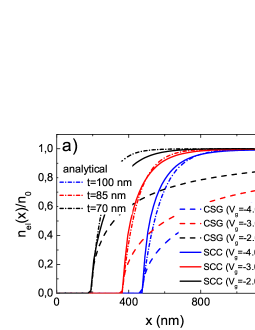
This is shown in Fig. 4, where the density profiles are calculated using the self-consistent scheme (solid lines), the empirical formula - Eq. 10 (dash-dotted) and the analytical formula provided by Chklovskii et al, i.e. Eq. 4 (dashed line). One observes fairly good overlap between the self-consistent calculations and Eq. 10, whereas the Chklovskii prediction fails by a gross amount, both qualitatively and quantitatively.
So far we have shown by solving the full electrostatics that, the analytical non-self-consistent Thomas-Fermi approach predicts rather different density profiles compared to our results. Now the question is how important are these deviations? In fact, when calculating the strip widths, these differences become much more emphasized, since the widths () strongly depend on the derivative of the electron density. Next we present our numerical results calculated within the Chklovskii picture, which show that co-existence of many incompressible strips with different integer filling factors are barely possible.
2.4 Strip widths
Once the electron density distribution is obtained from electrostatics, it is an easy task to locate the center of the strip for a given by the relation and the width of the strip from Eq. (5), as shown in Fig. 5(a) for . Here the thin curve depicts the electron density distribution when magnetic field is absent. Fig. 5(b) represents the potential energy distribution as a function of position. As depicted in Fig. 5(b) one observes a potential drop when incompressible strip is formed.
Similar to Chklovskii’s analysis, however, utilizing the self-consistently obtained electron density distribution (Eq. 10), we obtain the following expression to determine the widths of the incompressible strips
| (12) |
where and corresponds to incompressible strip widths of and , respectively and , are the dimensionless energy parameters. In Fig. 6, we show the widths of the incompressible strips as a function of magnetic field calculated within the Chklovskii formalism and our self-consistent calculations.
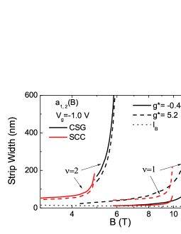
For the moment we neglect the finite temperature effects and calculate and depending on the field strength while considering a gate defined sample under the -1.0 V gate bias with m-2 donor concentration. Note that, at this voltage, the 2DES is still not depleted and the electron density varies smoothly. In Fig. 6, we see the incompressible strips widths obtained within the CSG picture [1] (black curves) and our SCC calculations (red curves). We calculate the incompressible strips with two different factors. As mentioned before, we consider either the bulk factor or an exchange enhanced one (taken to be 5.2, similar to the experimental values [36]). Although in our sample, the incompressible strips widths which are calculated by SCC are finite with increasing magnetic field, the strip widths increase unrealistically within the CSG calculation, since a half-plane geometry is assumed in the latter work. The real samples as our sample assume boundaries which take the electron density in a finite region. We see that, the Chklovskii picture yields artificially wide strips due to the incorrect modeling of the density profiles both for and 5.2. Ihnatsenka and Zozoulenko are compared the results of Chklovskii et al and their density functional theory calculations considering the formation of the compressible strips [37], where it is shown that strip widths are narrower than CSG picture. Apparently, our results are considerably more consistent with Ref. [37] (cf. Fig. 6).
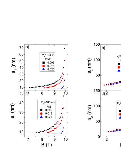
In a final investigation, we calculate the magnetic field dependency of the incompressible strips also considering the effects due to collision broadening, Fig. 7. We included the effect of disorder via density of states broadening, however, the effect of long-range potential fluctuations stemming from impurities is neglected. This can be justified, if one considers a high-mobility system. Whereas, the low-mobility samples can also be modeled within the screening theory once the long-range fluctuations are included to the self-consistent scheme [38]. We see that incompressible strips do not exist in all magnetic fields, since the gap collapses due to scattering broadening. The critical magnetic field value that the incompressible strip collapses is determined by the electron density, gate voltage, etching depth etc. The odd incompressible strips widths are narrower compared to even incompressible strips widths and it stems from the fact that the Zeeman gap is small compared to the Landau gap, if exchange effects are neglected. The incompressible strip forms in magnetic field interval T, whereas incompressible strip is formed in magnetic field interval T. We see that stronger disorder results in a narrower incompressible strip. At , , disorder energies the incompressible strip cannot form, whereas while incompressible strip is present. It is clear that the effect of disorder is much more crucial for the odd integer filling factors. Numerically, we find that to observe an incompressible strip assuming the disorder potential strength must be lower than , whereas for this value is changed to . Basically, disorder broadens the density of states and when disorder potential leads the wave functions to overlap on both sides of the incompressible strip, essentially the incompressible strip vanishes.
3 Conclusions
We investigated the details of Chklovskii et al [1] picture by taking into account the full electrostatics of the samples. By considering the device properties, e.g. geometry, disorder, confinement, boundary conditions also taking into account many body and disorder effects, qualitatively, it is shown that the estimations of the non-self-consistent picture is strongly limited. Instead, by performing self-consistent calculations, we derived semi-empirical formulas for realistic electron density distributions utilizing a 3D numerical algorithm. In addition, the variation of the depletion lengths is studied considering etched and gate defined samples. We observed that, the linear gate voltage-depletion length dependency assumed in Ref. [1] is not justified. It is also found that the etch and the gate defined samples present fairly different profiles compared to existing literature. We found that the electron density presents a steep distribution in etched samples. Whereas, gated samples provide a full control of edge profile together with a smooth electron density distribution. As a final remark, the non-self-consistent solution leads very wide incompressible strips, hence, while calculating the widths of the incompressible strips, one should carefully take into account the effects stem from self-consistent calculations to be able to describe the edges of the system under experimental investigation.
References
- [1] D. B. Chklovskii, B. I. Shklovskii, L. I. Glazman, Electrostatics of Edge Channels, Phys. Rev. B 46 (1992) 4026-4034.
- [2] K. v. Klitzing, G. Dorda, M. Pepper, New Method for High-Accuracy Determination of the Fine-Structure Constant Based on Quantized Hall Resistance, Phys. Rev. Lett. 45 (1980) 494-497.
- [3] B. Kramer, S. Kettemann, T. Ohtsuki, Localization in the quantum Hall regime, Physica E, 20 (2003) 172-187.
- [4] B.I. Halperin, Quantized Hall Conductance, Current-Carrying Edge States, and the Existence of Extended States in a Two-Dimensional Disordered Potential, Phys Rev B, 25 (1982) 2185-2190.
- [5] M. Buttiker, 4-Terminal Phase-Coherent Conductance, Phys Rev Lett, 57 (1986) 1761-1764.
- [6] A. Siddiki, R.R. Gerhardts, Incompressible strips in dipative Hall bars as origin of quantized Hall plateaus, Phys Rev B, 70 (2004) 195335.
- [7] C.W.J. Beenakker, Guiding-Center-Drift Resonance in a Periodically Modulated Two-Dimensional Electron-Gas, Phys Rev Lett, 62 (1989) 2020-2023.
- [8] I.P. Levkivskyi, E.V. Sukhorukov, Dephasing in the electronic Mach-Zehnder interferometer at filling factor , Phys Rev B, 78 (2008) 045322.
- [9] D.T. McClure, Y.M. Zhang, B. Rosenow, E.M. Levenson-Falk, C.M. Marcus, L.N. Pfeiffer, K.W. West, Edge-State Velocity and Coherence in a Quantum Hall Fabry-Peacuterot Interferometer, Phys Rev Lett, 103 (2009) 206806.
- [10] U. Wulf, V. Gudmundsson, R.R. Gerhardts, Screening Properties of the Two-Dimensional Electron-Gas in the Quantum Hall Regime, Phys Rev B, 38 (1988) 4218-4230.
- [11] A. Siddiki, R.R. Gerhardts, Thomas-Fermi-Poisson theory of screening for laterally confined and unconfined two-dimensional electron systems in strong magnetic fields, Phys Rev B, 68 (2003) 125315.
- [12] D.B. Chklovskii, K.A. Matveev, B.I. Shklovskii, Ballistic Conductance of Interacting Electrons in the Quantum Hall Regime, Phys Rev B, 47 (1993) 12605-12617.
- [13] K. Lier, R.R. Gerhardts, Self-Consistent Calculations of Edge Channels in Laterally Confined 2-Dimensional Electron-Systems, Phys Rev B, 50 (1994) 7757-7767.
- [14] J.H. Oh, R.R. Gerhardts, Self-consistent Thomas-Fermi calculation of potential and current distributions in a two-dimensional Hall bar geometry, Phys Rev B, 56 (1997) 13519-13528.
- [15] T. Suzuki, T. Ando, Subband Structure of Quantum Wires in Magnetic-Fields, J Phys Soc Jpn, 62 (1993) 2986-2989.
- [16] A. Siddiki, Current-direction-induced rectification effect on (integer) quantized Hall plateaus, Epl-Europhys Lett, 87 (2009) 17008.
- [17] E. Ahlswede, J. Weis, K. von Klitzing, K. Eberl, Hall potential distribution in the quantum Hall regime in the vicinity of a potential probe contact, Physica E, 12 (2002) 165-168.
- [18] A. Siddiki, J. Horas, D. Kupidura, W. Wegscheider, S. Ludwig, Asymmetric nonlinear response of the quantized Hall effect, New J Phys, 12 (2010) 113011.
- [19] R.B. Laughlin, Quantized Hall Conductivity in 2 Dimensions, Physical Review B, 23 (1981) 5632-5633.
- [20] J. H. Davies, The Physics of Low-Dimensional Semiconductors, New York: Cambridge University Press, (1998).
- [21] E. Ahlswede, P. Weitz, J. Weis, K. von Klitzing, K. Eberl, Hall potential profiles in the quantum Hall regime measured by a scanning force microscope, Physica B, 298 (2001) 562-566.
- [22] S. Ilani, J. Martin, E. Teitelbaum, J.H. Smet, D. Mahalu, V. Umansky, A. Yacoby, The microscopic nature of localization in the quantum Hall effect, Nature, 427 (2004) 328-332.
- [23] R.R. Gerhardts, unpublished.
- [24] Y. Avishai, G. Montambaux, Semiclassical analysis of edge state energies in the integer quantum Hall effect, Eur Phys J B, 66 (2008) 41-49.
- [25] U. Wulf, R. R. Gerhardts, Physics and Technology of Submicron Structures, Berlin: Springer-Verlag, Springer Series in Solid-State Sciences 83 (1988) p.162.
- [26] A.M. Chang, A Unified Transport-Theory for the Integral and Fractional Quantum Hall-Effects - Phase Boundaries, Edge Currents, and Transmission Reflection Probabilities, Solid State Commun, 74 (1990) 871-876.
- [27] A. Manolescu, R. R. Gerhardts, Coulomb effects on the quantum transport of a two-dimensional electron system in periodic electric and magnetic fields, Phys Rev B, 56 (1997) 9707.
- [28] S. Ihnatsenka, I. V. Zozoulenko, Spin polarization of edge states and the magnetosubband structure in quantum wires, Phys Rev B, 73 (2006) 075331.
- [29] S. Ihnatsenka, I. V. Zozoulenko, Hysteresis and spin phase transitions in quantum wires in the integer quantum Hall regime, Phys Rev B, 75 (2007) 035318.
- [30] A. Weichselbaum, S.E. Ulloa, Potential landscapes and induced charges near metallic islands in three dimensions, Phys Rev E, 68 (2003) 056707.
- [31] S. Arslan, E. Cicek, D. Eksi, S. Aktas, A. Weichselbaum, A. Siddiki, Modeling of quantum point contacts in high magnetic fields and with current bias outside the linear response regime, Phys Rev B, 78 (2008) 125423.
- [32] E. Cicek, A.I. Mese, M. Ulas, A. Siddiki, Spatial distribution of the incompressible strips at AB interferometer, Physica E: Low-dimensional Systems and Nanostructures, 42 (2010) 1095-1098.
- [33] B.Y. Gelfand, B.I. Halperin, Edge Electrostatics of a Mesa-Etched Sample and Edge-State-to-Bulk Scattering Rate in the Fractional Quantum Hall Regime, Phys Rev B, 49 (1994) 1862-1866.
- [34] F.E. Camino, W. Zhou, V.J. Goldman, Aharonov-Bohm electron interferometer in the integer quantum Hall regime, Phys Rev B, 72 (2005) 155313.
- [35] F.E. Camino, W. Zhou, V.J. Goldman, e/3 Laughlin quasiparticle primary-filling nu=1/3 interferometer, Phys Rev Lett, 98 (2007) 076805.
- [36] V.S. Khrapai, A.A. Shashkin, E.L. Shangina, V. Pellegrini, F. Beltram, G. Biasiol, L. Sorba, Spin gap in the two-dimensional electron system of GaAs/AlxGa1-xAs single heterojunctions in weak magnetic fields, Phys Rev B, 72 (2005) 035344.
- [37] S. Ihnatsenka, I. V. Zozoulenko, Spatial spin polarization and suppression of compressible edge channels in the integer quantum Hall regime, Phys Rev B, 73 (2006) 155314.
- [38] S. E. Gulebaglan, G. Oylumluoglu, U. Erkaslan, A. Siddiki, I. Sokmen, The effect of disorder on integer quantized Hall effect, Physica E, 44 (2012) 1495.
FIGURE CAPTIONS
Figure 1: (a) Schematic presentation of the
crystal. (b) The curves depict the confinement energy (thick black
curve), the Landau levels (broken lines following the confinement
potential) and the Fermi energy (horizontal dashed line),
respectively. Red thin parabolic curve and red thick lines depict
the magnetic confinement and the position dependent Landau levels,
respectively.
(c) The estimated plot of filling factor as a function of position from (b).
Figure 2: (Color online) Electron density
distribution of a realistic sample as a function of position up to
the bulk, starting from the physical boundary. (a) The gate defined
sample, (b) the etch defined sample and (c) the trench-gated sample.
The heterostructure parameters, such as the depth of
the electron layer, are fixed whereas the gate potential and etching depth are varied.
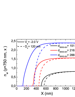
Figure 3: (Color online) Spatial distribution of
the electron density with different heterostructure parameters.
Solid line corresponds to gated samples and dashed line etched
samples. A negative voltage -2.0 V is applied to the gates, whereas
for the etched samples, the depth of etching is fixed to 150 nm. The
distances between electron gas and surface are taken
to be 151 nm, 216 nm, 288 nm. The corresponding depths of the donor
layers are nm, nm and nm, nm, respectively.
Similar calculations are also performed considering
180nm and 266 nm, where
100.8 nm and 151.2 nm, however, the tendencies are left unchanged.
Figure 4: Comparison of densities which are
obtained by analytical formulation, self-consistent calculation
(SCC) and Chklovskii
formalism (CSG).
Figure 5: (a) Schematic representation of the
formation of incompressible strip at . (b) The
variation of the total potential with respect to spatial
coordinates. The solid thick line and shifted thin lines represent
background potential and Landau levels, respectively. Grey region
indicates the enlargement of Landau Levels
due to disorder, by an amount of , whereas the dashed horizontal line is Fermi energy.
Figure 6: Incompressible strip widths of
and considering different Lande- factors. The strip
widths with black lines correspond to the Chklovskii formalism and
red lines correspond to the self-consistent
calculation.
Figure 7: (Color online) The evolution of
incompressible strips also taking account the effect of collision
broadening both considering the gate and the etched defined
samples.