Comparison of different sources for laboratory X-ray microscopy
Abstract
This paper describes the setup of two different solutions for laboratory X-ray microscopy working with geometric magnification. One setup uses thin-film transmission targets with an optimized tungsten-layer thickness and the electron gun and optics of an electron probe micro analyzer to generate a very small X-ray source. The other setup is based on a scanning electron microscope and uses microstructured reflection targets. We also describe the structuring process for these targets.
In both cases we show that resolutions of can be achieved. Also the possibilities of computed tomography for 3D imaging are explored and we show first imaging examples of high-absorption as well as low-absorption specimens to demonstrate the capabilities of the setups.
keywords:
X-ray microscopy, nano-focus X-ray source, laboratory setup1 Introduction
Over the past decades, the spatial resolution in X-ray computed tomography (CT) systems set up at synchrotron beamlines reached in lensless diffraction imaging [1] and using X-ray optics like Fresnel zone-plates [2]. Similar reports from laboratory setups are exceptionally rare. In principle, optics (e.g. zone lenses) can be used in combination with high-power sources to realize specifications comparable to synchrotron beamlines (although with lower photon flux) [3] but this solution comes with several constraints, mainly a. X-ray optics are expensive and very sensitive to vibration, b. such setups are designed for a narrow band of X-ray wavelengths, whereby the available photon energies generally remain below . A possibility to mend these constraints and to perform imaging at higher energies is working in geometric magnification as it is generally the case for typical laboratory micro CT systems. A physical limit for the resolution of such a system is the size of the X-ray source spot, which is around 1 µm. Here, we present two laboratory-based X-ray setups with small source sizes and resolution below and compare their performance to synchrotron imaging and other X-ray microscopy techniques.
2 Experimental Setups
When using the geometric magnification mode (see a schematic in fig. 1a) and a pixelated X-ray detector for microscopy, there are two main resolution constraints: the finite sampling due to the finite pixel size and the projection of the X-ray source spot onto the imaging plane. When working with very high magnification the ultimate resolution limit of the presented systems is the size of the X-ray focal spot. The generation of such small X-ray source sizes can be achieved using a highly focused electron beam hitting a specially designed metal target. The materials chosen in the presented setups are tungsten for its high bremsstrahlung generation due to high atomic number and molybdenum for its characteristic lines that can be sufficiently excited with a electron beam.
2.1 Transmission Setup
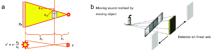
The X-ray microscope set up at the Fraunhofer Development Center X-ray Technology in Fürth is based on the electron gun and optics of an electron probe micro analyzer [4], where the sample chamber has been replaced by a transmission target. The thickness of the X-ray source layer (tungsten) has been optimized for high resolution using Monte Carlo simulations [5]. Due to the low photon flux, a photon counting detector is required. We use the Quad version of the Medipix2 MXR detector with pixels (pitch 55 µm) and a 300 µm silicon sensor layer. Magnifications up to can be achieved. Due to technicalities the use of a rotational axis for 3D imaging is not possible in this setup. So to realize 3D imaging, a laminography setup (see fig. 1b) was chosen. Different views are realized by shifting detector and object on linear axes. This corresponds to a computed tomography setup with limited rotation angle (see also [6]). The laminography angle was at the chosen magnification.
2.2 Reflection Setup
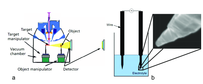
To realize a setup with a rotational axis to have the possibility to perform a full CT scan, a horizontal primary beam offers far more convenience than a system with a vertical primary beam. We modified a JEOL JSM-7100F to serve as an X-ray microscope at Würzburg University. The sample stage has been replaced by a customized stage for both reflection target and object (see fig. 2a). The X-ray detector is placed outside the vacuum chamber and is a Medipix2 MXR with a cadmium telluride sensor layer. The key to the generation of small X-ray source sizes in a reflection target is—in addition to a small electron focus—the reduction of the physical extent of the X-ray generation volume. To achieve this, very sharp metal needles with a tip curvature below are used (see fig. 2b).
3 Results
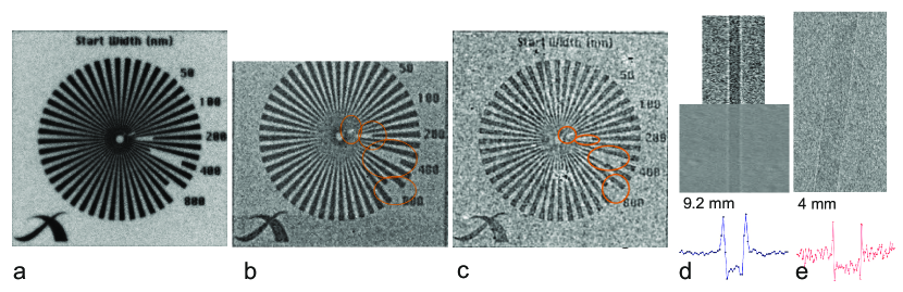
To determine spatial resolution, a star pattern with structures down to 50 nm was imaged with the presented setups and with a commercially available X-ray microscope, the Xradia UltraXRM L200, which is based on Fresnel zone plates (FZP). The resolution achieved with our microscopes is very comparable to the laboratory FZP microscope, however the contrast in our image is lower due to the fact, that we use a tungsten spectrum opposed to monochromatic Cu radiation. The exposure time is longer for the geometric magnification in transmission mode because of the very high source-detector distance. By reducing the source-object distance in reflection mode a higher photon flux on the detector can be realized, thus reducing the exposure time significantly. In all three cases details down to 100 nm are clearly distinguishable (see fig. 3a through c).
To demonstrate the phase contrast capabilities of the systems, low absorbing fibers were used. A 6 µm carbon fiber was imaged in transmission geometry and at a synchrotron beamline under comparable conditions (see fig. 3d). The edge enhancement due to phase contrast is comparable in both images. To test phase contrast imaging in the reflection setup, a 20 µm fiber was used. Even at high magnifications and thus low effective propagations distances edge enhancement is clearly visible.
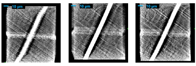
As a first test of the laminographic setup five projections of a small piece of wood marked with two metal wires on top were taken with linear detector/object displacements. A volume reconstruction was performed using an algebraic reconstruction technique. In fig. 4 three different reconstruction layers are shown. High resolution 3D imaging is possible with this setup without applying elaborate numerical treatment to the raw data.
4 Summary and Outlook
Both presented setups for X-ray microscopy based on geometric magnification show a spatial resolution of which is comparable to laboratory X-ray microscopes using synchrotron techniques. Even the very high resolutions achieved at synchrotron beamlines appear to be in reach. We also demonstrated high resolution laminography.
A detailed study of the resolution in 3D imaging is planned to also account for other influences on the quality of the reconstructed volume than the quality of the projection images, e.g. the precision of movement and stability.
Acknowledgements.
The authors gratefully acknowledge the funding of the Bavarian State Ministry of Economic Affairs, Infrastructure, Transport and Technology which supports the project group "Nano-X-ray Systems for Material Characterization" and of the German Research Council (DFG) which, within the framework of its ‘Excellence Initiative‘ supports the Cluster of Excellence ‘Engineering of Advanced Materials‘ at the University of Erlangen-Nuremberg. Special thanks go to Dr. Peter Krüger for providing the resolution test and images from the Xradia microscope.References
- [1] S. P. Krueger et al. Sub-10 nm beam confinement by X-ray waveguides: design, fabrication and characterization of optical properties, J. Synchrotron Rad. 19, 227 (2012)
- [2] W. Chao et al. Soft X-ray microscopy at a spatial resolution better than 15 nm, Nature 435, 1210 (2005)
- [3] A. Tkachuk et al. X-ray computed tomography in Zernike phase contrast mode at 8 keV with 50-nm resolution using Cu rotating anode X-ray source, Z. Kristallogr. 222, 650 (2007)
- [4] R. Hanke et al. Setup of an electron probe micro analyzer for highest resolution radioscopy, Nucl. Instrum. Methods Phys Res., Sect. A 607, 173 (2009)
- [5] F. Nachtrab et al. Laboratory X-ray microscopy with a nano-focus X-ray source, J. Instrum. 6, C11017 (2011)
- [6] J. Zhou et al. Computed laminography for materials testing, Appl. Phys. Lett. 68, 3500 (1996)
- [7] M. Fontio Tip sharpening by normal and reverse electrochemical etching, Rev. Sci. Instrum. 64(1), 159 (1993)