Thin n-in-p pixel sensors and the SLID-ICV vertical integration technology for the ATLAS upgrade at the HL-LHC
Abstract
The R&D activity presented is focused on the development of new modules for the upgrade of the ATLAS pixel system at the High Luminosity LHC (HL-LHC). The performance after irradiation of n-in-p pixel sensors of different active thicknesses is studied, together with an investigation of a novel interconnection technique offered by the Fraunhofer Institute EMFT in Munich, the Solid-Liquid-InterDiffusion (SLID), which is an alternative to the standard solder bump-bonding. The pixel modules are based on thin n-in-p sensors, with an active thickness of 75 m or 150 m, produced at the MPI Semiconductor Laboratory (MPI HLL) and on 100 m thick sensors with active edges, fabricated at VTT, Finland. Hit efficiencies are derived from beam test data for thin devices irradiated up to a fluence of . For the active edge devices, the charge collection properties of the edge pixels before irradiation is discussed in detail, with respect to the inner ones, using measurements with radioactive sources. Beyond the active edge sensors, an additional ingredient needed to design four side buttable modules is the possibility of moving the wire bonding area from the chip surface facing the sensor to the backside, avoiding the implementation of the cantilever extruding beyond the sensor area. The feasibility of this process is under investigation with the FE-I3 SLID modules, where Inter Chip Vias are etched, employing an EMFT technology, with a cross section of 3 m x10 m, at the positions of the original wire bonding pads.
keywords:
Pixel detector , ATLAS , HL-LHC, n-in-p , active edges, vertical integration1 Introduction
Different pixel modules concepts are being developed at the moment in view of the tracker upgrades of the LHC experiments for the Phase II of the High-Luminosity LHC (HL-LHC), in order to cope with the high level of occupancy and radiation damage expected. Detectors with minimal material budget, a larger active area fraction and higher granularity are required, in addition to radiation hardness up to a fluence of , as for example in the case of the inner layer of the ATLAS pixel system. In this context thin planar pixel sensors with reduced inactive edges are good candidates to instruments the new trackers, thanks to their reliability, cost-effectiveness and good charge collection properties at high fluences. An R&D towards the development of thin n-in-p pixel modules of different types, partly including sensors with active edges, is presented. They are designed to achieve, in conjuction with 3D vertical integration technologies, four side buttable modules using Inter Chip Vias (ICV), to move the wire bonding area to the chip backside from the present location on the front side facing the sensor. The n-in-p sensor technology is employed in all the productions described. In addition to an easier fabrication, requiring only a single-sided process in comparison to the double-sided n-in-n sensors, it has also been demonstrated that it achieves the same performance before and after irradiation as the standard n-in-n technology [1, 2, 3]. The homogeneous backside of the n-in-p sensors is also less problematic for the attachment of a handle wafer that is an usual step in the manifacturing of very thin pixel sensors.
2 Thin pixel sensor productions
2.1 MPI HLL thin pixel productions
To investigate the properties of thin sensors and to explore their potential for high energy physics applications two successive pixel productions were carried out at MPI HLL, employing a thinning procedure developed at this facility. This technology makes use of a handle wafer to offer mechanical support during the thinning phase of the active wafer and its subsequent processing The handle wafer can then be removed by using deep anisotropic wet etching with the oxide layer connecting the two wafers acting as etch stopper [4]. The first production contains ATLAS FE-I3 compatible n-in-p sensors with an active thickness of 75 m and it has been interconnected to the read-out chips via the Solid Liquid Interdiffusion technology (SLID) [5], developed by the Fraunhofer Institute EMFT. This pixel production was extensively described in [6, 7, 8] and has been now further tested up to a fluence of , by measurements of charge collection efficiency with a 90Sr radioactive source. These were performed, as all the other charge collection measurements reported in the following, with the ATLAS USBPix system [9] inside a climate chamber keeping the environmental temperature at for not irradiated samples and at for irradiated ones.
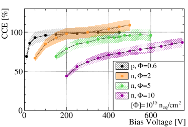
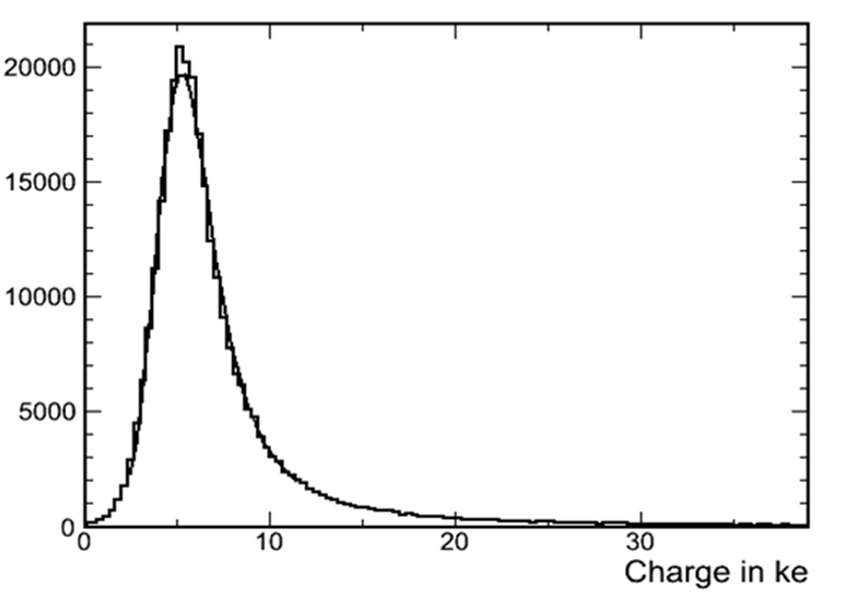
Fig.1(a) shows the charge collection efficiency (CCE), normalized to the charge collected before irradiation, as a function of the bias voltage, for different received fluences. Also at the maximum fluence of , increasing the bias voltage up to 750V, a CCE as high as 90 can be obtained. The Landau distribution of the collected charge at and a bias voltage of 600V is shown in Fig.1(b). The absolute value of the MPV is of the same size as the pre-irradiation one, that lies for the different SLID modules around (4.5-5) ke, in agreement with the expectation for 75 m detectors [10]. Even if the charge collection properties of these very thin sensors deteriorate much less than for thick sensors after irradiation, the signal over threshold ratio for the FE-I3 chip is not high enough to operate them with full hit efficiency, given the minimum treshold range around 2500 e achievable with the present ATLAS read-out chip. The ATLAS FE-I4 chip [11], developed for the IBL project, offers instead the possibility to work at thresholds as low as 1000 e, paving the way to the use thin pixel sensors in the upgraded trackers for Phase II at HL-LHC. The irradiated SLID modules did not present any sign of deterioration of the interconnection, as for example an increase in the number of disconnected channels or of the threshold noise. These findings, even if based on a small statistics of samples, indicate that the SLID interconnection is radiation resistant up to .
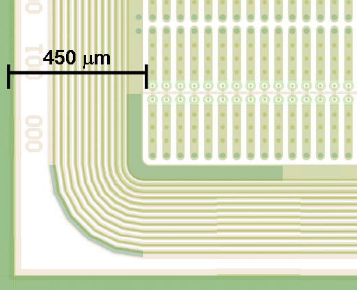
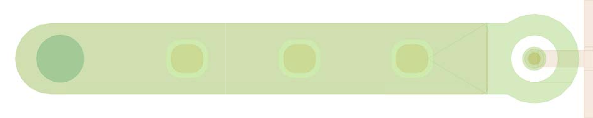
FE-I4 compatible n-in-p sensors, with an active thickness of 150 m were obtained with the second production at MPI HLL (indicated as SOI2 in the following) and they were interconnected with solder bump-bonding at the Fraunhofer Institute IZM, Berlin. The bulk material is the same as for the SLID sensors, FZ p-type, with a resistivity of 2 Kcm. The sensors are characterized by a guard ring scheme containing twelve guard rings resulting in a distance between the last pixel implantation and the sensor edge dedge=450 m (Fig.2).
For the FE-I4A chip no reliable ToT to charge calibration is available [12], so the charge collection properties of the SOI2 assemblies are mainly based on ToT values, in units of the 25 ns bunch crossing clock, which around the tuning point are linearly proportional to the charge.
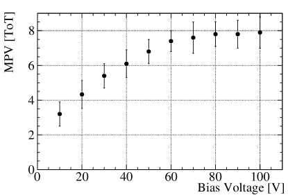
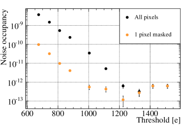
Figure 3 shows the evolution of the most probable value (MPV) of the measured ToT with the measured bias voltage for a not irradiated SOI2 assembly, obtained during scans with a 90Sr source. Given the tuning of 10 ToT for 15 ke, the saturation value of the charge corresponds to (12 2.4) ke, in agreement with the expectation for a 150 m thick sensor [10], where a 20% systematic error has been assigned for the FE-I4A calibration uncertainty. The noise of these FE-I4 assemblies before irradiation is around 120 e, even when operating the chips at thresholds down to 800-1000 e (Fig. 4a). The resulting noise occupancy is very low, as shown as a function of the threshold in Fig. 4b.

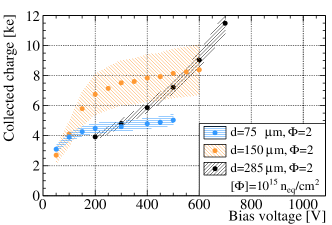
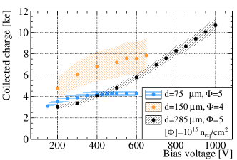
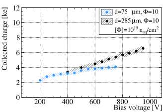
A subsample of the SOI2 modules has undergone an irradiation programm, at a fluence of with 23 MeV protons at the Karlsruhe Institute of Technology (KIT) and at a fluence of with 800 MeV protons at the Los Alamos Neutrons Science Center (LANSCE). The collected charge in scans with a 90Sr source for the SOI2 devices after irradiation is compared in Fig.5 to the values obtained for the 75 m thick sensors and for n-in-p sensors of standard thickness, 285 m, used as reference. These devices were produced at CiS and interconnected to FE-I3 chips via bump-bonding. Details about their characterization before and after irradiations are reported in [1, 3]. The comparison shows that, at least up to a fluence of , where data for SOI2 are available, a higher charge may be obtained with these devices of intermediate thickness. Anyhow with increasing fluence the collected charge for different thicknesses tend to equalize, due to the effect of charge trapping, and at (Fig.5) the 75 m and 285 m shows a very comparable performance up to 600V.
The SOI2 modules were further studied in beam tests with 120 GeV pions at CERN-SPS and 5-6 GeV electrons at DESY, using the EUDET telescope for track reconstruction [13]. A summary of the hit efficiency as a function of the applied bias voltages, up to a fluence of is given in Fig. 6.
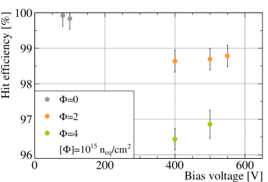
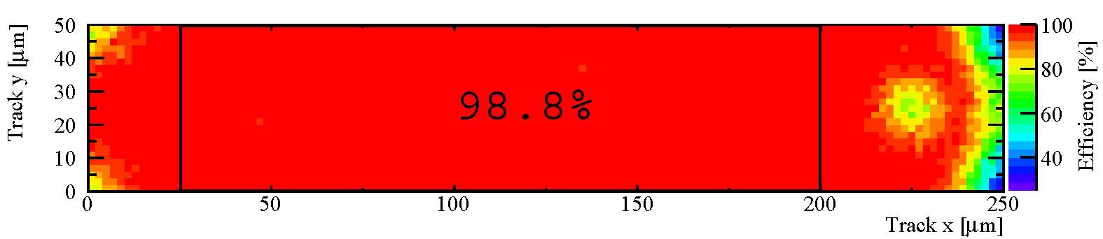
Tracks extrapolated from the telescope are considered as belonging to a specific hit if they are closer than one pixel cell pitch in the long pixel direction and three pixel cell pitches in the short pixel cell direction. These tracks are defined as matched. The hit efficiency is determined as the fraction of matched tracks to a hit in the device and it can be displayed as function of the position in the pixel cell, as predicted by the telescope. Such an efficiency map is shown in Fig.7, together with an image of the pixel cell geometry for the SOI2 modules. The overall efficiencies are (96.50.3) at 400V and (96.90.3) at 500V, where the errors are due to the systematic uncertainty on the track selection. Lower hit efficiencies are found in the corners and in the region corresponding to the bias rail and to the bias dot, when the beam is perpendicular with respect to the devices, as in this case. For inclined tracks part of the efficiency loss in these areas is recovered because the impinging particles traverse also the central region of the pixel cell, where the electric field is higher. The hit efficiencies in central region of the pixel cell, as indicated in Fig.7, are (98.70.3) at 400V and (98.80.3) at 500V

2.2 VTT production of active edge pixel sensors
Active edge n-in-p pixel sensors have been fabricated at VTT within a multi project wafer production [14]. The design of the active area of the FE-I3 and FE-I4 devices and the implementation of the p-spray isolation are derived from the MPI HLL productions. The bulk material of the devices discussed in this paper is p-type FZ, with a resistivity of cm. The sensors were thinned to a thickness of 100 m. The fabrication of thin sensors at VTT exploits, as for the MPI HLL productions, the use of an handle wafer as mechanical support during the grinding phase. The handle wafer is further needed during the etching of the trenches at the sensor borders, a step performed after the electrodes implantation and prior to the final oxidation, implantation activation and Aluminum processing [15]. The trenches are actived with a four-quadrant ion implantation of boron ions, that extends the back-side junction to the vertical edges. The interconnection of the sensors to the FE-I3 and FE-I4 chips has been performed at VTT, with solder bump-bonding. The results shown in the following are relative to three different implementations of the edge regions. The first one, meant to serve as a reference, incorporates eleven guard rings, with the same structure as in the SOI2 production, as well as a bias ring, and it has dedge=460 m. The second design is characterized by only a floating guard ring and a bias ring, connected to the pixel punch-through structures, allowing for the testability before interconnection and the grounding of each individual pixel, even in the case of missing bumps, after interconnection. In this case dedge=125 m (Fig.8(a)). The most aggressive design with active edges, implemented only for FE-I3 sensors, foresees one floating guard ring and dedge=50 m (Fig.8(b)). Since a bias ring structure is not present, also the bias rails and the punch-through structures have been omitted.
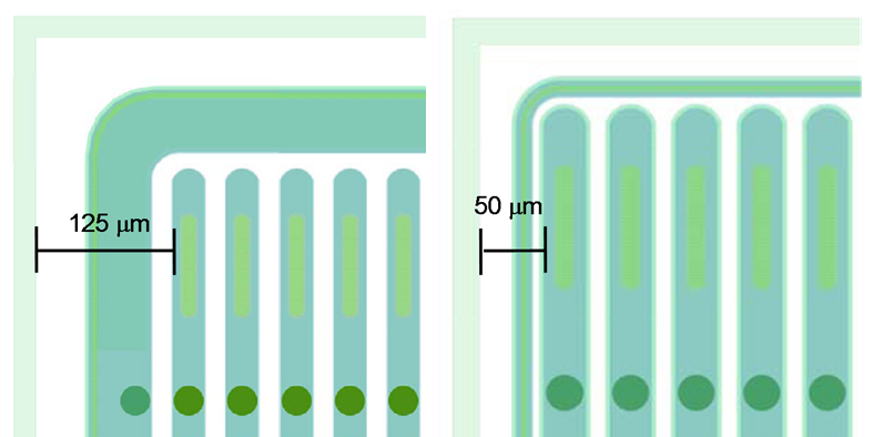
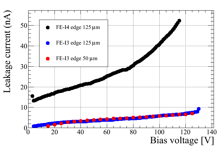
Fig.9 shows the IV curves of not irradiated FE-I3 and FE-I4 modules, with breakdown voltages of the order of (110-120)V and leakage currents well below 10 nA/cm2 over all the voltage range.
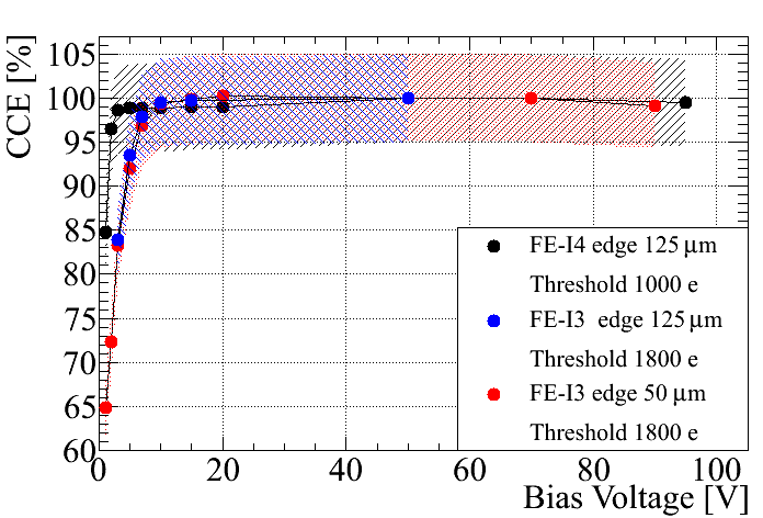
Measurements of charge collection have been performed with these modules after tuning of the FE-I3 samples to a threshold of 1800 e and of the FE-I4 sample to a threshold of 1000 e. Typical values of the threshold noise are measured to be around 190 e for the FE-I3 assemblies and 180 e for the FE-I4 assemblies. The MPV of the collected charge with a 90Sr source, as shown in Fig.10, is normalized to the MPV at 50V, to equilibrate the different absolute scales, due to the offset of the unknown calibration capacitance. A residual systematic uncertainty on the charge ratio is estimated to be 5. The saturation of the charge collection is visible around 10V, in agreement with the value expected from the bulk resistivity, but also at bias voltages as low as 5V, more of 90 of the charge is still collected.
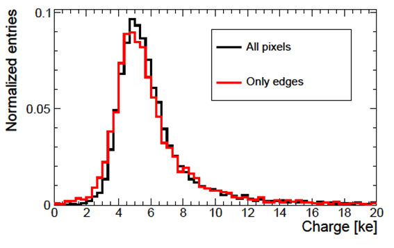
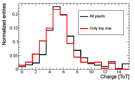
A more detailed analysis of the edge pixel efficiency has been performed, comparing the Landau distributions of these cells to the ones obtained with the full device. The results are shown in Fig.11, where only very small deviations are found between the two sets of curves, both for the FE-I3 devices with dedge=50 m and the FE-I4 devices with dedge=125m. The different binning in the two figures is due to the different ToT resolution for the two generations of chips, 8 bits for the FE-I3 and 4 bits for the FE-I4. The performance of the edge pixels in terms of hit efficiency will be further investigated in the near future with beam tests of these devices.
3 Vertical Integration Technology
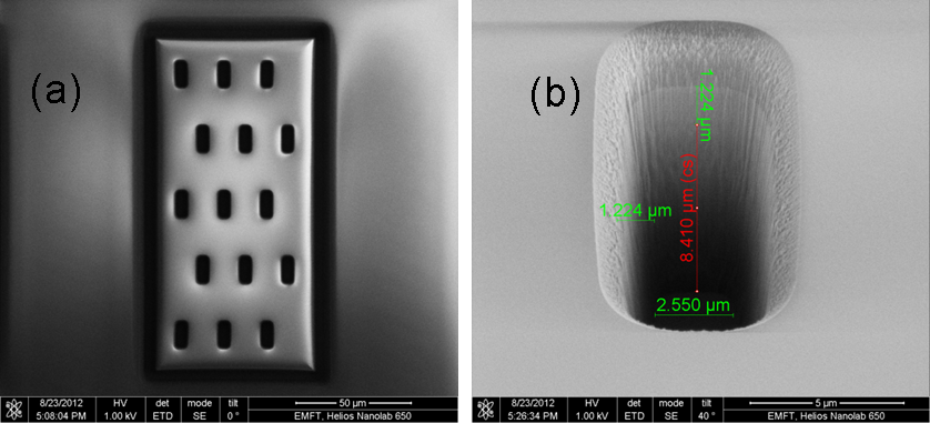
A second step in the R&D activity with the modules interconnected with SLID is the etching of Inter Chip Vias in the FE-I3 chips with the Via Last approach, performed at the Fraunhofer Institute EMFT, to allow for the extraction of signal and services across the chip to the backside. In a 3D compliant design of the pixel electronics, Inter Chip Vias could eventually avoid the need for the cantilever area where the wire bonding pads are presently located. The vias cross-section has been optmized with etching trials in a FE-I3 wafer to be 3x10 m2, and the initial depth to 60 m. After the isolation of the vias with Chemical Vapour Deposition (CVD) of silicon dioxide and the metalization with tungsten filling, the chip wafer front side is passivated and bonded to a handle wafer. The FE-I3 wafer has then to be thinned to 50 m to expose vias and finally new wire bonding pads are applied on the backside, connected to the ICVs with a redistribution layer on the backside. The via preparation has started on the FE-I3 wafer with the etching of the dielectrics below the aluminum layer of the original wire bonding pads (Fig.12).
4 Conclusions
The characterization of pixel modules composed with thin n-in-p sensors, with a thickness range from 75 m to 150 m, interconnected to the ATLAS FE-I3 and FE-I4 read-out chips has been presented. The charge collected after irradiation is compared for different fluences to that obtained with n-in-p pixel assemblies of standard thickness. In the range of fluence from 2 to higher charge may be obtained with the SOI2 devices of 150 m thickness. Anyhow, with increasing fluence, the collected charge for different thicknesses tend to equalize, due to the effect of charge trapping, and at the 75 m and 285 m thick sensors show a very comparable performance up to a bias voltage of 600V. Active edge pixel sensors were fabricated at VTT and they have been studied before irradiation with a 90Sr source to compare the behaviour of the edge and the internal pixels. Negligible differences have been observed in terms of charge collection but further analysis with beam tests are needed to determine the tracking performance of these devices and the effective inactive edge that can be reached with them. Finally, to otbain four side buttable modules, vertical integration technologies are investigated. In particular Inter Chip Vias are being prepared at the moment on FE-I3 chips, to allow for the extraction of signal and services across the chip to the backside. In a 3D compliant chip design Inter Chip Vias could eventually avoid the need for the cantilever area, where the wire bonding pads are presently located, and this would lead, in conjunction with active edge sensors, to pixel modules with no or very reduced inactive edges.
5 Acknowledgements
This work has been partially performed in the framework of the CERN RD50 Collaboration. The authors thank V. Cindro for the irradiation at JSI, A. Dierlamm for the irradiation at KIT and S. Seidel (University of New Mexico) for the irradiations at LANSCE. The irradiations at KIT were supported by the Initiative and Networking Fund of the Helmholtz Association, contract HA-101 (”Physics at the Terascale”). The irradiation at JSI and the beam-tests have received funding from the European Commission under the FP7 Research Infrastructures project AIDA, grant agreement no. 262025.
References
- [1] C. Gallrapp et al., “Performance of novel silicon n-in-p planar pixel sensors”, NIM A, Vol. 679 (2012) 29.
- [2] A. La Rosa et al., “Novel Silicon n-in-p pixel Sensors for the future ATLAS Upgrades”, NIM A, (2012) in press, arXiv:1205.5305
- [3] P. Weigell ”Recent Results of the ATLAS Upgrade Planar Pixel Sensors R&D Project”, these proceedings.
- [4] L. Andricek et al., IEEE Trans. Nucl. Sci., Vol. 51, No. 3. (2004), 1117.
- [5] A. Macchiolo et al., SLID-ICV Vertical Integration Technology for the ATLAS Pixel Upgrades, Physics Procedia, Volume 37, 2012, Pages 1009-1015
- [6] L. Andricek et al, “Development of thin sensors and of a new interconnection technology for the upgrade of the ATLAS pixel system”, Nucl. Instrum. Meth. A 636 (2011) 68.
- [7] A. Macchiolo et al, “Performance of thin pixel sensors irradiated up to a fluence of 1016 neq cm-2 and development of a new interconnection technology for the upgrade of the ATLAS pixel system”, Nucl. Instrum. Meth. A 650 (2011) 145.
- [8] P. Weigell et al., “Characterization of Thin Pixel Sensor Modules Interconnected with SLID Technology Irradiated to a Fluence of 2 ”, JINST, Vol. 6 (2011), C12049
- [9] J. Groe-Knetter et al., USBpix - USB based readout system for ATLAS FE-I3 and FE-I4, 3309 http://icwiki.physik.uni-bonn.de/twiki/bin/view/Systems/UsbPix.
- [10] H. Bichsel, Straggling in thin silicon detectors, Rev. Mod. Phys. 60 (1988) 663.
- [11] M. Garcia-Sciveres et al., “The FE-I4 pixel readout integrated circuit”, 353 NIM A, Vol. 636, No. 1 Supplement (2011), S155
- [12] The ATLAS IBL Collaboration ”Prototype ATLAS IBL Modules using the FE-I4A Front-End Readout Chip”, http://arxiv.org/abs/1209.1906
- [13] J. Weingarten et al.,”Planar Pixel Sensors for the ATLAS Upgrade: Beam Tests results”, accepted by JINST, http://arxiv.org/abs/arXiv:1204.1266
- [14] J. Kalliopuska et al.,”Results of a Multi Project Wafer Process of Edgeless Silicon Pixel Detectors”, these proceedings.
- [15] S. Eränen et al., Nucl. Instrum. Meth. A 607 (2009) 85-88.