Optical Absorption Measurements on Crystalline Silicon Test Masses at 1550 nm
Abstract
Crystalline silicon is currently being discussed as test-mass material for future generations of gravitational wave detectors that will operate at cryogenic temperatures. We present optical absorption measurements on a large-dimension sample of crystalline silicon at a wavelength of 1550 nm at room temperature. The absorption was measured in a high intensity monolithic cavity setup using the photo-thermal self-phase modulation technique. The result for the absorption coefficient of this sample with a specific resistivity of was measured to be for an intensity of 700 W/cm2.
1 Introduction
The initial (1st) and advanced (2nd) generations of interferometric gravitational wave (GW) detectors employ suspended fused silica test masses and use a laser wavelength of 1064 nm [1, 2, 3]. Observatories beyond the 2nd generation will require very high laser powers to reduce the quantum noise at frequencies above , while at lower frequencies it is promising to cool the test masses to cryogenic temperatures to reduce thermal noise.
While at room temperature fused silica shows a high mechanical Q-factor [4] and low optical absorption [5], the mechanical Q-factor decreases by several orders of magnitude at cryogenic temperatures [6, 7]. This makes fused silica unsuitable as test mass material for cryogenically operated GW observatories. Crystalline silicon, however, shows a promising mechanical Q-factor at room temperature that even increases towards cryogenic temperatures up to [8, 9]. Due to the very high absorption coefficient of about 10 /cm at 1064 nm, silicon test-masses require a change to higher laser wavelengths, where the absorption coefficient decreases rapidly [10].
A wavelength of 1550 nm is located within the silicon energy gap and appears promising because of the availability of appropriate optical components and lasers developed for the telecommunication sector. Also, strong squeezed-light sources of are available at 1550 nm [11] to increase the sensitivity of GW detectors beyond the quantum limit [12]. An up to now open question are measurements of the optical absorption coefficient at 1550 nm in the temperature range from a few kelvin up to 300 K. Unfortunately, the measurements presented in [10] were done at slightly shorter wavelength up to 1450 nm. Furthermore, these measurements are a prediction of the absorption coefficient that is based on photo-current measurements. They might not include various effects that lead to optical absorption but do not generate charge carriers. Also the photo-current measurement might not show all absorption effects that are relevant for thermal noise.
In this paper we present direct optical absorption measurements on two silicon samples in large dimensions at room temperature using the photo-thermal self-phase modulation technique [13]. Silicon sample A forms a monolithic cavity. The measurement technique is perfectly adapted to this setup and therefore gives very precise results. While the photo-thermal effect delivers the absorption coefficient, with this method the round-trip loss is measured independently at the same time. Since losses apart from absorption are small for this monolithic setup, the two results confirm each other. Silicon sample B from another manufacturer did not have a dielectric coating and was placed at Brewster’s angle in a Fabry-Perot cavity. Being less stable and containing reflection and scattering losses, the measurement with this setup only served as an order of magnitude estimation to yield an approximate upper and lower limits of the absorption. The slightly different setup backed the fact that the optical absorption found for sample A was not coincidentally untypically high or low and was not mainly caused by the dielectric coatings.
2 Absorption Measurements on Silicon Sample A
Sample A was manufactured by Siltronic AG [14] with the Czochralski technique. The crystal’s orientation is (111). The material has a specific resistivity of about 11 kcm, which indicates a low doping or contamination with foreign atoms. According to the manufacturer it is a low boron doping, which is a p-donator. This means the impurity concentration is approximately atoms per cm3 [15]. Sample A is the purest material available to us in the required dimensions at ordering time.
The substrate was cut and polished into a cylinder with the rotation axis being parallel to the (111) axis. The cylinder’s diameter was ( is the substrate radius), the length was . The end surfaces were polished to be convex curved with a radius of curvature of 1 m to form a cavity with a free spectral range (FSR) of 663 MHz.
The substrate’s curved end surfaces were coated using ion beam sputtering (IBS). The high-reflection coatings consisted of SiO2 and Ta2O5 and had a design reflectivity of 99.9 at a wavelength of 1550 nm. Hence, the coated substrate formed a monolithic cavity with beam propagation along the (111) axis.
2.1 Experimental Setup
Fig. 1 shows a schematic of the experimental setup. A laser beam at a wavelength of 1550 nm was mode-matched to the eigenmode of the monolithic cavity. To calibrate the time-axis of our measurements we used frequency markers. An electro optical modulator (EOM) generated these frequency markers by imprinting sidebands at a frequency of 43.57 MHz onto the light field.
Photo detector PD1 detected the reflected light, which was separated from the incident field by a combination of a Faraday rotator and a polarizing beam splitter (PBS). Demodulating PD1 and creating a Pound-Drever-Hall-type [16] error-signal generated the frequency markers.
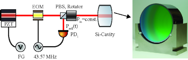
For exploiting the photo-thermal self-phase modulation technique, the laser frequency was scanned around the resonance frequency of the cavity via a piezo electric transducer (PZT). An increasing wavelength corresponded to a shortening of the cavity and a decreasing wavelength to a lengthening of the cavity.
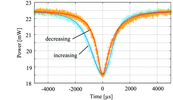
The input laser power was 22 mW for all measurements resulting in an intensity of within the substrate. We performed several measurements by varying the scan frequency starting from 0.2 Hz to 49 Hz in 18 steps with a constant scan amplitude. The frequency for each measurement number can be found in Tab. 1. Because the PZT showed a hysteresis, the actual wavelength change had to be calibrated for each frequency for increasing and decreasing wavelength. The time axis of each measurement was calibrated from the scan frequency, the FSR, and the detected error signal. In Figure 2, an example measurement for a scan frequency of 0.6 Hz is shown. This frequency corresponds to a scan velocity of about 2 ms/peak at full width half maximum (FWHM). The yellow crosses (narrow peak) show the measured peak for a decreasing wavelength with the corresponding simulation in red (solid line). The light blue crosses (broad peak) show the peak for an increasing wavelength with the simulation in dark blue (solid line). Without absorption, the two peaks were identical.
| Measurement number | 1 | 2 | 3 | 4 | 5 | 6 | 7 | 8 | 9 |
|---|---|---|---|---|---|---|---|---|---|
| Scan frequency [Hz] | 0.2 | 0.4 | 0.6 | 0.8 | 1.0 | 1.2 | 1.4 | 1.6 | 1.8 |
| Measurement number | 10 | 11 | 12 | 13 | 14 | 15 | 16 | 17 | 18 |
| Scan frequency [Hz] | 2 | 4 | 6 | 8 | 10 | 20 | 30 | 40 | 49 |
2.2 Measurement Analysis and Results
To calculate the absorption coefficient from the measured peaks as shown in Fig. 2, the peaks were fitted. For the fitting process we used the parameters from Table 2 as well as the in-coupling reflectivity R1, the effective out-coupling reflectivity , and for measurements with a visible thermal effect as fitting parameters. Here, is the effective reflection of the out-coupling coating accounting for the entire cavity round trip loss apart from the transmission of the in-coupling coating. The values for material parameters were taken from literature [17, 18, 19]. For the geometric parameters, we used values based on our best knowledge of the cavity design. A Nelder-Mead algorithm was run to find the best set of fitting parameters minimizing the standard deviation of measurement and simulation. 13 of 18 single measurements showed a visible thermal effect and were used to derive the absorption. The remaining five measurements showed no thermal effect due to the high scan-frequency. 8 Hz was the threshold above which no thermal effect occurred. All 18 measurements were used to derive R1 and . The results obtained from measurements without thermal effect were consistent with the remaining results.
Figure 3(a) shows the results for the absorption coefficient derived from the 13 different measurements (dark-green dots). The purple lines show the mean value of all single results and their standard deviation which is ().
| Geometric parameters | Source | |
| crystal radius | specified by manufacturer | |
| crystal length | specified by manufacturer | |
| beam waist | 217.8 m | calculated from , and |
| Material parameters | ||
| index of refraction | [17] | |
| thermal expansion | [18] | |
| thermal refr. coeff. dd | [19] | |
| specific heat | [18] | |
| density | [18] | |
| thermal conductivity | [18] |
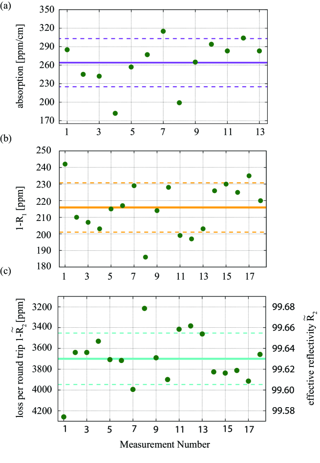
The results for the (power) reflection R1 of the in-coupling coating are shown in Figure 3(b). The mean value and standard deviation of all 18 single measurements is . Measurement numbers 14–18 did, as stated above, not exhibit a visible thermal effect.
Figure 3(c) shows the results for for all single measurements (dark-green dots) and their mean value and standard deviation (turquoise lines) of . This result was used to cross-check the obtained absorption values. An absorption of per round-trip results in an effective absorption coefficient of taking into consideration the round-trip length of 13 cm. The round-trip loss added to results in a new effective reflection that still contains the cavity scattering loss. Since the pure reflection can be assumed to be very similar to (identical coating design, but different coating runs) the results for the three parameters agree perfectly. This is an additional consistency check and not an automatical consequence of the simulation.
We repeated the series of measurements for a polarization rotated by 90∘. Further we exchanged in-coupling and out-coupling coating and repeated the measurements for the two polarizations. As expected, in each case the results for the absorption coefficient agreed with the result presented above within the error bars.
2.3 Error Propagation
The error bar of 39 ppm or corresponds to the standard deviation of 13 independent measurements using different scan-velocities. An additional error bar arises from uncertainties in the simulation input parameters. To estimate this error, we individually changed the input parameters listed in Table 2 by and recalculated R1, and . We found that for most parameters the influence on is approximately linear and none of the changed parameters caused a change of the result for by more than .
For , the error bar of the value from literature is in the order of [17] and therefore negligible, the uncertainty of is in the same order of magnitude [19]. and affect the result as a sum. Since , an uncertainty of is negligible. The error bars of , and are not known to us. We estimate that the uncertainties of the cavity geometric input parameters as well as for the calibration of the time axis and in the measurement of the mode-matching are below 10 %.
If the simulation input parameters are precise within , our statistical error bar of is the dominating error contribution.
3 Measurements on Silicon Sample B
The absorption measured with sample A was unexpectedly high (see discussion). To verify that this sample did not absorb untypically much, or that the coating did not cause the absorption, a second experiment with a different sample B was performed. The two samples differed in manufacturer and crystal orientation.
A cylindric substrate with one inch diameter and 3.5 cm length was manufactured by Mateck [20] in (100) orientation using the Czochralski procedure. The (100) axis is the rotation axis of the cylinder. The cylinder end surfaces were polished to be parallel with a tolerance of . The material was declared by the manufacturer to be undoped with a resistivity of .
The substrate was placed in a resonator at Brewster’s angle of 74 ∘ to minimize round trip loss due to reflection at the substrate surface (see Figure 4). The mirrors were clamped to an aluminium spacer. The laser beam coupled into the cavity through the in-coupling mirror M1. The reflected beam power Prefl was detected in reflection of the beam splitter (BS). (Using the BS instead of the Faraday rotator and PBS combination in the first setup, does not change anything for the experiment.) The modulation of the laser, the calibration of the time axis and the measurement procedure were identical to the procedures described in Section 2.1 for the monolithic cavity setup.
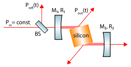
Entering the substrate at Brewster’s angle causes an elliptical beam profile within the substrate. Since not necessary for other experiments, a non-circular beam profile is not implemented in our simulation program. The discussed measurement had the goal of independently determining a lower limit for the optical absorption to confront the obtained value with the results from sample A. Therefore, a calculation of an upper limit for the power density and thus for the heat distribution within the substrate is sufficient. This is given by a circular beam profile with the radius of the minor semi-axis of the elliptical profile. Since a higher power density requires a smaller absorption to cause the same thermal effect, this assumption yields a lower limit for the absorption coefficient.
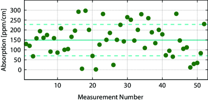
From 52 single measurements, the lower limit for the absorption was found to be . The results of the single measurements are shown in Figure 5 (green dots). The mean value of all measurements with the standard deviation are depicted by the light-blue line and the light-blue dashed lines, respectively. Despite a shared spacer for mirrors and substrate, the external cavity setup proved to be instable and prone to acoustical disturbances, which caused large error bars due to the statistical fluctuations of the detected peaks.
The error propagation was already discussed for sample A. The uncertainty of the result is dominated by the large standard deviation, while the errors in the material parameters are negligible in first order approximation.
Apart from the elliptical beam profile, the large statistical error shows that the second setup is much more instable and therefore disadvantageous compared to the monolithic setup. Nevertheless, the lower limit for the absorption of allows the conclusion that the absorption in sample A did not primarily originate in the dielectric coatings.
In a second series of measurements, the round trip loss of the cavity was measured. This provided an the upper limit for the absorption coefficient. For this measurement, two mirrors with identical coatings were used and the round-trip loss was minimized by inclining and rotating the substrate. The maximum impedance matching was found to be . (An impedance matching of means that the reflected power at resonance is zero.) Using the design reflectivity of R1=R the optical loss was calculated to L. LRT contains the entire optical loss that consists of absorption of and scattering at the mirror coatings as well as of the reflection and scattering at the silicon substrate surface. The latter occurs twice per round trip because of entering and leaving the substrate, respectively. These reflections are caused by non-perfect plan-parallel end surfaces of the substrate, the wave-front distortion of the beam, scattering and limitations in fine-adjustment. The laser beam passes of the substrate per round trip. This results in a loss of and forms the upper limit for the absorption coefficient.
Nevertheless, the result of for silicon sample B suggests that the result obtained with sample A was typical for samples of the degree of purity involved.
4 Discussion
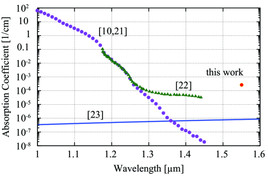
Fig. 6 shows the absorption result from the present work in comparison to earlier absorption results from spectral response measurements on solar cells taken from literature (purple dots and green triangles) [21, 22] and to a theoretical prediction of the absorption caused by the residual boron contamination of sample A [24].
Previous measurements [21, 22] found a much lower absorption of silicon than measured here. However, these results are also not consistent. Although no measurements at 1550 nm are available, the absorption measurements from Keevers and Green predict an absorption coefficient of at 1550 nm [10], while the measurements from Anagnostopoulos predict an absorption coefficient in the order of [22]. Green and Keevers explain their much lower absorption results by suggesting contamination of Anagnostopoulos’ sample, due to doping or unintended foreign atoms. The assumed kind of contamination is, however, not specified in either of the two publications. The band-band absorption is the lower absorption limit for intrinsic crystalline silicon. Preliminary results obtained by Degallaix et al. [23] point to a light-intensity dependent absorption in silicon. An estimation based on the power density in our setup showed that our result is not significantly influenced by that effect.
Even very low doping or contamination of the silicon samples can dominate the band-band absorption in the infrared region due to the free carrier absorption [24]. Since the semiconductor industry is by far the largest area of application for crystalline silicon, samples almost always are doped or at least slightly contaminated with the doping material that is normally used in the apparatus for the crystal growth. A specific resistivity of , which is the specific resistivity of sample A, corresponds to a p-doping of (N is the number of doping atoms). The number of doping atoms was calculated from the specific resistivity using [15]. The blue line in fig. 6 shows for a p-doping of (blue line) calculated using [24]. and the number of doping atoms are proportional [25]. This theory predicts an absorption coefficient of for sample A, which is two orders of magnitude below our measurement results. Therefore, this doping theory does not explain the absorption of samples A and B. However, the theories for absorption due to doping generally are optimized for much higher doping than in our case. It is therefore possible that the prediction for residual-doping-induced absorption is not accurate, and further theoretical and experimental investigations are required to clarify this issue. Another possible and plausible explanation for the deviation from the numbers published by Keevers and Green is that their photo-current measurements did not include effects that, while leading to optical absorption, would not lead to generation of carrier charges. Such photo-current measurements are thus not unconditionally transferable to optical absorption and may rather be used to derive a lower limit. Finally, the specific resistivity values provided by the manufacturers not necessarily provide information about all kinds of contamination present in the crystal and thus can not be used as an absolute measure for the crystal’s purity. Further investigation of the residual contamination is required to derive a model for the dependence of the optical absorption on residual doping and contaminations, which are not reflected in the specific resistivity value.
5 Conclusion
We measured the room temperature absorption coefficient of two silicon samples A and B which differed in manufacturer and crystal orientation. According to the manufacturer, sample A had a residual contamination by boron atoms with . For sample B, the specific resistivity was specified to be , this corresponds to a p-doping of .
For sample A, a result of was obtained. The consistent results for optical absorption and round trip loss induce that no other process apart from the optical absorption provides a significant loss contribution.
For sample B, upper and lower limits of were derived for the absorption coefficient. This confirmed the result for sample A not to be extraordinarily high or low. Since uncoated, the measurement of sample B additionally proved that the absorption of sample A did not originate in the dielectric coatings but was due to absorption in the bulk substrate and/or the surface oxide layers. An identification of the origin of the optical test mass absorption will be subject to further measurements that shall be conducted in the near future.
Acknowledgements
We acknowledge support from the SFB/Transregio 7, the International Max Planck Research School (IMPRS) on Gravitational Wave Astronomy, and from QUEST, the centre for Quantum Engineering and Space-Time Research.
References
References
- [1] Harry G M (for the LIGO Scientific Collaboration) 2010 Advanced LIGO: the next generation of gravitational wave detectors Class. Quantum Grav 27, 084006
- [2] Lück H, Affeldt C, Degallaix J, Freise A, Grote H, Hewitson M, Hild S, Leong J, Prijatelj M, Strain K A, Willke B, Wittel H and Danzmann K 2010 The upgrade of GEO 600 J. Phys.: Conf. Ser. 228 012012
- [3] 2010 Accadia T et al. Status and perspectives of the Virgo gravitational wave detector J. Phys.: Conf. Ser. 203 012074
- [4] Penn S D, Ageev A, Busby D, Harry G M, Gretarsson A M, Numata K and Willems P 2006 Frequency and surface dependence of the mechanical loss in fused silica Physics Letters A 352 3–6
- [5] Hild S, Lück H, Winkler W, Strain K, Grote H, Smith J, Malec M, Hewitson M, Willke B, Hough J and Danzmann K 2006 Measurement of a low-absorption sample of OH-reduced fused silica Applied Optics 45 7269–7272
- [6] Schwarz C et al. 2009 Proceedings of ICEC22-ICMC2008 edited by Chang H-M et al. 978-89-957138-2-2
- [7] Schnabel R, Britzger M, Brückner F, Burmeister O, Danzmann K, Dück J, Eberle T, Friedrich D, Lück H, Mehmet M, Nawrodt R, Steinlechner S and Willke B 2010 Building blocks for future detectors: Silicon test masses and 1550 nm laser light Journal of Physics Conference Series 228 012029
- [8] Nawrodt R, Zimmer A, Koettig T, Schwarz C, Heinert D, Hudl M, Neubert R, Thürk M, Tünnermann A, Nietzsche S, Vodel W and Seidel P 2008 High mechanical Q-factor measurements on silicon bulk samples Journal of Physics: Conference Series 122 012008
- [9] McGuigan D F, Lam C C, Gram R Q, Hoffman A W and Douglass D H 1978 Measurements of the Mechanical Q of Single-Crystal Silicon at Low Temperatures Journal of Low Temperature Physics 30 621–629
- [10] Keevers M J and Green M A 1995 Absorption edge of silicon from solar cell spectral response measurements Appl. Phys. Lett. 66 174–176
- [11] Mehmet M, Ast S, Eberle T, Steinlechner S, Vahlbruch H and Schnabel R 2011 Squeezed light at 1550 nm with a quantum noise reduction of 12.3 dB Optics Express 19, 25763–25772
- [12] The LIGO Scientific Collaboration 2011 A gravitational wave observatory operating beyond the quantum shot-noise limit Nature Physics 7, 962–965
- [13] Lastzka N, Steinlechner J, Steinlechner S and Schnabel R 2010 Measuring small absorptions by exploiting photothermal self-phase modulation Applied Optics 49 5391–5398
- [14] www.siltronic.com
- [15] Sze S M and Irvin J C 1968 Resistivity, Mobility and Impurity Levels in GaAs, Ge, and Si at 300∘K Solid-State Electronics Pergamon Press 11 599–602
- [16] Black E 2001 An introduction to Pound-Drever-Hall laser frequency stabilization American Journal of Physics 69 79–87
- [17] Frey B J, Leviton D B and Madison T J 2006 Temperature dependent refractive index of silicon and germanium arXiv:physics/0606168v1
- [18] Weber M J 2003 Handbook of optical materials CRC Press LLC Boca Raton (FL) USA
- [19] Komma J, Schwarz C, Hofmann G, Heinert D and Nawrodt R 2012 Thermo-optic coefficient of silicon at 1550nm and cryogenic temperatures APPLIED PHYSICS LETTERS 101 041905
- [20] MaTecK GmbH Jülich www.mateck.de
- [21] Green M A and Keevers M J 1995 Optical Properties of Intrinsic Silicon at 300K Progress in Photovoltaics:Research and Applications 3 189–192
- [22] Anagnostopoulos C and Sadasiv G 1973 Fine Structure in the Optical-Absorption Edge of Silicon Phys. Rev. B 7 733–739
- [23] Degallaix J, Forest D, Carcy C, Pinard L and Flaminio R 2012 Presentation at the 4th Einstein Telescope Symposium: December 4th 2012, Hannover, Germany, https://tds.ego-gw.it/itf/tds/file.php?callFile=ET-0024A-12.pdf
- [24] Soref R A and Lorenzo J P 1986 All-Silicon Active and Passive Guided-Wave Components for =1.3 and Journal of Quantum Electronics QE-22 873–879
- [25] Schmid P E 1981 Optical absorption in heavily doped silicon Phys. Rev. B 23 5531–5536