Impact of graphene quantum capacitance on transport spectroscopy
Abstract
We demonstrate experimentally that graphene quantum capacitance can have a strong impact on transport spectroscopy through the interplay with nearby charge reservoirs. The effect is elucidated in a field-effect-gated epitaxial graphene device, in which interface states serve as charge reservoirs. The Fermi-level dependence of is manifested as an unusual parabolic gate voltage () dependence of the carrier density, centered on the Dirac point. Consequently, in high magnetic fields , the spectroscopy of longitudinal resistance () vs. represents the structure of the unequally spaced relativistic graphene Landau levels (LLs). mapping vs. and thus reveals the vital role of the zero-energy LL on the development of the anomalously wide quantum Hall state.
pacs:
72.80.Vp, 73.43.-f, 74.25.F-, 73.22.PrI Introduction
Graphene has been attracting great interest, much of which is linked to the behavior of its charge carriers that mimic massless Dirac fermions as a result of the relativistic band structure referred to as Dirac cones. Novoselov ; Novoselov2 ; Zhang Among various experimental techniques designed to probe Dirac cones, the measurement of quantum capacitance , Chen ; XiaNatureNanotech ; Ponomarenko ; Ensslin ; XiaAPL defined as with the charge carrier density and the Fermi level (: elementary charge), is unique in that it directly probes the density of states (DOS) at the Fermi level. The effects of usually appear as a minor modification to the measured capacitance, expressed as (: capacitance of gate oxide), which thus becomes discernible only in the vicinity of the charge neutrality point (Dirac point) where . Chen ; XiaNatureNanotech ; Ponomarenko ; Ensslin ; XiaAPL Using a very thin ( nm) high dielectric gate insulator, Ponomarenko et al. were able to measure graphene quantum capacitance with high accuracy, which revealed the smearing of the Dirac cone by charge puddles and the broadening of relativistic graphene Landau levels (LLs) in high magnetic fields (). Ponomarenko These studies demonstrate that indeed depends on Chen ; XiaNatureNanotech ; Ponomarenko ; Ensslin ; XiaAPL unlike in conventional two-dimensional (2D) systems. Luryi However, with the standard setup for transport spectroscopy using a gate oxide a few nm thick, the feature of graphene quantum capacitance reflecting the Dirac cone is not manifested, because it is overridden by ; accordingly, the usual linear relation between and gate voltage is routinely assumed as in conventional 2D systems.
In this paper, we demonstrate that graphene quantum capacitance can have an impact on transport spectroscopy over a wide carrier density range away from the Dirac point, through the interplay with nearby charge reservoirs. Here we elucidate the effect in high-mobility field-effect-gated epitaxial graphene, in which the role of charge reservoirs is played by interface states that exist at the SiC substrate and in the gate insulator. The interplay between the -dependent graphene quantum capacitance and the nearly energy-independent interface state DOS modifies the usual relation (: gate voltage at the Dirac point) into a nontrivial one [i.e., ()2] when the interface states dominate. In high , transport spectroscopy vs. consequently emerges as a manifestation of the energy spectrum of the unequally spaced relativistic graphene LLs. This additionally allows us to deduce the energy width of the extended state in the LL (: the LL orbital index) from the width of the longitudinal resistance () peak. The mapping of vs. and provides an intuitive picture of the vital role of the zero-energy LL in the development of the anomalously wide quantum Hall (QH) state, which has been commonly observed in low-density epitaxial graphene. Jobst ; Janssen ; Lara-Avila ; Wu ; ShenJAP ; Jouault We explain our data coherently by using a device model containing interface states. Our results suggest that similar effects, although not as apparent, may be at work in the transport spectroscopy of graphene including nano- and heterostructures.Tutuc
II Sample and method
Our epitaxial graphene device was fabricated from graphene grown on 4H-SiC(0001) and has a top gate with a gate insulator made of HSQ/SiO2 (120 nm/40 nm). TanabeAPEX The device is a Hall-bar with width = 5 m and length = 15 m. For comparison, we also studied an exfoliated graphene device of a comparable size, fabricated on a Si/SiO2 (285 nm) substrate using the conventional method. Novoselov Transport measurements were performed at a temperature of 1.5 K using a standard lock-in technique with a current of less than 1 A. For epitaxial graphene, we have studied more than ten devices fabricated from several different SiC/graphene wafers. Here we present data taken from one sample for the consistency of the analysis, but we emphasize that similar results are obtained for all the samples studied.
III EXPERIMENT AND ANALYSIS
III.1 Results in zero and low magnetic fields
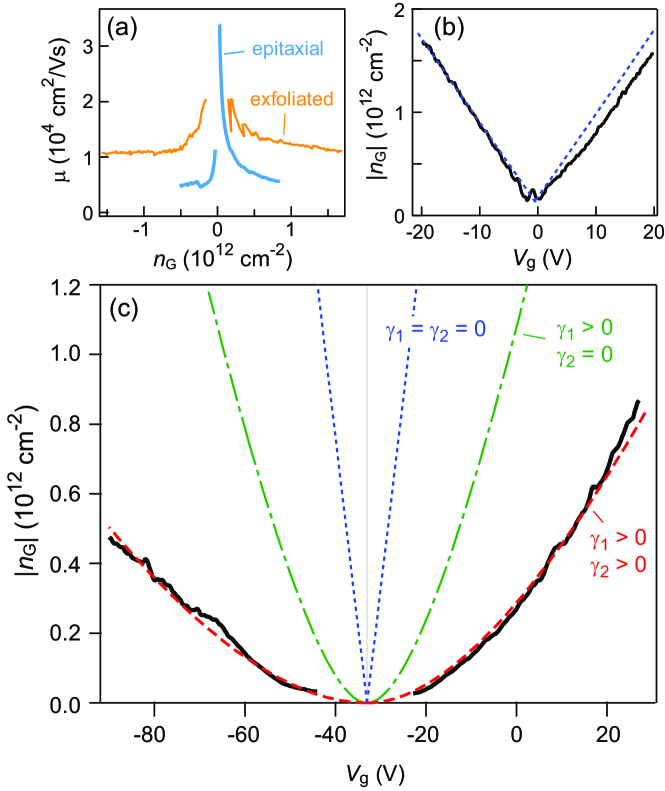
Figure 1(a) compares the mobility [] of exfoliated and epitaxial graphene devices, plotted as a function of determined from the Hall coefficient in low fields ( 0.5 T). The two devices have comparably high mobilities, whereas a striking difference is observed for the dependence of . Exfoliated graphene shows a normal relation with a slope that is in accordance with the gate capacitance [Fig. 1(b)]. In contrast, the change in with in epitaxial graphene is much smaller than that expected from the gate capacitance, [dotted line in Fig. 1(c)]. More intriguingly, the dependence of on is nonlinear, being parabolic-like around the Dirac point. The symmetry of the feature around the Dirac point implies that it arises from an intrinsic property of graphene.
The reduced action of on indicates the existence of carrier trap states that accommodate a portion of the charges induced by the gate. The observed parabolic dependence , combined with specific to monolayer graphene, Novoselov2 suggests that in the present case the unusual relation holds, as opposed to the normal behavior . As we show below, this can be explained if the trap states have a large and nearly constant DOS.
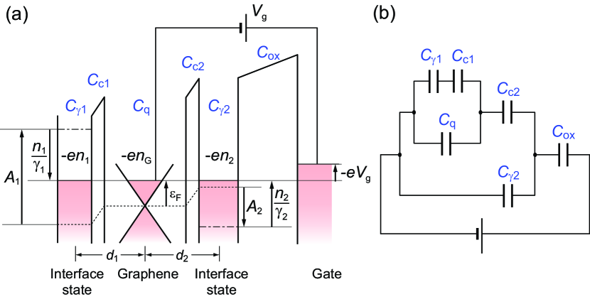
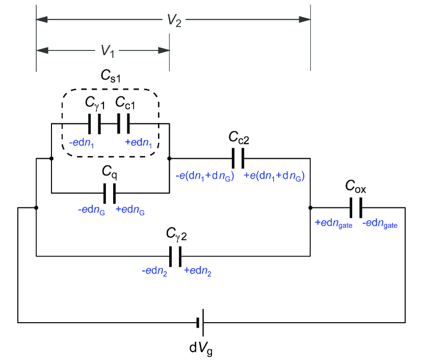
We developed a model containing interface states below and above the graphene layer, each of which has a constant DOS and geometrical capacitance with graphene, where and are the distance and effective permittivity between graphene and the interface states below (above) [Fig. 2(a)]. The lower interface states represent the dangling-bond states at the SiC substrate, Janssen ; Kopilov ; Varchon ; Sonde while the upper interface states represent charge traps in the gate insulator. Sze By noting that the -induced charge redistribution between graphene and the interface states is influenced by both the electrostatic potentials associated with and the chemical potentials associated with their quantum capacitances given by Chen ; XiaNatureNanotech ; Ponomarenko ; Ensslin ; XiaAPL and , Luryi we can describe the charge redistribution as follows:
| (1) |
Here, is the series capacitance of and . The corresponding equivalent circuit is shown in Fig. 2(b). SM While Eq. (1) is a relation that generally holds for 2D systems, in graphene it has a non-trivial consequence because is not proportional to . That is, in the equivalent circuit is a function of , which leads to a nonlinear relation between and .
We calculated vs. by solving Eq. (1) with ( m/s Ponomarenko ), nm, and (: vacuum permittivity). calcFootnote1 As shown by the dashed line in Fig. 1(c), the data can be fitted well with physically reasonable values, e.g., and eV-1cm-2 for (). footnoteSign Here, we used the same value as in Refs. Janssen, and Kopilov, . We emphasize that the model in Ref. Kopilov, , which assumes only interface states below graphene, cannot account for our results. A calculation with and yields a dependence much larger than that observed [dash-dotted line in Fig. 1(c)]. footnoteA
Equation (1) demonstrates that the linear relation between and , which usually does not hold for transport spectroscopy of graphene, does appear when the second term on the left-hand side dominates the first term. For the and values deduced above, we find this condition to be met when cm-2. Consequently, measurements in high provide the spectroscopy of the unique LL structure characteristic of Dirac electrons in graphene, as demonstrated below.
III.2 Results in high magnetic fields
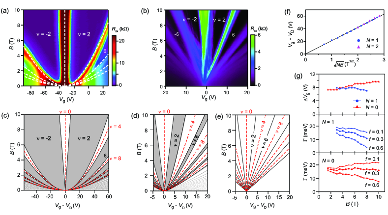
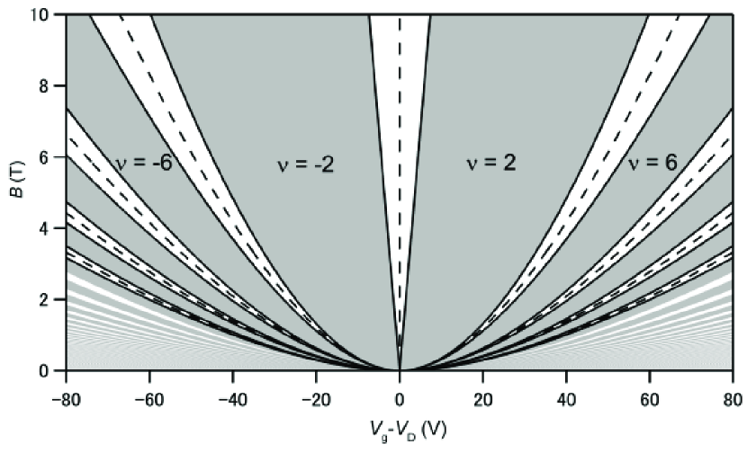
Figure 3(a) shows a color-scale plot of measured as a function of and . peaks at separating adjacent QH regions appear as sets of unequally spaced parabolic curves centered on the Dirac point and emanating from . [For comparison, we show the data for exfoliated graphene in Fig. 3(b).] The white dashed lines in Fig. 3(a) represent the positions at which the four-fold degenerate graphene LLs become half filled, i.e., (), calculated from and deduced from the low-field data in Fig. 1(c). As the agreement between the experiment and the calculation shows, our model remains valid in high fields and captures the essence of the gate- and field-induced charge redistribution. In Fig. 3(f), the positions of the peaks in , measured from , are plotted for the and LLs with the abscissa scaled to . The observed relation confirms that the mapping of peaks vs. and represents the structure of relativistic graphene LLs.
As we show below, a more profound consequence of the relation is that, when the Fermi level is located at one of the LLs, serves as a measure of the energy position of that LL not only at its center but also at its tail. By substituting in Eq. (1) with the energy of the graphene LL, , where is the orbital index of the highest occupied level, we are able to calculate and hence (: Planck’s constant) as a function of and without unknown parameters. Figure 3(c) depicts the result calculated using and appropriate to our sample. In the diagram, regions with integer (non-integer) fillings are shown in gray (white) and the positions of half fillings () by dashed lines. The - plane is filled mostly with integer- regions, and non-integer appears only in narrow regions around half fillings. This happens because the Fermi level can lie in the gap between LLs by virtue of the interface states, whose DOS exists in the LL gap. The impact of the interface states is made clearer by comparing Fig. 3(c) with the calculations performed with smaller [Figs. 3(d) and 3(e)]. As increases, the LL fan diagram becomes more nonlinear and, at the same time, integer regions become increasingly dominant over non-integer regions.
Our model accounts for the main feature of the experimental results sufficiently well. Yet, it is noticeable that at low the measured peaks are broader than the calculated widths of the non-integer regions. This is because the model does not take into account the LL broadening caused by disorder. This, in turn, allows us to extract the energy width of the extended states from the widths of the peaks. Note that is otherwise not accessible through other conventional techniques including capacitance, Ponomarenko infrared, infrared and scanning tunneling Andrei spectroscopy, which do not distinguish extended and localized states. footnoteTutuc When the overlap with adjacent LLs is negligible, the full width at half maximum (FWHM) of an peak is shown to be related to as
| (2) |
Here, is the fraction of the extended state with respect to the whole LL DOS and is the fraction of the LL DOS within its FWHM ( for Gaussian and for Lorentzian). SM In Fig. 3(g), we plot the measured and deduced for the and LLs assuming different values as a function of . GaussOrLorentz Our analysis yields meV for the LL with reasonable accuracy at low , even without any knowledge of the exact or values. Although for the LL is contingent on the stronger overlap with the LL, we can say that ’s for the LL and LL at low are of similar magnitude. This allows for an interesting contrast to be made with our results and the activation gap measurements reported for exfoliated graphene, the latter suggesting that the LL is much sharper than higher LLs. Giesbers We may also make a nice comparison with theory predicting that the and other LLs exhibit different behavior for certain types of disorder. Nomura ; Katsnelson ; Kawarabayashi
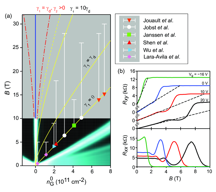
As shown in Fig. 4(b), the QH effect persists up to unexpectedly high fields, a feature commonly observed in epitaxial graphene with low carrier densities. Jobst ; Janssen ; Lara-Avila ; Wu ; ShenJAP ; Jouault The effect has recently been discussed by Janssen et al. in terms of -induced charge transfer from the dangling-bond states to graphene. Janssen As we have demonstrated in Figs. 3(a) and 3(c), when the interface state DOS is high, mapping vs. and mimics the graphene LL structure. This intuitively shows that the anomalously wide QH region is a consequence of the special property of the LL, namely, that it has zero energy independent of . With our model, the critical field at which the Fermi level enters the LL is given by
| (3) |
as a function of the zero-field carrier density . SM The second term represents the effect of -induced charge transfer. Equation (3) reveals that interface states both above and below the graphene layer contribute to the -induced charge transfer, which increases irrespective of whether they are donors or acceptors. Equation (3) also allows us to analyze all reported data on the anomalously wide QH state, including ours, in a single framework by plotting them vs. .
Figure 4(a) summarizes the range over which the plateau was extended toward high in previous reports, Jobst ; Janssen ; Lara-Avila ; Wu ; ShenJAP ; Jouault overlaid on our data replotted vs. . The figure also shows Eq. (3) calculated with and different values, with the limit shown by the dashed line. The calculation with ’s for our sample is shown by the dash-dotted lines. It must be noted that the onset of transport in the LL was not observed in any of the previous reports; the high- end shown in Fig. 4(a) only indicates the maximum field used in the measurements. These fields, which fall within the range from to ( eV-1cm-2) if is assumed, thus gives only a lower bound for . More importantly, as Eq. (3) shows, any type of doping that modifies the carrier density in graphene at can result in -induced charge transfer in high and thus increase . It is therefore possible that molecules or a gate insulator used to reduce the density in these studies Jobst ; Janssen ; Lara-Avila ; Wu ; ShenJAP ; Jouault ; Coletti ; Lara-AvilaPRL ; so_far is the main cause of the anomalously wide region. Since the contributions of and are not distinguishable from -sweep measurements as evident from Eq. (3), it is essential to examine dependence, as we have demonstrated here, to identify the exact origin of the anomalously wide QH region and to predict the onset of transport in the LL.
IV CONCLUSION
In summary, we have demonstrated that the graphene quantum capacitance can have an impact on transport spectroscopy through the interplay with the interface state DOS. With high interface state densities, gate-sweep transport measurements serve as energy spectroscopy of graphene. Our model and analysis will be useful for understanding various transport spectroscopy results for gated graphene devices, not limited to epitaxial graphene but also including exfoliated graphene and their nano- and heterostructures. Tutuc
We thank M. Ueki for help with device fabrication. This work received support from Grants-in-Aid for Scientific Research (Nos. 21246006) from the Ministry of Education, Culture, Sports, Science and Technology of Japan.
*
Appendix A Derivation of the model
A.1 Charge equilibrium in a gated graphene device containing interface states
We first derive an equation describing the charge equilibrium in a gated graphene device in the presence of interface states both above and below the graphene that act as charge reservoirs. For epitaxial graphene, the interface states above and below the graphene correspond to the interface states in the gate insulator and the dangling-bond states at the SiC, respectively. We focus on a case where the charge carriers are electrons. The model can be easily generalized to a case where the charge carriers are holes.
Our model assumes two kinds of interface states with a constant density of states and located below and above graphene at distances of and , respectively. [Hereafter we use subscript () to specify quantities associated with the lower (upper) interface states.] These interface states are capacitively coupled with graphene via the geometrical capacitance , where is the effective permittivity between the lower (upper) interface and the graphene, and thus act as charge reservoirs. Due to the work-function differences and between graphene and the interface states, charges are redistributed among them until their electrochemical potentials equilibrate, where the interface states act as donors or acceptors depending on the signs of and . Gating, which can be either via the field effect or molecular/polymer doping, induces the charges to redistribute while maintaining the equilibrium among the electrochemical potentials of the interface states and graphene.
We express the equilibrium charge densities in the lower interface states, graphene, upper interface states, and gate as , , , and , respectively, where () is the elementary charge. Charge conservation requires that
| (A1) |
The equilibrium between the electrochemical potentials of the lower interface states and graphene is expressed as
| (A2) |
where is the Fermi level of graphene. The second term on the left-hand side represents the change in the chemical potential of the interface states caused by the addition or removal of electrons. (That is, the sum of the two terms in the parenthesis represents the chemical potential of the lower interface states.) The third term represents the electrostatic potential difference between the lower interface states and graphene resulting from the transfer of charge through the plane between them (i.e., Gauss’s law.) A similar relation holds for the upper interface states and graphene
| (A3) |
where the terms describing the electrostatic potential difference between the upper interface states and graphene result from the transfer of the charge through the plane between them.
By introducing the quantum capacitances of the interface states along with the geometrical capacitances , we are able to deal with the effects of the chemical potentials and the electrostatic potentials on an equal footing and rewrite Eqs. (A2) and (A3) in the following more intuitive forms
| (A4) | |||
| (A5) | |||
| By eliminating and from Eqs. (A1), (A4), and (A5), we obtain the relation between and | |||
| (A6) |
where is the series capacitance of and . By substituting (: Planck’s constant divided by , : the Fermi velocity) into Eq. (A6), we obtain as a function of .
A.2 Gate-voltage dependence of carrier density
With field-effect gating, is related to the voltage applied to the gate. As explained later, the approximate relation holds, where is the capacitance of the gate insulator. Thus, by substituting together with into Eq. (A6), we obtain as a function of .
By setting and in Eq. (A6), we find that the gate voltage at the Dirac point can be given in the form
| (A7) |
Hence, the relation between and is expressed as follows,
| (A8) |
It should be noted that the parabolic dependence occurs when the second term on the right-hand side dominates the first term. Note also that the effects of the upper and lower interface states are not symmetric in the equation. As explained below, this reflects the location of the interface states with respect to graphene and the gate.
A.3 Equivalent-circuit model
The interplay between the interface states and graphene can be represented in a more transparent and intuitive manner with the help of an equivalent-circuit model. The equivalent-circuit model can be constructed by considering the differential relations among the variations of the charge densities in the interface states and graphene, , , and , induced by a small change in the gate charge . By taking the derivatives of Eqs. (A4) and (A5) and using the relation , we have
| (A9) | ||||
| (A10) |
When deriving Eq. (A10), we used the charge conservation [Eq. (A1)]. Eq. (A9) implies that capacitors with capacitances and connected in parallel hold charges and , respectively, at a common bias voltage . Eq. (A10) indicates that the capacitor with holding charge is connected in parallel to the series capacitors with and holding charges and , respectively, while sharing a common bias voltage . With these considerations, we are able to deduce the equivalent circuit as shown in Fig. 5.
The equivalent-circuit model also tells us that the total gate capacitance , which relates the applied gate voltage and the induced gate charge via , is given by
| (A11) |
In the absence of interface states, the above equation reduces to , which is the relation that applies to usual cases. On the other hand, if the interface state densities are very high such that , as demonstrated in our experiments, Eq. (A11) reduces to .
A.4 Landau-level filling in high magnetic fields
In this section, we derive equations that represent the way in which the Landau-level (LL) filling in graphene varies as a function of and magnetic field in the presence of interface states. As shown in the previous section, in zero field, and follow the relation,
| (A12) |
In high fields, the energy spectrum of graphene is quantized into discrete LLs whose energies are given by , where (, , …) is the LL orbital index. When the Fermi level is located at one of the LLs, the Fermi energy is just the energy of the highest occupied LL, and thus in Eq. (A12) is given as a function of as , with being the orbital index of the highest occupied LL. Noting the relation (: Planck’s constant) and inserting and into Eq. (A12), we obtain the relation for , , , and as follows,
| (A13) |
When the Fermi level resides in the th LL, the value spans a range from to as or is varied, where the factor arises from the spin and valley degeneracy of graphene LLs and the term from Berry’s phase. Thus, by substituting or into Eq. (A13) and solving it to obtain for each value of , we are able to map the region where the th LL is partially filled. A result of such calculations is shown in Fig. 6. The white regions are those where the highest occupied LL is partially filled, i.e., where is non-integer. As the figure demonstrates, these regions with non-integer are separated by broad regions corresponding to integer (shown in gray). As discussed in the main text, these regions emerge as a consequence of the large interface state densities.
The dashed line along the center of each white region represents the point where the th LL becomes exactly half filled, and this is obtained by solving Eq. (A13) with . Note that these dashed lines, which would correspond to peaks in , are unequally spaced in , with the distance increasing with decreasing . Consequently, at each , the regions are much wider in than any other integer region. This results from the fact that graphene LLs are unequally spaced. When the interface state densities are very high, the second term in Eq. (A13) dominates the first term, leading to for . As a result, the LL fan diagram observed in the mapping of on the - plane mimics the energy diagram of graphene LLs plotted versus .
A noteworthy exception to the above argument occurs for the LL. Because of its zero energy, the second term in Eq. (A13) vanishes, leaving a linear relation between and . As a result, the line defining the high-field end of the region appears as a straight line on the - plane, in marked contrast to other lines separating integer and non-integer regions that are all curved. As detailed below, this unique property of the LL is responsible for the anomalously wide region often seen in the magnetic-field-sweep data of epitaxial graphene.
A.5 Comparison with experiments with fixed carrier densities and onset of transport in the LL
The above discussion has focused on how the LL filling in graphene varies as a function of and in the presence of interface states. However, in many cases, experiments on epitaxial graphene in high magnetic fields employ samples with static gating, such as polymer or molecular gating. The above formulation derived as a function of is not directly applicable to these experiments. To allow experiments with different gating schemes to be compared in the same framework, in the following, we derive a formula that does not contain and, instead, contains the carrier density in zero field () as the input parameter.
As mentioned above, can be regarded as a constant that does not depend on . Accordingly, for a given value of , the left-hand side of Eqs. (A12) and (A13) can be regarded as a constant independent of . This allows us to eliminate by subtracting Eq. (A12) for from Eq. (A13) for a finite . We obtain the following equation,
| (A14) |
where we used the relation that holds at . When the interface state density is very high, neglecting the first two terms in Eq. (A14) yields . This equation indicates that, even when the interface state density is very high, the magnetic field positions of peaks at () follow exactly what is expected from the zero-field carrier density.
The above argument is not applicable to the LL. The center of the peak associated with the LL is fixed at the charge neutrality point and therefore is not a function of . We thus take the critical field at which the Fermi level enters the LL as a measure characterizing the width of the region along the axis. By setting and in Eq. (A14), is obtained as a function of ,
| (A15) | ||||
where is the Fermi energy of graphene at . Note that the first term of Eq. (A15), (), is simply the magnetic field at which is expected from the zero-field density. The second term represents the effects of interface states that transfer charged carriers to graphene as is increased, thereby pinning the filling factor at over an unexpectedly broad range of . In Eq. (A15), the second term can be viewed as the density of carriers stored in reservoirs with the capacitances and , which are both biased at a voltage at . The reservoirs here are the interface states, whose capacitances are determined as series capacitances of their quantum capacitances and the geometrical capacitances with respect to graphene. In high magnetic fields, all of these charges are transferred to graphene when the Fermi level enters the zero-energy LL, where the “bias voltage” vanishes.
It is also worth noting that, when expressed as a function of as in Eq. (A15), the effects of the upper and lower interface states on appear to be equivalent, and are only weighted by and . This clearly shows that the individual contributions of the upper and lower interface states cannot be distinguished from a -dependent study for a fixed value of . This contrasts with the case when the equations are expressed as a function of , where the effects of the upper and lower interface states appear asymmetric, reflecting their asymmetric locations with respect to the gate and graphene. This allows us for the first time to estimate the individual contributions of the upper and lower interface states, which highlights the significance of our -dependent study.
A.6 Energy width of extended state
Our model has so far not taken into account the broadening of LLs due to disorder. When the overlap with adjacent LLs is negligible, effects of finite LL widths can be incorporated in the model as follows. Suppose that the gate voltage is swept from to so that the Fermi level moves from to within a disorder-broadened LL across its center. The resultant change in the carrier density from to is related to and through Eq. (A12) as follows
| (A16) |
If corresponds to the full width at half maximum (FWHM) of the disorder-broadened LL, can be expressed as , where is the fraction of the LL density of states within its FWHM [ for Gaussian and for Lorentzian] and the factor originates from the spin and valley degeneracy. We thus obtain
| (A17) |
Since transport measurements probe only extended states, we introduce a parameter that denotes the fraction of the extended states in the total LL density of states. The width of the longitudinal resistance peak can thus be related to the energy width of the extended states as
| (A18) |
by replacing , , and in Eq. (A17) with , , and , respectively.
References
- (1) K. S. Novoselov, A. K. Geim, S. V. Morozov, D. Jiang, Y. Zhang, S. V. Dubonos, I. V. Grigorieva, and A. A. Firsov, Science 306, 666 (2004).
- (2) K. S. Novoselov, A. K. Geim, S. V. Morozov, D. Jiang, M. I. Katsnelson, I. V. Grigorieva, S. V. Dubonos, and A. A. Firsov, Nature 438, 197 (2005).
- (3) Y. Zhang, Y. Tan, H. L. Stormer, and P. Kim, Nature 438, 201 (2005).
- (4) Z. Chen and J. Appenzeller, in IEEE International Electron Devices Meeting 2008, Technical Digest (IEEE. New York, 2008), p. 509-512.
- (5) J. Xia, F. Chen, J. Li, and N. Tao, Nature Nanotech. 4, 505 (2009).
- (6) L. A. Ponomarenko, R. Yang, R.V. Gorbachev, P. Blake, A. S. Mayorov, K. S. Novoselov, M. I. Katsnelson, and A. K. Geim, Phys .Rev Lett, 105, 136801 (2010).
- (7) S. Droscher, P. Roulleau, F. Molitor, P. Studerus, C. Stampfer, K. Ensslin, and T. Ihn, Appl. Phys. Lett. 96, 152104 (2010).
- (8) J. L. Xia, F. Chen, J. L. Tedesco, D. K. Gaskill, R. L. Myers-Ward, C. R. Eddy, D. K. Ferry, and N. J. Tao, Appl. Phys. Lett. 96, 162101 (2010).
- (9) S. Luryi, Appl. Phys. Lett. 52, 501 (1988).
- (10) J. Jobst, D. Waldmann, F. Speck, R. Hirner, D. K. Maude, T. Seyller, and H. B. Weber, Phys. Rev. B 81, 195434 (2010).
- (11) T. J. B. M. Janssen, A. Tzalenchuk, R. Yakimova, S. Kubatkin, S. Lara-Avila, S. Kopylov, and V. I. Fal’ko, Phys. Rev. B 83, 233402 (2011).
- (12) S. Lara-Avila, K. Moth-Poulsen, R. Yakimova, T. Bjornholm, V. Fal fko, A. Tzalenchuk, and S. Kubatkin, Adv. Mater. 28, 878 (2011).
- (13) X Wu, Y. Hu, M Ruan, N. K. Madiomanana, J. Hankinson, M. Sprinkle, C. Berger, and W. A. de Heer, Appl. Phys. Lett. 95, 223108 (2009).
- (14) T. Shen, A. T. Neal, M. L. Bolen, J. J. Gu, L. W. Engel, M. A. Capano, and P. D. Ye, J. Appl. Phys. 111, 013716 (2012).
- (15) B. Jouault, N. Camara, B. Jabakhanji, A. Caboni, C. Consejo, P. Godignon, D. K. Maude, and J. Camassel, Appl. Phys. Lett. 100, 052102 (2012).
- (16) S. Kim, I. Jo, D. C. Dillen, D. A. Ferrer, B. Fallahazad, Z. Yao, S. K. Banerjee, and E. Tutuc, Phys. Rev. Lett. 108, 116404 (2012).
- (17) S. Tanabe, Y. Sekine, H. Kageshima, M. Nagase, and H. Hibino, Appl. Phys. Exp. 3, 075102 (2010).
- (18) S. Kopylov, A. Tzalenchuk, S Kubatkin, and V I. Fal fko, Appl. Phys. Lett. 97, 112109 (2010).
- (19) F. Varchon, R. Feng, J. Hass, X. Li, B. N. Nguyen, C. Naud, P. Mallet, J.-Y. Veuillen, C. Berger, E. H. Conrad, L. Magaud, Phys. Rev. Lett. 99, 126805 (2007).
- (20) S. Sonde, F. Giannazzo, V. Raineri, R. Yakimova, J.-R. Huntzinger, A. Tiberj, and J. Camassel, Phys. Rev. B 80, 241406 (R) (2009).
- (21) S. M. Sze, Semiconductor Devices: Physics and Technology (Wiley, New York, 2001).
- (22) See Appendix for the derivation of the equation.
- (23) nm and are assumed as in Refs. Janssen, and Kopilov, .
- (24) The slight asymmetry between electron and hole bands is related to a hysteresis in the gate sweep. All the data presented in this paper were taken with ramped from positive to negative. For gate sweeps in the opposite direction, the asymmetry is reversed. The hysteresis suggests that the carrier accumulation in graphene tends to be retarded when is tuned away from the Dirac point. Although the detailed mechanism of the hysteresis is unknown, we emphasize that such dynamic behavior is beyond the scope of this paper and does not affect our conclusions on the static properties.
- (25) This can be understood by noting that for ; that is, the effect of is limited by , which enters in series with in the equivalent circuit [Fig. 2(b)].
- (26) Z. Jiang, E. A. Henriksen, L. C. Tung, Y.-J. Wang, M. E. Schwartz, M.Y. Han, P. Kim, and H. L. Stormer, Phys. Rev. Lett. 98, 197403 (2007).
- (27) G. Li, A. Luican, and E. Y. Andrei, Phys. Rev. Lett. 102, 176804 (2009).
- (28) A similar method of probing the extended state of the graphene LL was recently reported for a heterostructure device using double layers of graphene. Tutuc
- (29) Here we assumed the Gaussian function. For the Lorentzian, the values in Fig. 3(g) are multiplied by a factor 1.52.
- (30) A. J. M. Giesbers, U. Zeitler, M. I. Katsnelson, L. A. Ponomarenko, T. M. Mohiuddin, and J. C. Maan, Phys. Rev. Lett. 99, 206803 (2007).
- (31) K. Nomura, S. Ryu, M. Koshino, C. Mudry, and A. Furusaki, Phys. Rev. Lett. 100, 246806 (2008).
- (32) M. I. Katsnelson, Mater. Today 10, 20 (2007).
- (33) T. Kawarabayashi, Y. Hatsugai, and H. Aoki, Phys. Rev. Lett. 103, 156804 (2009).
- (34) C. Coletti, C. Riedl, D. S. Lee, B. Krauss, L. Patthey, K. von Klitzing, J. H. Smet, and U. Starke, Phys. Rev. B 81, 235401 (2010).
- (35) S. Lara-Avila, A. Tzalenchuk, S. Kubatkin, R. Yakimova, T. J. B. M. Janssen, K. Cedergren,T. Bergsten, and V. Fal’ko, Phys. Rev. Lett. 107, 166602 (2011)
- (36) Within our model, contains the information on the work-function difference between graphene and the lower (upper) interface states (see Section 2 of Appendix.). We can thus deduce eV, eV for V, by applying our model to the situation before and after the gate insulator is deposited. Note that the electron density in our epitaxial graphene is reduced significantly from to several simply by the deposition of an HSQ/SiO2 insulator. This is similar to the methods used to reduce electron densities Jobst ; Janssen ; Lara-Avila or even to improve sample quality. Lara-AvilaPRL