Electronically driven superconductor insulator transition in electrostatically doped La2CuO4+δ thin films
Abstract
Using an electronic double layer transistor we have systematically studied the superconductor to insulator transition in La2CuO4+δ thin films growth by ozone assisted molecular beam epitaxy. We have confirmed the high crystalline quality of the cuprate films and have demonstrated the suitability of the electronic double layer technique to continuously vary the charge density in a system that is otherwise characterized by the presence of miscibility gaps. The transport and magneto-transport results highlight the role of electron-electron interactions in the mechanism of the transition due to the proximity of the Mott insulating state.
I Introduction
Despite extensive efforts, a generally accepted theory of the superconductivity of cuprate superconductors is still lacking.Leggett (2006); Lee and Wen (2006) The description of the superconductor to insulator transition (SIT) has not been completed for these materials, leaving important questions concerning the origin of the High Temperature Superconducting (HTS) state, and the phases that are found in its intriguing phase diagram, unresolved.Varma (2010) The superconducting condensate in cuprates emerges below a critical temperature (TC) with the addition of charge carriers to an antiferromagnetic Mott Insulator (MI). It is generally accepted that in the vicinity of the Mott state the essential 2D character of the superconducting CuO2 planes gives rise to new properties that cannot be explained by Fermi liquid theory.Orenstein and Millis (2000) Interestingly, this unconventional behavior is not limited to the superconducting low temperature phase of the cuprates. It also affects the “normal” high temperature regime denoted as the pseudogap (PG). Understanding the mechanisms that turn MIs into HTSs, specifically in the PG region, remains one of the great intellectual challenges of condensed matter physics.
The SIT is one example of a quantum phase transition (QPT), which occurs at zero temperature.Sondhi and Shahar (1997) In disordered ultrathin metal films it has been interpreted with either a bosonic or a femionic description and the consequences of each picture are different. On the one hand, the bosonic picture involves the presence of Cooper pairs (i.e. the charge carriers of the superconducting state) and vortices (their resistive counterparts) in both the insulating and superconducting phases.Fisher (1990) The Cooper pairs are localized and the vortices are delocalized in the insulating regime, and the Cooper pairs condense into a charged superfluid on the superconducting side of the transition while vortices become localized. On the other hand, the fermionic picture implies the destruction of superconductivity at the SIT by means of pair breaking. Accordingly, it can be expected that the charge carriers on the insulating side of the transition are single electrons or holes, and thus, the fermionic picture would highlight the importance of electronic correlations possibly due to the proximity of the Mott insulator.Anderson (1986)
Here we report the systematic study of the SIT of a four unit cell thick ultrathin film of La2CuO4+δ (-LCO) using electrostatically induced charge as the tuning parameter of the transition. This has been facilitated by the combination of the Ozone assisted Molecular Beam Epitaxy (OMBE) growth technique together with the fabrication of an Electronic Double Layer (EDL) device. OMBE provides high crystalline quality and flat ultrathin films of a robust -LCO superconductor (TC 45 K as measured at the onset of the transition) grown under compressive epitaxial strain on top of SrLaAlO4 (SLAO) substrates. The EDL technique employing ionic liquids (ILs) has been used to successfully induce levels of doping of the order of 1015 cm-2 ,Shimotani et al. (2007); Ye et al. (2010); Lee et al. (2011) and it allows for the systematic and exhaustive study of the SIT. This approach avoids crystal inhomogeneity due to phase separation and does not change the random Coulomb potential at the different levels of doping. In this regard, the work presented here would address some of the fundamental issues of HTS. Among other results, in-plane low temperature anisotropy of the electronic properties of the film has been found. This anisotropy is a minimum at the SIT, which occurs at the same hole concentration as a maximum in the Hall resistance measured at high temperatures, suggesting that the SIT of electrostatically doped -LCO films is electronically driven. However, it should be noted that the system under study differs from the bulk due to its low dimensionality, the presence of high electric fields at its surface, and the very different method of doping. As such it could become a source of interesting new physical phenomena.
II Delta Doped Lanthanum Cuprate (-LCO)
Stoichiometric La2CuO4 (LCO) is an antiferromagnetic Mott insulator and is one of the most extensively studied precursors of HTS (as well as the HTS families derived from it) .Kastner et al. (1998); Imada et al. (1998); Lee and Wen (2006) Among those families of doped LCO cuprates, the oxygen doped compounds (La2CuO4+δ [-LCO]) stand out for their annealed disorder vs. the quench disorder that arises in cation substituted compounds. The interstitial oxygens (i-O) in -LCO compounds are located in the spacer La2O2+δ layers that are intercalated between the CuO2 layers. These added oxygens are mobile down to relatively low temperatures ( > 200 K) and they are able to find an equilibrium arrangement in the crystallographic structure.Wells et al. (1997); Lee et al. (1999); Fratini et al. (2010) Interstitial oxygens are located at the (¼, ¼, ¼) crystallographic positions and they can form an “ordered sublattice” under appropriate conditions of synthesis and treatment of the crystal. They exhibit staging order in the direction perpendicular to the CuO2 planes, and they form in-plane stripes along the main diagonal of the tetragonal unit cell breaking the symmetry of the Cu-O octahedra along the main in-plane directions of the pseudocubic unit cell.C. Chaillout, S.W. Cheong , Z. Fisk , M.S. Lehmann , M. Marezio J and Schirber (1989) The expected pattern of disorder in this family of compounds is therefore weaker than that obtained for chemically substituted compounds.Eisaki et al. (2004) -LCO crystals are believed to be the simplest cuprate HTS since the i-O are not randomly distributed, and moreover, they have the highest TC since the i-O are located far away from the superconducting CuO2 planes.Wells et al. (1997); Eisaki et al. (2004) Unfortunately, in the study of the phase diagram of -LCO bulk compounds it is impossible to produce a series of doped samples in which the concentration of oxygen is systematically varied since the system exhibits phase separation over wide ranges of oxygen doping.Wells et al. (1997)
III Epitaxial growth and structural characterization of -LCO thin films
III.1 Ozone assisted molecular beam epitaxy
Epitaxial -LCO thin films have been grown by means of the OMBE technique. Pure ozone is distilled from a mixture of O2/O3 gas which is produced with a silent discharge ozone generator. The ozone gas is supplied to the chamber at a constant pressure value of 3 x 10⁻⁵ Torr during growth. Further details about the MBE system and the sample preparation can be found in previous work.Berkley et al. (1989) The samples of the present study were grown on (001) oriented SrLaAlO4 (SLAO) substrates at 750 ºC with a shuttered growth technique. Samples were slowly cooled, over 45 minutes, down to 50 ºC in an ozone atmosphere, to prevent de-oxygenation. In order to characterize the growth mechanism, test samples were also grown on (001) oriented SrTiO3 (STO) substrates. The results from the in situ control of the growth and the structural characterization experiments were the same in terms of crystal quality, for films grown on top of both SLAO and STO substrates.
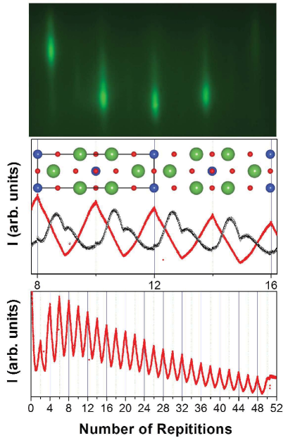
The growth sequence starts with the deposition of a La layer followed by a Cu layer. In situ control of the layer-by-layer growth is provided by Reflection High Energy Electron Diffraction (RHEED) patterns acquired during the growth process (top image of Fig. 1). After the deposition of the La layer a three-dimensional (3D) RHEED pattern, characteristic of a rough surface, can be observed. Once the deposition of the Cu layer is finished, the characteristic scattering rods of a two-dimensional (2D) growth are revealed indicating the presence of a flat surface (see top image of Fig. 1). In the bottom graph of Fig. 1 we show the RHEED oscillations obtained from the integrated intensity over the area of the specular rod during the growth of a 12.5 unit cell thick sample. Note that the time units of the X axis of this graph have been scaled to the number of times that the La and Cu shutters were opened. The count starts at zero which corresponds to the first La deposition, and so, the odd (even) numbers in the X axis of Fig. 1 correspond to the closing (opening) of the La shutter and the opening (closing) of the Cu shutter. The RHEED oscillations reveal that the growth method succeeds in preserving a smooth sample surface up to the thickest (300 A) films that were grown. Moreover, one can follow the growth by counting the number of single atomic planes of each element deposited. The middle graph of Fig. 1 shows a detail of the same growth corresponding to the deposition of the 4th and 5th unit cells of the film. The black line in the figure is obtained by integrating the intensity of the small spot that is characteristic of the 3D growth of the RHEED pattern during the La and Cu deposition. It reveals the formation of two LaO planes that takes place before the completion of half of a single unit cell. The picture shown on top of this graph is a guide to following the growth sequence and it is a sketch of the crystallographic structure of LCO.
III.2 Structural characterization of the LCO thin films
The structural characterization of the films has been carried out by means of X-Ray Diffraction and Atomic Force Microscopy (AFM). In Fig. 2 we show the X-Ray results obtained for a set of characteristic samples. Figure 2A shows the X-Ray Reflectivity (XRR) patterns of 12.5, 12, 4 and 4 unit cell thick LCO films grown on STO, SLAO, STO and SLAO substrates respectively, from top to bottom. Finite size thickness oscillations corresponding to the total thickness of the film can be clearly observed over a wide range of values of 2. The presence of interference fringes indicates that both the substrate-sample and sample-air interfaces are flat and smooth. A quantitative analysis of the XRR results was carried out using GenX software.Björck and Andersson (2007) The refinement results, the red lines in Fig. 2A are in agreement with the nominal thicknesses observed during the growth using the RHEED technique. We obtain a roughness of the sample-substrate interface of less than 2 A, as well as a sample-air interface roughness of about 6 A which are in good agreement with the height of half a unit cell. Both values of roughness are the same for all of the samples.
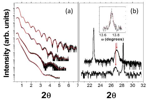
The Wide Angle X-Ray Diffraction data (Fig. 2B) show that the sample is grown textured in the (0 0 1) crystallographic direction of the substrate with high crystalline quality. (From top to bottom we show the data for the 12.5 and 12 unit cell samples grown on STO and SLAO respectively.) No peaks of secondary phases can be seen over the whole scan (12 < 2 < 65) but peaks corresponding to the (0 0 n) family of crystallographic planes of both the substrates and -LCO thin films are observed. As marked with red arrows in Fig. 2B, the position of the (0 0 4) Bragg peak of the thin film depends strongly on the substrate used for the growth. As expected for growth on a SLAO substrate, an in-plane compressively strained thin film with a c-axis lattice parameter c = 13.3 Å is obtained.
The presence of ozone and the compressive strain result in the formation of a -LCO thin film where the unit cell volume is not preserved and a non-stoichiometric superconducting phase with excess of oxygen is stabilized instead of the insulating antiferromagnetic stoichiometric LCO phase. The introduction of oxygen interstitials at the La2O2+δ spacer layers together with the compressive strain produces an expansion of the unit cell in the out-of-plane direction and turns the sample into a high TC superconductor. The samples grown on STO are tensile strained and have a c-axis parameter of 13.2 Å. With the samples grown on STO we checked that the oxidizing atmosphere by itself was able to stabilize -LCO regardless of the strain state induced in the thin film. In the inset of Fig. 2B we show the rocking curve corresponding to the (0 0 4) Bragg peak of the 12 unit cell thick film as a representative example. The full width at half maximum (FWHM) of the peak is 0.03 degrees which indicates the very low mosaicity of our samples and the structural coherence of the thin film in the direction of the growth.
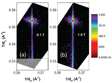
We use reciprocal space maps (RSM) to get access to the in-plane lattice parameters of the sample. In order to check both the a and b lattice parameters, we map the off-specular (1 0 7) and (0 1 7) H and K directions of the RS respectively. The results for a 4 unit cell thick film grown on SLAO are exhibited in Fig. 3, which shows the out-plane (L) direction of the RS plotted vs. the in-plane one. (Fig. 3A corresponds to the K direction and Fig. 3B corresponds to the H direction.) The intense peak in both maps corresponds to the SLAO substrate reflection while the thin film reflection is the wide (narrow) maximum along the Y axis (X axis). The maps confirm that the sample is epitaxial and are evidence of an in-plane coherence length of the thin film limited by the substrate in-plane coherence length. The wide thin film peak in the L direction is a consequence of the finite size thickness (~ 5.5 nm) of the sample.
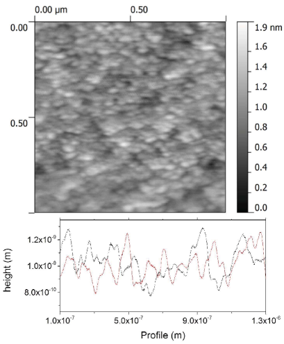
Figure 4A shows a 1 m 1 m AFM scan of the 4 unit cell film. The average root mean square roughness, rms is 0.2 nm, which is strictly the same as that obtained for the 10 m 10 m scans. The thickness variation relative to the total thickness of the sample is 3.75 %. In Fig. 4B the height profile scans obtained from the main diagonals of the image can be observed. They reveal that the largest height variation is 4 Å, which corresponds to a third of a -LCO unit cell. The surface roughness of the thin film matches the surface roughness of the SLAO substrate after it is annealed under conditions equivalent to those of the growth.
IV Electronic Double Layer Transistor fabrication and operation
All the set of transport experiments described in this work were carried out using the same EDLT. The device was fabricated using a 4 unit cell (5 nm) thick film of -LCO. To preserve the sample surface during the fabrication of the device, the cuprate film was kept in an inert N2 gas atmosphere inside a small portable vacuum chamber. When procedures open to the atmosphere were required, a continuous flow of the same gas was used to minimize the exposure of the surface to moisture, CO2 and other atmospheric gases that would potentially degrade the surface quality of the thin film. Silver electrodes were deposited on the four corners of the thin film to allow us characterize its electrical transport properties. The electrodes were deposited by a thermal evaporation method and during this process the sample was kept at liquid N2 temperature to avoid the de-oxygenation of the thin film. As sketched Fig. 5a, the sample with the deposited electrodes was mounted in a glass cylinder that contains the DEME-TFSI ionic liquid used as the gate dielectric. Electrical wires were attached to the Ag electrodes with indium dots and a Pt coil (gate electrode) was installed on the top of the device.
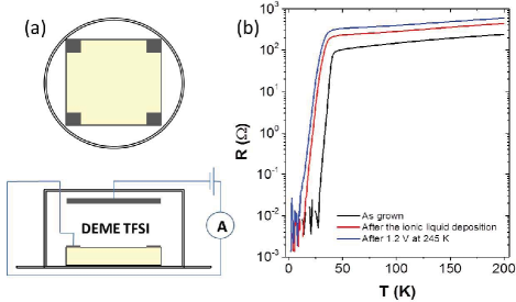
In Fig. 5b we show the evolution of the R(T) curves of LCO film during the fabrication and optimization of the device. Before applying the ionic liquid to the surface of the film, and after the above described manipulation, the as-grown sample has a R(T) curve characteristic of a high quality -LCO crystal. The superconducting transition temperature (TC) of the sample is 45 K which is the highest TC reported for thin films of this thicknessBozovic et al. (2002) or for the bulk form of this material.Chou et al. (1992) Once the ionic liquid is added to the cylinder glass container we again measured R(T) of the film (red curve). There is a drop in the onset temperature of the superconducting transition of about 10 K and the transition becomes broader. The ionic liquid is added at room temperature and we cannot avoid what appears to be a slow room temperature chemical degradation of the sample surface, which is completely arrested when the sample is cooled down to the gating temperatures (240-245 K). We start electrostatically charging the -LCO film at 240 K by applying positive gate voltages (VG) that induce negative charges in the film, and therefore, reduce its carrier concentration. The gating process at this temperature and up to 1.2 V does not produce any significant change in the normal state resistance and does not affect TC . In order to build up more charge on the sample surface and enhanced the charge transfer to the sample, we increased the ionic mobility by increasing the gating temperature to 245 K. After recovering the previous VG, i.e. 1.2 V, the normal state resistance of the sample had increased by a factor of 1.5, and TC dropped more than 1 K (the blue line in Fig. 5B). Subsequently, all the different values of VG or hole concentration presented in this work were obtained after gating the sample at 245 K over a period of 10-15 min.
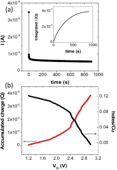
In order to monitor the electrostatic charging of the sample, we measured the charge leakage current between the Pt coil and the sample during the gating process with the configuration illustrated in the bottom panel of Fig. 6a. A Keithley 6517 electrometer was used as both the in-series voltage source and as a picoammeter. An example of the leakage current vs. time measurements is shown in Fig. 6a. After removing the constant background which appears for the longer times of the measurement, we integrated the curves as a function of time to estimate the amount of charge transferred to the sample in each charging step (see the inset of Fig. 6a). This allows us to calculate the total accumulated charge for each increment of gate voltage. These are the red symbols in Fig. 6b. Finally, the concentration of holes at the -LCO thin film for each VG (black symbols of Fig. 6b) can be derived by assuming that the initial concentration of holes per superconducting oxygen plane (holes/Cu) is given by the Hall number of the initial VG measured at 190 K. The initial density of holes for the 1.2 V gated thin film at 245 K is 0.1215 holes/Cu and this is in good agreement with the estimation of the number of holes obtained from the parabolic relationship between TC and the hole concentration for the same conditions.Tallon et al. (1995) However, we would like to clarify that this is not an accurate estimation of the absolute value of charge density in the film, but it allows us to estimate the relative evolution of carrier concentration with VG.
V Transport and magneto-transport measurements. Results and Discussion
The electrical resistance of the sample was measured using a four-terminal configuration employing the following devices: a Keithley 7001 switching system, a Keithley 6221 current source and a Keithley 2182A nanovoltmeter. The temperature of the device and the magnetic field conditions of the measurement were controlled in a Physical Properties Measurement System (PPMS).
We designed an experiment to access three different measurement configurations of the in-plane resistance based on a four-terminal transport experiment. The first two resistance configurations were obtained by applying the electrical current in the main tetragonal in-plane crystallographic directions of the film that coincide with the edges of the sample. We denote these resistances as R1 and R2, as well as their sheet resistance counterparts as Rs1 and Rs2 respectively. In order to determine the values of sheet resistance along the main crystallographic directions of the -LCO thin film (Rs1 and Rs2) from R1 and R2, we applied the method explained in the reference.dos Santos et al. (2011) The method is a revision of the Montgomery method,Montgomery (1971) and it allows us to determine the 2D electrical sheet resistance tensor of the tetragonal structure of the -LCO thin film. The third resistance was the Hall Resistance denoted by Rxy. We have characterized the three resistances in zero field and in a 9 T applied magnetic field. This measurement configuration allows us to obtain the ratio Rs1/Rs2, which will be used to evaluate the in-plane anisotropy of the electrical properties.
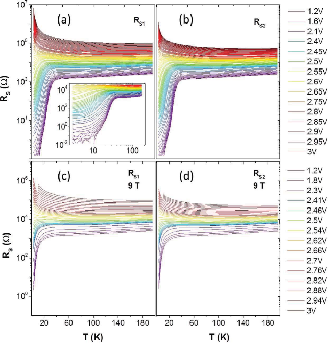
Figure 7 shows a false color plot of the dependence on temperature of Rs1 and Rs2 from 3 K to 200 K for different values of VG for both 0 T and 9 T magnetic fields. The different values of VG range from 1.2 V (purple or cold) to 3 V (brown or hot) corresponding to a concentration of holes per copper oxygen plane of 0.1215 holes/Cu and (-0.00625) holes/Cu respectively. Figures 7a and 7c show the data obtained for Rs1 in zero field and in a 9 T magnetic field, respectively, and Figs. 7b and 7d show the results obtained for Rs2 under the same field conditions. We display a total of 75 different values of VG, i.e. doping levels, for the data obtained without magnetic field (for both Rs1 and Rs2) and 33 values of VG for the sets of data taken at 9 T. The legend displays the color code for some representative values of VG.
As can be seen in Fig. 7, both curves of and show a characteristic evolution from superconducting to insulating behavior as VG is increased and the charge carrier concentration is depleted. For VG=1.2 V, the sample is metallic down to the superconducting transition temperature TC40 K for the 0 T data and down to TC25 K for the 9 T data. With a further increase of VG the transition temperature slowly moves towards lower temperatures as expected for the depletion of holes in the superconducting CuO2 planes. Below 40 K (25 K) the transition is continuous and the corresponding gate voltage that separates the superconducting and insulating regimes is VG=2.64 V (VG=2.54 V) for the measurements obtained with a 0 T (9 T) magnetic field. Under 0 T and 9 T conditions of applied magnetic field, Rs1 and Rs2 show a similar evolution with VG.
V.1 Finite size scaling
These data of resistance vs. temperature at different gate voltages resemble that of the reported continuous SITs as a function of charge carrier concentration in the cuprates YBa2Cu3O7-δLeng et al. (2011) and La2-XSrXCuO4.Bollinger et al. (2011) Continuous SITs are quantum phase transitions (QPTs) with quantum critical points separating the superconducting and insulating ground states. Near the QCP and at nonzero temperature the different phases are separated by a Quantum Critical Regime (QCR). In the QCR, the dependence of a macroscopic observable property, Rs, as a function of the tuning parameter, the concentration of holes per superconducting CuO2 plane (p), should follow a scaling law of the form:
| (1) |
Here and are the critical sheet resistance and the critical carrier concentration respectively, T is the temperature and is the critical exponent product that characterizes the universality class of the phase transition.Sondhi and Shahar (1997)
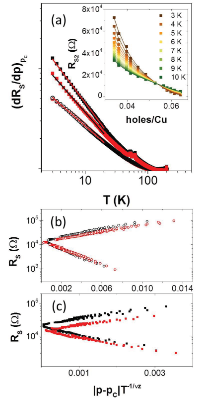
Following the procedures described in the reference,Marković et al. (1999) we first obtained the critical values of carrier concentration for the four different configurations of the experiment. After plotting Rs as a function of p for the lower temperature isotherms of the experiment (3-10 K), we found a crossover, which is the value of the temperature independent sheet resistance at critical doping, . (See the inset of Fig. 8a as an example.) The value of for the 0 T measurements is 0.04 holes/Cu and for the 9 T measurements is 0.055 holes/Cu. It is independent of the in-plane direction of the measurements. We then obtain by the evaluation of the derivative of Rs with respect to p at . This procedure involves the fitting of all the isotherms of the study by a polynomial function that accurately takes into account the curvature of the data at this point. The results of the polynomial fit are the lines plotted in the inset of Fig. 8a. We then obtain the critical exponent product of the transition as the negative of the inverse of the slope of the straight line yielded from the log-log plot of vs. . This is shown in Fig. 8a along with the linear fits to the data. Interestingly we obtained two different values of for the 0 T measurements: =1.2 for Rs1 and =1.4 for Rs2, while the transition under a 9 T magnetic field is characterized by a single value of for both directions of the applied electric field: = 1.8. As can be observed in Fig. 8a, this method is a sensitive tool for determining , allowing us to distinguish between small variations of the slope. Moreover, it allows us to estimate the upper temperature limit of the QCR as the temperature at which the analysis deviates from the linear regime. Surprisingly, the quantum fluctuations persist up to approximately 30 K.
From the previous analysis of the data we obtain the values of RsC. The critical value for Rs1 / 0 T (Rs2 / 0 T) is approximately 21.5 k (15 k), and for Rs1 / 9 T (Rs2 / 9 T), RsC decreases to 13.5 k (12.5 k). The measured values of RsC do not agree with the quantum resistance for pairs (6.45 k). The result supports the possibility of a QPT driven anisotropically in the absence of magnetic field and isotropically in its presence.
An alternative method for determining the critical exponent product of the transition is to obtain the best collapse of the Rs data inside the QCR onto the scaling function.Marković et al. (1999) In Figs. 8b and 8c we show the results of this analysis for the 0 T and 9 T transitions respectively. It highlights the collapse of the data as well as the agreement of the values of the critical exponents obtained by the two independent methods. This analysis suggests that there is a direct SIT between superconducting and insulating regimes with the caveat that the analysis is cut off at a relatively high temperature leaving open the possibility of a more complex scenario at temperatures below those actually measured. Indeed, a closer inspection of the curves reveals that zero resistance is only achieve for the few highest doping levels (see inset of Fig. 8a). Otherwise, the low temperature resistance of the sample saturates reaching a constant value different from the expected 0 of the superconducting state. This result could be a consequence of the occurrence of quantum fluctuations that would prevent the system from becoming superconducting above 0 K and that would be enhanced by the 2D character of the sample.Yen-Hsiang Lin and Goldman (2012)
The SIT in 2D has been the focus of many experimental and theoretical works for several years. These include studies of amorphous Bi,Parendo et al. (2005) amorphous MoGe,Yazdani and Kapitulnik (2000) InOX,G. Sambandamurthy and Shahar (2004) TiN,Baturina et al. (2005) STO,Caviglia et al. (2008) and more recently in LSCO,Bollinger et al. (2011) YBCOLeng et al. (2011) and FeSe.R. Schneider and v. Lohneysen (2012) To our knowledge there has not been any previous report of a possible anisotropic QPT that, moreover, becomes isotropic under an applied magnetic field. This result would imply that there is an intrinsic electronic anisotropy in the sample that drives the quantum phase transition with a different mechanism depending on the in-plane direction. A magnetic field perpendicular to the CuO2 planes is able to suppress the anisotropy suggesting a link between the superconducting state and the anisotropy. To further explore this phenomenon we characterized the in-plane anisotropic electronic properties of the sample by means of the coefficient Rs1/Rs2.
V.2 In plane anisotropy of the sheet resistance
Figures 9a and 9b show false color contour plots of the ratio Rs1/Rs2 as a function of carrier concentration and temperature for the data obtained in zero field and in 9 T. In both maps, cold colors (violet) represent a value of Rs1/Rs2=1, with the value of Rs1/Rs2 increasing with the increase of the color temperature up to a maximum value Rs1/Rs2=5.4 (red.) It is shown that the electrical resistance of the sample in the absence of magnetic field is isotropic in-plane for a wide range of temperatures and hole carrier concentrations. For the highest level of doping, p0.12 holes/Cu, anisotropy appears once the sample is cooled down to TC. As the charge density decreases, the intensity of the anisotropy increases and shifts towards lower temperatures following the line of the superconducting dome. At the high carrier concentration and low temperature portion of the color map, Rs1/Rs2 reaches a maximum value of 4 at p=0.06 holes/Cu and T=3 K. With further depletion of holes, the intensity of the anisotropy falls and it achieves a minimum at the critical carrier concentration of holes for the SIT and at the lowest temperature of the experiment, i. e., p=0.04 holes/Cu and T= 3K. From this point downward to the lowest carrier concentrations the anisotropy continuously increases up to the highest value Rs1/Rs2=5.5, deep inside the insulating regime. In this region of doping the anisotropy is present up to 200 K and it decreases as the temperature increases.
After applying a 9 T magnetic field perpendicular to the CuO2 planes (Fig. 9b), the anisotropy of the high charge density part of the color map is shifted downward, disappearing from the temperature window of the experiment, in a similar manner to the suppression of TC. Interestingly, the rest of the contour plot remains strictly the same as the one obtain for 0 T and the only differences emerge after cooling the sample below 40 K (The coefficient of both Rs1/Rs2 obtained with 0 and 9 T is shown in Fig. 9c.)
The presence of in-plane anisotropy in the transport properties is a striking result. The anisotropy is developed at the superconducting transition which probably is enhancing the sensitivity of its detection. Moreover, the presence of anisotropy would imply that the macroscopic symmetry of the sample must be broken in order to set a preferential channel for conductance along one of the Cu-O-Cu directions. In this regard, the structural characterization of the sample has not revealed any structural or morphological difference along the a and b directions of the thin film. Neither AFM nor X-Ray experiments suggests this possibility. However, we have no tool to characterize the oxygen interstitial order in the ultra-thin film and we may be missing an important piece of information.
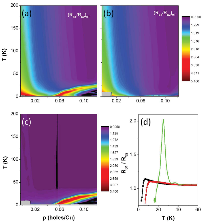
The observation of a quantum SIT that behaves differently depending on the in-plane direction, together with the emergence of an in-plane anisotropy in the electrical properties of the sample, is evidence that the electronic ground states of -LCO thin films are intrinsically anisotropic on both sides of the QCP. Inside the QCR, the quantum fluctuations between both regimes become more important. They eventually result in a reduction of the electronic anisotropy and the system correspondingly becomes more isotropic as it becomes more quantum in nature (i.e. Rs1/Rs2 decreases as we approach the QCP.)
One of the possible ways of interpreting the existence of a preferred conductance channel in the system can be done in terms of the models of electronic and spin orderings and the experimental observations of stripe formation in the 214 family of cuprates.Berg et al. (2009) In this scenario, the charge that dopes an antiferromagnetic Mott insulator it is not randomly distributed in the sample. It forms ordered clusters of charge and spins promoted by antiferromagnetic correlations and charge density modulations. The interlocked patterns can vary from a “classical crystal (CC)” order of charge on the insulating side, to “quantum electronic liquid crystal phases (QELC)” or charge or spin density waves in the superconducting regime.Kivelson et al. (1998) In this regard, neutron scattering experiments on stage 4 and 6 -LCO single crystals have shown that a spin density wave state appears at the superconducting transition temperature, which is enhanced with a perpendicular applied magnetic field, contrary to our observations on electrical anisotropy in field.Khaykovich et al. (2003) In the system under study, the 2D character of the ultrathin film could be enhancing the essential 2D character of the superconducting CuO2 planes, which may result in a 1D chain clustering of holes. Accordingly, stripe formation could produce a lower resistance channel for current flowing along the chains of holes than for current flowing across them.
The comparison of data with and without magnetic field is evidence that the nature of the electronic ground states on the insulating and superconducting sides are different depending upon the magnetic field. On the one hand, at the lower levels of doping the anisotropy is more stable and the 9 T field barely has any effect on its temperature and charge density dependences. These results suggest that the lightly doped insulating state could be antiferromagnetic, as might be expected from the bulk behavior, and a long-range exchange interaction of spins would stabilize robust charge and spin orderings, independent of magnetic field. On the other hand, the effect of magnetic field on the superconducting side reduces the intensity of the anisotropy significantly and it only appears at the lowest temperatures. This result could be a consequence of the reduction of TC. As stated earlier, the superconducting transition could be enhancing the sensitivity of detection and the presence of the anisotropy in other regions of the phase diagram could pass unnoticed. Nevertheless, the effect of magnetic field on the anisotropy is evidenced in Fig. 9d. Here we have plotted the value of Rs1/Rs2 for p=0.1215 holes/Cu measured with 0 T (green line), 4.5 T (red line), -4.5 T (red squares), 9T (black line) and -9 T (black squares) as a function of temperature. The anisotropy is developed only in the absence of field and is not correlated with the transition temperature, which is shifted systematically to lower temperatures with the increasing field. We suggest that the anisotropy could arise due to electronic inhomogeneity and the possibility of strong spin-orbit scattering in a highly 2D system could lead to the magnetic response of the anisotropy. However, there is neither a specific model for the anisotropy in the conductance of the thin film, nor a model for its response to magnetic field.
V.3 Hall Resistance
In order to characterize the temperature and doping dependence of Rxy of the LCO thin film, we measured the Hall voltage (VH) with a 9 T applied magnetic field. We did this for both positive and negative currents across both of the diagonal contacts of the four-terminal configuration when the current was applied in the opposite diagonal. The same measurements were also carried out without magnetic field, to check the zero value (see Fig. 10a), and with 9 T during the warming of the sample from 3 K to 200 K. Accuracy tests under -9 T, -4.5 T and 4.5 T were measured at selected carrier concentrations as a control parameter of the experiment (see Fig.10b). This was also done in resistance vs. magnetic field sweeps. The data confirm the linear dependence of Rxy on magnetic field and that the sensitivity of the measurement of 0.1 .
Figure 10b shows the temperature dependence of Rxy for different levels of doping ranging from 0.12 holes/Cu (violet line) to 0.04 holes/Cu (brown line). Over the complete range of carrier concentrations, Rxy increases with decreasing temperature up to a maximum value. Upon further cooling below the maximum region (T 15 K) and depending on whether the sample becomes a superconductor or an insulator, the value of Rxy keeps dropping or eventually increases. It is important to note that the change of to a negative slope at the lowest levels of doping and temperatures is correlated with non-zero values of Rxy measured without magnetic field, and therefore is not meaningful. We have further explored the previous result and obtained the maximum position for each of the curves as well as for each isotherm. These data are displayed in the inset of Fig. 10b and show that the Hall resistance has a maximum at 0.04 holes/Cu at a temperature of 70 K.
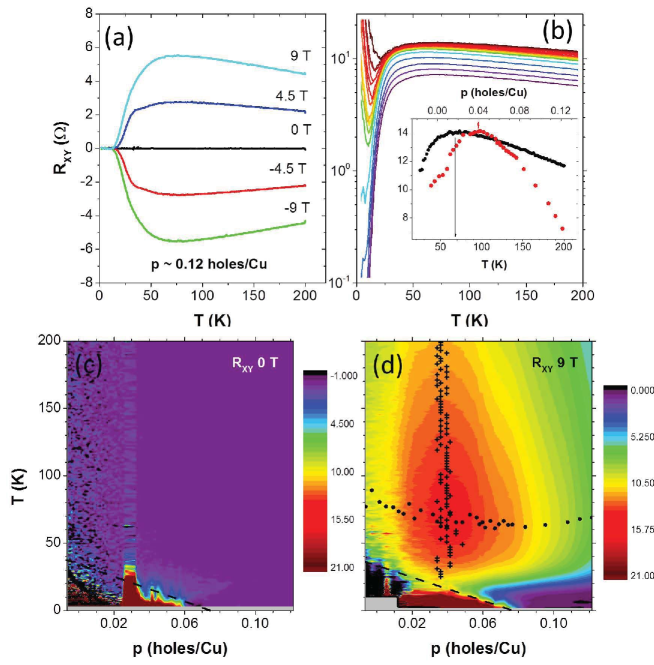
To better visualize this surprising result we show a contour color plot of the Rxy measurements in the temperature-charge concentration plane (Fig. 10d). Note that the purple colors are assigned to Rxy0 . As a result, Rxy measured with a 9T applied magnetic field has a drop-like shape with the maximum values of Rxy represented in red and located around the 0.04 holes/Cu-70 K point. Moreover, by using this representation we can follow the evolution of the maximum of Rxy in the T-p plane. The results reveal that the position of the maximum as a function of p (the cross symbols in Fig. 10d) for the different isotherms is roughly linear with a small shift to lower p as the charge density decreases (from p=0.04 holes/Cu at the lowest temperatures to p=0.035 holes/Cu at 200 K). When the maximum is evaluated as a function of T for the different p values, it is a curve shape with a minimum corresponding to p0.08 holes/Cu at T60 K.
The presence of a maximum in the Hall resistance could be revealing an electronic phase transition,LeBoeuf et al. (2011)Leng et al. (2012)Balakirev et al. (2003) which is a surprising and interesting result. The surprise comes from the fact that the maximum value of Rxy is found at the critical carrier concentration for the SIT at 0 T and the QPT would be a consequence of an electronic transition which occurs even at high temperature. At the temperatures where the maximum is observed, we have found that the longitudinal resistances measured with 0 T and 9 T are strictly the same. Hence, the Rxy maximum is evidence of a phenomenon that promotes the QPT at 0 T. The interesting implication of this discovery is that the SIT in electrostatically doped -LCO would be driven by electronic interactions since it would involve a change in the electronic properties of the system when it transitions from the insulating to the superconducting phases. This scenario is further support by the presence of a minimum in the anisotropy of the electrical transport properties at the QCP.
VI Conclusions
The results presented here highlight the role that electronic interactions play in the transition from the superconducting state to the insulating regime. The low temperature transport scales down to the lowest temperature of the experiment, which suggests a possible QPT that is anisotropic without magnetic field and isotropic in the presence of a 9 T field. The electronic nature of this anisotropy is reveal by the measurements of the coefficient Rs1/Rs2, which interestingly are minimized at the critical concentration of charge carriers of the SIT. Furthermore, at this concentration of holes we have found a maximum in the Hall resistance at high temperature that could be revealing the electronic nature of the low temperature transition.
Acknowledgements.
We thank the late Zlatko Tesanovic, Guichuan Yu, Wojciech Tabis, Shameek Bose, Rafael Fernandes, Brian Skinner, Boris Skhlovskii, Steve Kivelson, Vlad Dobrosavljevic, Marcello Rozenberg, Carlos Leon and Jacobo Santamaria for helpful discussion; we also thank Chad Geppert for his help with transport measurements. This work was supported by the National Science Foundation under Grants No. NSF/DMR-0854752 and NSF/DMR-1209678. Part of this work was carried out at the University of Minnesota Characterization Facility, a member of the NSF-funded Materials Research Facilities Network via the MRSEC program. J. G. B. thanks the financial support through the Ramon y Cajal Program.References
- Leggett (2006) A. J. Leggett, Nature Phys. 2, 134 (2006).
- Lee and Wen (2006) P. a. Lee and X.-G. Wen, Rev. Mod. Phys. 78, 17 (2006).
- Varma (2010) C. Varma, Nature 468, 184 (2010).
- Orenstein and Millis (2000) J. Orenstein and A. J. Millis, Science 288, 468 (2000).
- Sondhi and Shahar (1997) S. L. Sondhi and D. Shahar, Rev. Mod. Phys. 69, 315 (1997).
- Fisher (1990) M. P. Fisher, Phys. Rev. Lett. 65, 923 (1990).
- Anderson (1986) P. W. Anderson, Science 235, 1196 (1986).
- Shimotani et al. (2007) H. Shimotani, H. Asanuma, A. Tsukazaki, A. Ohtomo, M. Kawasaki, and Y. Iwasa, Appl. Phys. Lett. 91, 082106 (2007).
- Ye et al. (2010) J. T. Ye, S. Inoue, K. Kobayashi, Y. Kasahara, H. T. Yuan, H. Shimotani, and Y. Iwasa, Nature Mater. 9, 125 (2010).
- Lee et al. (2011) Y. Lee, C. Clement, J. Hellerstedt, J. Kinney, L. Kinnischtzke, X. Leng, S. Snyder, and A. Goldman, Phys. Rev. Lett. 106 (2011).
- Kastner et al. (1998) M. Kastner, R. Birgeneau, G. Shirane, and Y. Endoh, Rev. Mod. Phys. 70, 897 (1998).
- Imada et al. (1998) M. Imada, A. Fujimori, and Y. Tokura, Rev. Mod. Phys. 70, 1039 (1998).
- Wells et al. (1997) B. O. Wells, Y. S. Lee, M. A. Kastner, R. J. Christianson, R. J. Birgeneau, K. Yamada, Y. Endoh, and G. Shirane, Science 277, 1067 (1997).
- Lee et al. (1999) Y. Lee, R. Birgeneau, M. Kastner, Y. Endoh, S. Wakimoto, K. Yamada, R. Erwin, S.-H. Lee, and G. Shirane, Phys. Rev. B 60, 3643 (1999).
- Fratini et al. (2010) M. Fratini, N. Poccia, A. Ricci, G. Campi, M. Burghammer, G. Aeppli, and A. Bianconi, Nature 466, 841 (2010).
- C. Chaillout, S.W. Cheong , Z. Fisk , M.S. Lehmann , M. Marezio J and Schirber (1989) B. M. C. Chaillout, S.W. Cheong , Z. Fisk , M.S. Lehmann , M. Marezio J and J. Schirber, Physica C 158, 183 (1989).
- Eisaki et al. (2004) H. Eisaki, N. Kaneko, D. Feng, a. Damascelli, P. Mang, K. Shen, Z.-X. Shen, and M. Greven, Phys. Rev. B 69, 1 (2004).
- Berkley et al. (1989) D. D. Berkley, A. M. Goldman, B. R. Johnson, J. Morton, and T. Wang, Rev. Sci. Instrum. 60, 3769 (1989).
- Björck and Andersson (2007) M. Björck and G. Andersson, J. Appl. Cryst. 40, 1174 (2007).
- Bozovic et al. (2002) I. Bozovic, G. Logvenov, I. Belca, B. Narimbetov, and I. Sveklo, Phys. Rev. Lett. 89, 4 (2002).
- Chou et al. (1992) F. Chou, J. Cho, and D. Johnston, Physica C 197, 303 (1992).
- Tallon et al. (1995) J. L. Tallon, C. Bernhard, and H. Shaked, Phys. Rev. B 51, 911 (1995).
- dos Santos et al. (2011) C. a. M. dos Santos, A. de Campos, M. S. da Luz, B. D. White, J. J. Neumeier, B. S. de Lima, and C. Y. Shigue, J. of Appl. Phys. 110, 083703 (2011).
- Montgomery (1971) H. C. Montgomery, J. of Appl. Phys. 42, 2971 (1971).
- Leng et al. (2011) X. Leng, J. Garcia-Barriocanal, S. Bose, Y. Lee, and A. Goldman, Phys. Rev. Lett. 107 (2011).
- Bollinger et al. (2011) A. T. Bollinger, G. Dubuis, J. Yoon, D. Pavuna, J. Misewich, and I. Božović, Nature 472, 458 (2011).
- Marković et al. (1999) N. Marković, C. Christiansen, A. Mack, W. Huber, and A. Goldman, Phys. Rev. B 60, 4320 (1999).
- Yen-Hsiang Lin and Goldman (2012) J. N. Yen-Hsiang Lin and A. M. Goldman, Phys. Rev. Lett. 109, 017002 (2012).
- Parendo et al. (2005) K. A. Parendo, K. H. Sarwa B Tan, A. Bhattacharya, M. Eblen-Zayas, N. E. Staley, and A. M. Goldman, Phys. Rev. Lett. 94, 1 (2005).
- Yazdani and Kapitulnik (2000) A. Yazdani and A. Kapitulnik, Phys. Rev. Lett. 74, 3037 (2000).
- G. Sambandamurthy and Shahar (2004) A. J. G. Sambandamurthy, L.W. Engel and D. Shahar, Phys. Rev. Lett. 92, 10 (2004).
- Baturina et al. (2005) T. I. Baturina, A. Mironov, V. Vinokur, M. Baklanov, and C. Strunk, Phys. Rev. Lett. 99, 1 (2005).
- Caviglia et al. (2008) A. D. Caviglia, S. Gariglio, N. Reyren, D. Jaccard, T. Schneider, M. Gabay, S. Thiel, G. Hammerl, J. Mannhart, and J.-M. Triscone, Nature 456, 624 (2008).
- R. Schneider and v. Lohneysen (2012) D. F. R. Schneider, A. G. Zaitsev and H. v. Lohneysen, Phys. Rev. Lett. 108, 257003 (2012).
- Berg et al. (2009) E. Berg, E. Fradkin, S. A. Kivelson, and J. M. Tranquada, New J. Phys. 11, 115004 (2009).
- Kivelson et al. (1998) S. A. Kivelson, E. Fradkin, and V. J. Emery, Nature 393 (1998).
- Khaykovich et al. (2003) B. Khaykovich, R. Birgeneau, F. Chou, R. Erwin, M. Kastner, S.-H. Lee, Y. Lee, P. Smeibidl, P. Vorderwisch, and S. Wakimoto, Phys. Rev. B 67, 1 (2003).
- LeBoeuf et al. (2011) D. LeBoeuf, N. Doiron-Leyraud, B. Vignolle, M. Sutherland, B. J. Ramshaw, J. Levallois, R. Daou, F. Laliberte, O. Cyr-Choiniere, J. Chang, et al., Phys. Rev. B 83, 054506 (2011).
- Leng et al. (2012) X. Leng, J. Garcia-Barriocanal, B. Yang, Y. Lee, J. Kinney, and A. Goldman, Phys. Rev. Lett. 108, 1 (2012).
- Balakirev et al. (2003) F. F. Balakirev, J. B. Betts, A. Migliori, S. Ono, Y. Ando, and G. S. Boebinger, Nature 424, 912 (2003).