Embedded Boron Nitride Domains In Graphene Nanoribbons For Transport Gap Engineering.
Abstract
We numerically investigate the impact of boron nitride (BN) domains on the transport properties of graphene nanoribbons with lengths ranging from a few to several hundreds of nanometers and lateral size up to 4 nm. By varying the size and morphology of the BN islands embedded in the graphene matrix, a wide transport tunability is obtained from perfect insulating interfaces to asymmetric electron-hole transmission profiles, providing the possibility to engineer mobility gaps to improve device performances. Even in the low-density limit of embedded BN islands, transport properties are found to be highly dependent on both the BN-domain shape and the size with a strong tendency toward an insulating regime when increasing the number of ionic bonds in the ribbon. This versatility of conduction properties offers remarkable opportunities for transport gap engineering for the design of complex device architectures based on a newly synthesized one-atom hybrid layered material.
pacs:
72.80.Vp, 73.23.-b, 71.15.Ap, 31.15.E-I INTRODUCTION
Two-dimensional graphene has become a fantastic playground for exploring electronic and transport properties on the nanoscale.Novoselov (2011); Wakabayashi (2001); Yamamoto et al. (2009); Cresti et al. (2008) Among its many spectacular and unique features, charge transport has been found to be weakly sensitive to disorder, owing to quantum mechanisms and interference effects, such as the Klein tunneling and the weak antilocalization phenomenon Katsnelson et al. (2006); McCann et al. (2006); Ortmann et al. (2011), yielding anomalously large charge mobility up to room temperature Bolotin et al. (2008); Du et al. (2008). One limitation of the use of graphene in future nanoelectronics is the absence of an energy band gap, which prevents any efficient electronic current flow from switching off.Roche (2011); Mucciolo et al. (2009) The modification of graphene geometry and chemical structure with selective methods, such as the chemical attachment of functional groups with specific features, allows for mobility gap engineering. Sun et al. (2011); Li et al. (2008, 2009) However, the covalent functionalization of graphene inevitably leads to the creation of defects in the aromatic structure of graphene which eventually yields strong localization phenomena in graphene samples, reducing by orders of magnitude the otherwise large mobilities and associated current densities.
In that perspective, a very appealing strategy to tune electronic features of graphene is to incorporate boron nitride (BN) domains inside the carbon matrix host to create a boron-nitride-carbon (BNC) heterostructure, taking advantage of the isomorphism between the graphene and the two-dimensional hexagonal BN layer, which exhibits a wide band gap on the order of 6 eV. Blase et al. (1995); Arnaud et al. (2006); Watanabe et al. (2004); Nagashima et al. (1995); Pacile et al. (2008) The BN codoping of graphene materials introduces bonds with a marked ionic character which breaks the network symmetry and disrupts the original graphene hyperconjugated -network. Some impact on the electronic and transport properties is thus expected although to date not fully quantified. The successful experimental fabrication of atomic layers of hybridized patches of BN and graphene Song et al. (2010),Ci et al. (2010) could pave the way for controlled tunability of electronic and transport properties. Indeed, a first transport experiment by Song et al. Song et al. (2010) has revealed some anomalous temperature-dependent insulating-to-metal transitions, tentatively assigned to competing and parallel transport mechanisms. The reported mobilities of these hybrid monoatomic layers are limited to typically 10 with a resistance at the Dirac point of the order of , suggesting that the random distribution of BN clusters and associated domain boundaries introduces a considerable source of scattering in the graphene matrix, despite the preservation of the hexagonal geometry.
In this paper, we report a first-principles study of electronic quantum transport properties of disordered graphene nanoribbons (GNRs) modified with boron nitride domains (BNC-NRs). Using a combination of density-functional-theory-(DFT)-based calculations and simulations of mesoscopic electronic transport based on the Landauer-Büttiker (LB) approach, we unveil a broad spectrum of transport features in disordered graphene ribbons with embedded BN patches. We describe transmission profiles ranging from a total insulating behavior to asymmetric electron-hole conducting patterns and sequences of tunneling resonances in the presence of structural defects, such as vacancies inside the BN clusters. Various configurations of substitutional BN domains in graphene nanoribbons are presented, ranging from the co-doping of BN dimers at different sites across the nanoribbon width up to its complete coverage. This will allow us to explore different quantum transport mechanisms, including the quasiballistic, diffusive, or tunneling regimes. For hybrid BNC-NRs with initially large energy gaps, a superimposed BN-induced transport gap develops. The results are related to the BN-domain size and shape. We compare our findings with previous studies concerning the modification of the aromatic properties of GNRs upon chemical modification induced by functional groups. The richness of the obtained properties offers a wide electronic-transport tunability, which is suitable for engineering complex circuitry and device architecture based on such a two-dimensional platform.
II METHODS
The self-consistent calculation of the electronic structure of a hybrid BNC system is performed with the localized orbital basis set of the SIESTA DFT-based code. Ordejón et al. (1996); Soler et al. (2002) Thus a tight-binding-like Hamiltonian which presents the compactness required to study transport properties within the Green’s function formalism is obtained. A double- basis set with additional polarization orbitals is used to optimize the geometry of the hybrid ribbons and compute their electronic structures. The local density approximation (LDA) is adopted for the exchange correlation functional and the Troullier-Martins scheme Troullier and Martins (1991) is used to describe the interaction between ionic cores and localized pseudo-atomic orbitals. Hybrid BNC-NR are modeled within a supercell with an appropiate distance between neighboring cells to avoid spurious interactions. All atoms are relaxed with a force tolerance of 0.01 eV/Å and the unit cell vectors are relaxed with the maximum stress component being smaller than 0.02 GPa. During geometry optimizations a 1x1x8 Monkhorst sampling is adopted in the Brillouin zone for 3.4 nm long ribbons. The numerical integrals are performed on a real space grid with an equivalent cutoff of 300 Ry.
The electronic transport calculations are based on the LB formulation of conductance, which is particularly suitable to study the electron motion along a one-dimensional device channel in between two semi-infinite leads. We consider a phase coherent system formed by a scattering region where charge carriers can be backscattered during their propagation, and two semi-infinite leads in thermodynamical equilibrium with infinitely larger electron reservoirs. Within the LB approach, we calculate the transmission coefficients for a given channel which gives the probability for an electron to be transmitted at a given energy when it quantum mechanically interferes with the BN domains. The conductance is expressed as , where is the quantum of conductance. The transmission coefficients are calculated by evaluating retarded (advanced) Green’s functions of the system,
| (1) |
where are the self energies describing the coupling of the channel to the left (right) lead. These quantities are related to the transmission factor by the Caroli’s formula Caroli et al. (1971):
| (2) |
with . stands for the trace of the corresponding operator.
To obtain the Green’s function of long disordered ribbons, we first calculate the Hamiltonian and overlap matrices of short BNC-NR sections. These sections are then combined in a random fashion with short pieces of pristine ribbon to build up a system with disorder both along the ribbon length and its lateral size. By means of real-space renormalization techniques Markussen et al. (2007); Triozon et al. (2005); López-Bezanilla et al. (2009) we are able to evaluate the transport properties of BNC-NRs with lengths up to L=2m. To avoid any artificial backscattering effects in the region where two ribbon segments match, the supercell in the ab initio calculation is chosen long enough to avoid any interference of the BN domains in the borders where periodic conditions are applied.
III RESULTS
In the following, we will refer to an armchair BNC-NR, composed of P -dimer lines, as P -aBNC-NR. Armchair GNRs are all semiconducting but with different energy band-gap widths. The pristine GNRs corresponding to the two BN-modified BNC-NRs studied here (14-aBNC-NR and 35-aBNC-NR) belong to the GNRs class with small energy band gaps.Son et al. (2006) Their widths are 1.6 nm and 4.1 nm respectively, which is within the reach of experiments. Li et al. (2008, 2009) The 14-aBNC-NR supercells contain 256 atoms while the 35-aBNC-NR supercells contain up to 666 atoms. The dangling -bonds of the edge atoms are passivated by H atoms. It is always observed that the BNC heterostructures preserve the flat geometry of the unmodified graphene independently of the relative composition although variations of the B-N, B-C and N-C bond lengths are observed for the various types of codopings. The insets in the upper panels of Figure 2 are a schematic representations of typical distances between neighbouring C, B, and N atoms, showing that, with respect to the usual 1.42 Å of bulk graphene, N tends to shorten and B to enlarge the bond lenghts with neighbouring C atoms. This bond length variation is specially noticeable for atoms sitting on the edges. Experimental results in carbon nanotubes demonstrated that B and N are likely to codope into a carbon nanotube by substitution of a pair of carbon atoms, which results in BN existing as neighboring atomic pairs in the hexagonal structures.Xu et al. (2008) According to the computed formation energy for the flat BN-codoped C structures tabulated in Table 1, the configurations with B and N atoms in adjacent positions are all energetically more favourable than any of the considered geometries with B and N separated by one or two C atoms, as shown in intermediate panels of Figure 2. Notice that the codoping with both or one of the BN atoms sitting on the edges is always energetically more favourable.
| BN | B-C-N | B-C-C-N | |
|---|---|---|---|
| i) | 0.71 | 2.00 | 2.08 |
| ii) | 0.75 | 2.03 | 2.15 |
| iii) | 0.72 | 1.85 | 1.93 |
| iv) | 0 | 1.29 | 1.34 |
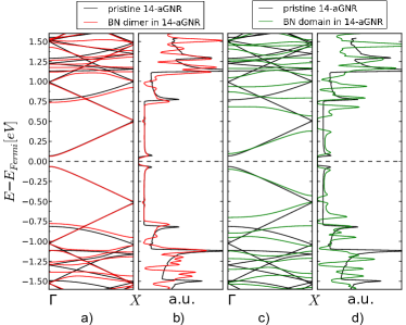
For a better understanding of the effect of BN dimers and larger BN domains in the transport properties of GNR, it is worth comparing the electronic structures of the pristine GNR and the hybrid BNC ribbons. Figure 1 shows an energy band comparison of a pristine 14-aGNR with a 14-aBNC-NR which has a BN dimer located as shown in Figure 2-a)-iii). The presence of a BN pair does not introduce quasibound states, and both the valence and the conduction bands are barely affected by the presence of the impurity. On the contrary, for a larger BN domain, as the one shown in the inset of Figure 5-a), the mixing of B and N electronic states with those of the carbon matrix leads to symmetric small gap openings at energies above eV and below eV the Fermi level, and to a modification of the dispersiveness of the electronic states. In the following, we study the consequence of these electronic structure modifications for long GNRs, containing a varied number of BN defects ranging from 5 up to 320.
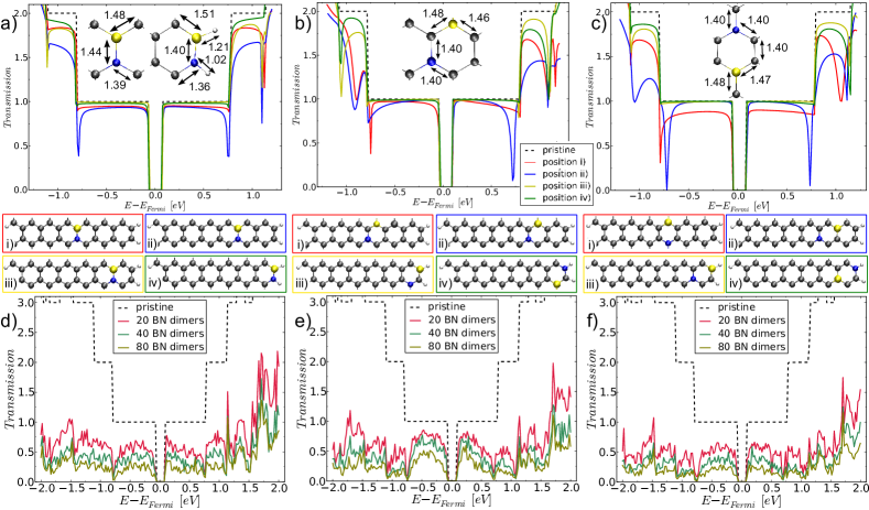
Figure 2 (a,b,c) present a set of transmission profiles for the structures depicted by the corresponding ball-and-stick pictures [from (i) to (iv)] for four different BN pairs in substitutional positions across the ribbon width. The different cases are defined by a varying distance between the doping atoms. The results are strongly position dependent, highlighting the important interplay between co-doping site and edges. For the three types of co-doping, the configurations with one or both B and N atoms sitting on the edge exhibit enhanced robustness against backscattering and, therefore, they are likely to more efficiently preserve the resulting nanoribbon conductance in the presence of disorder. For two adjacent B and N atoms [Figure 2-a], the transmission coefficient drops are almost symmetrically positioned with respect to the Fermi level as also found for BN-co-doped carbon nanotubes Khalfoun et al. (2010) and are related to some Fano-resonance-effect coupling states between different sub-bands (see Ref. Avriller et al. (2007) for details). When B and N atoms are separated by one C atom [Figure 2-b)] or sitting at opposite sites of a hexagon [Figure 2-c)], an asymmetry of backscattering strength between hole and electron channels is observed in the first plateau for some configurations and for all cases in the second plateau. Considering that edge co-doping is energetically more favorable than bulk co-doping, in a controlled growth of BNC-NR, a prevalence of this type of configurations is desirable to preserve charge-carrier mobility against disorder for long GNRs. Therefore, transmission profiles of GNRs containing BN-pair co-doping exhibit a low drop and, in general, a symmetric shape at both sides of the charge neutrality point.
Next, we study each case separately by considering systems with many BN pairs. To simulate realistic systems, we consider random distributions of BN dimers along the length and across the width of 2-m-long aBNC-NRs to analyze how the lack of translational invariance will dictate the electronic-transport regime. The mesoscopic transport calculations are performed introducing 20, 40, and 80 BN dimers randomly distributed along and across the nanoribbon, which represents about 99 in carbon over BN co-doping. Results are shown in panels d)-f), respectively, of Figure 2. It can be noticed that, for a given number of BN pairs, the strength of backscattering is significantly tuned by the separation between B and N dopants from first to third neighboring positions. This is particularly striking for the transmission profile with varying B and N atoms lying at second-nearest neighbor positions [Figure 2-f)] with respect to the others. In this situation, the electronic transport in the first sub-bands clearly appears more stable against BN co-doping. For all cases, the disorder has a larger impact on high-energy sub-bands when compared with the transmission profiles on the first sub-bands, which, even in the low-defect density limit, always remain poorly conducting. The observed behaviors for these sub-bands suggest that the corresponding states are quickly driven to strong localization. For the three types of co-doping and, in particular, for the energetically most favorable cases with adjacent B’s and N’s, an asymmetry between electron and hole conduction develops at high energies. It is worth noticing that BN co-doping is found to yield a weaker impact on the transmission probability when compared with either B doping or N doping, Biel et al. (2009a),Biel et al. (2009b) which can be understood as a compensation effect of the local potential distribution of both atoms in the dimer. Khalfoun et al. (2010)
We now scrutinize the quantum transport properties of the energetically most favorable configurations (adjacent B and N atoms) and compare this type of GNR modification with previous studies based on the total or partial suppression of the orbital of some C atoms as a consequence of the chemical attachment of the functional groups for the ribbon surface. For oxygen atoms in an epoxide configuration, Cresti et al. (2011) the atomic orbitals of two consecutive carbon atoms adopt an intermediate hybridization between and . This results in a weak conductance damage but substantial electron-hole asymmetry of the resulting conductance profiles when considering wide ribbons and low epoxide densities. For a complete hybridization of two opposite C atoms in the hexagonal lattice, Lopez-Bezanilla et al. (2009) the hyperconjugation of the graphitic network is preserved, although the presence of antiresonant states in the first plateau dramatically decreases the transmission ability of the ribbon, turning it into a strong insulator for the small density of grafted atoms (such as H and OH groups) in agreement with Balog et al. (2010). In sharp contrast, BN co-doping appears to impact less markedly on the electronic conductance properties since mean-free paths remain on the order of the micrometer, up to the largest considered BN-co-doping density.
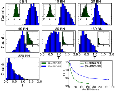
Figure 3 shows the transmission distribution (with as a given disordered sample) for BN-co-doped 35-aBNC-NR (blue) and 14-aBNC-NR (green) at the selected energies with respect to the Fermi levels of 0.3 and 1 eV, respectively. In all cases, B and N atoms are adjacent and are randomly distributed along m-long ribbons. For each histogram, the statistical distribution is performed over 1000 random configurations. The line graphs vs the number of dimers give the evolution of the averaged transmission decay for an increasing BN-co-doping rate in both types of ribbons with values ranging from 5 up to 320 BN dimers. For low BN-dimer density, the statistics is clearly seen to follow a Gaussian distribution around its sample average value , which remains larger than , the quantum of conductance. The transport regime for 35-aBNC-NR (respectively, 14-aBNC-NR) with 10 BN-, 20 BN-, and 40 BN- (respectively, 5 BN-, 10 BN-, and 20 BN-) pair defects randomly distributed along the ribbon axis can, therefore, be described by a quasiballistic or diffusive regime for which , if we denote the ribbon length and the localization length. García-Martín and Sáenz (2001) This allows us to estimate 9 m, 4.4 m and 2.75 m, respectively, for 5 BN-, 10 BN- and 20 BN- pair defects for the 14-aBNC-NR, whereas for the 35-aBNC-NR the values range from 9m down to 3.5m with varying BN dimer number from 10 up to 40. In all cases, the transmission and the localization length are found to roughly decay as ( the number of pairs), in agreement with the Fermi golden rule.Avriller et al. (2007)
When , a crossover is observed and the distribution widens to eventually becomes log-normal for . This behavior turns out to fully agree the universal conductance distributions derived for disordered systems García-Martín and Sáenz (2001), as also found for disordered semiconducting doped nanowires Markussen et al. (2007); Avriller et al. (2007). The transmission fluctuations remain whatever as predicted by the Universal Conductance Fluctuations theorem. This happens to be the case for the 14-aBNC-NR ribbon with 80 BN and 160 BN pairs for which the conductance values and the obtained log-normal distribution (see Figure 3) clearly point towards a localized regime defined by . We obtain =20, 1.2, and 0.8 m for 40 BN, 80 BN, and 160 BN pairs, respectively. The 35-aBNC-NR exhibits stronger robustness to disorder as evidenced by the distribution of the transmission coefficients, which evolves more slowly to a log-normal distribution, being only clearly visible for 320 BN dimers and an average transmission of .
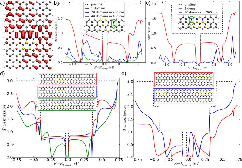
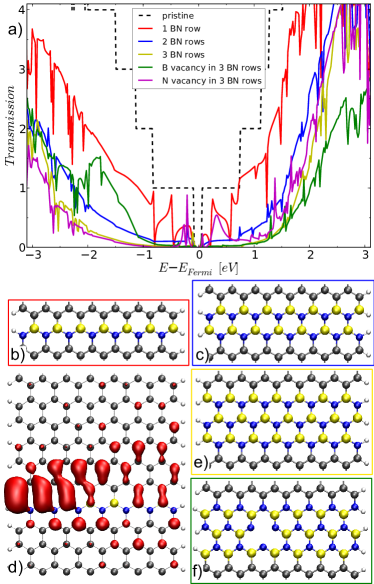
We next investigate the effect on the electron transport of BN barriers of different lengths and bridging two semi-infinite graphene nanoribbons. The main results are summarized in Figure 4. Firstly, a single row of BN pairs covering the whole ribbon width [Figure 4-b)] introduces significant backscattering throughout the considered energy spectrum with a noticeable electron-hole asymmetry. The difference between electron and hole conduction actually increases with Fermi energy in contrast to the prior results of single BN pairs distributed in a random fashion. Additionally, different from the previous case, many resonant states are observed in the first transmission plateau, which retain a high transmission probability. Increasing the number of rows up to 2 and 3 yields a dramatic suppression of charge transport over a large energy window of about 2 eV. This transport gap remains smaller than the energy gap of bulk BN but clearly indicates that the BN barrier acts as an insulating interface, which efficiently filters charge transport. Tunneling effects only persist at higher energies as seen in Figure 4-a). Figure 4-f) shows the efect of a monoatomic vacancyJin et al. (2009); Pochet (2012) introduced in the interface formed by three consecutive BN rows. The presence of both B and N vacancies is found to modify the resonant tunneling regime at specific energies by improving or reducing the transmission probability. See, for instance, the enhanced transmission due to a B vacancy in the energy range from -1 down to -2 eV. Similarly, a N monovacancy in the three BN-row barriers is found to enhance the electron transmission probability in the entire conduction band with respect to the defect-free case. This suggests that both B and N defects in BN patches might create extended states in the domain that can contribute to the ribbon conductivity. All these results show a large tunability of transmission coefficients with the morphology of the BN patches embedded within a graphene ribbon structure. One notes that the presence of resonant states and antiresonances [as illustrated in Figure 4-d) and Figure 4-a) for a chosen energy] for which total reflection or transmission can develop, has been well described for individual dopants in graphene nanoribbons in Ref. Choi et al. (2000).
We now focus on the description of electronic quantum transport properties of GNRs with embedded BN domains composed of an equal number of B and N atoms that remain segregated in the carbon matrix. By tuning the compositional range of the B, N, and C precursors, it is possible to experimentally synthesize layers of graphene with different amounts and sizes of BN domains, Ci et al. (2010) which always segregate inside the graphene layers. Here, we restrict our calculations to small width aBN-NRs to better assess the sensitiveness of electronic transport to both disorder and BN-domain shapes as seen in Figure 5. The two cases studied only differ in the position of a single BN pair, represented with a green oval in the insets of Figure 5-b) and Figure 5-c). The transmission for a single BN patch already shows substantial differences in the first plateau and at higher energies. These differences are further amplified by studying disordered hybrid ribbons of up to 2--long. If 20 BN domains are enough to fully suppress the conductance using a random distribution of BN domains as shown in Figure 4-c), a stronger robustness is obtained for the slightly different domain in Figure 5-b) (inset). This situation truly leads to insulating ribbons for system sizes on the order of a few hundreds of nanometers.
The last structures investigated are large-width hybrid ribbons (35-aBNC-NR) with various BN-domain sizes and shapes as illustrated in the insets of Figure 5-d) and -e). Here, we note that, by increasing the ribbon width and the BN domain proportionally, we obtain transmission curves similar to those of 14-aBNC-NR. Figure 5-d) shows how weak structural changes can either let the transmission profile unchanged or on the contrary, introduce new resonant states and marked conductance suppression at the corresponding resonant energies. A slightly different situation, shown in Figure 5-e), yields large variations in the conductance especially in the first plateau for which the profile becomes even more inhomogeneous. Indeed, we see a wide variability of transmis- sion profiles, which is monitored by the precise BN-domain shape and distribution across the ribbon structure. In realistic BN-modified GNRs, a wide variability of BN patchworks in terms of position, size, and shape are also expected, which can be used to engineer the transport regimes unveiled in this paper. The final transmission profile must be considered as the result of a random combination of different BN domains so that the quantum-mechanical details related to a specific BN geometry is diluted in the multiple backscattering phenomena and in the final average over a large ensemble of modified ribbons.
IV SUMMARY
In conclusion, based on a combined approach of first-principles calculation and electronic-transport properties analysis, we have shown that the difficulties in opening a band gap in graphene may be overcome by embedding BN domains in the -conjugated carbon network. We have analyzed the electronic quantum transport characteristics of graphene nanoribbons modified with embedded BN domains randomly distributed along 2 m by varying the size and position of the BN domains. A wealth of transmission fingerprints, ranging from energy-filtering interfaces or asymmetric electron-hole transmission profiles to complete suppression of conductance, have been found. The incorporation of foreign -hybridized atoms with ionic characters into the graphitic network is not transparent to the electronic transport. A crossover from the ballistic to the localized regime was clearly evidenced by the evolution of the statistical distribution of transmission coefficients from a Gaussian to a log-normal shape for the dilute BN-pair doping case, suggesting that a low-co-doping rate could be enough for the transmission to enter the localization regime. For larger BN-domain sizes, more insulating behaviors were obtained from asymmetric electron-hole conductance degradation to enlarged mobility gaps. Finally, complete insulating BN barriers to the current flow have been described, and the presence of resonant propagating states through defects (vacancies) inside the BN domain has been identified, complementing the rich variety of possible transmission phenomena and interference effects.
This collection of results suggests a possible co-integration of a large quantity of complementary low-nanoscale devices based on the mixing of the local quantum properties of pristine BN and graphene. Indeed, whereas, clean or weakly BN-co-doped graphene maintain very good conduction capability and could serve as interconnects, BN patches with varying sizes embedded within the graphene matrix offer larger tunability of current flow, owing to the induced mobility gaps or insulating barriers.
V Acknowledgments
This research used the resources of the National Center for Computational Sciences at Oak Ridge National Laboratory, which is supported by the Office of Science of the US Depart- ment of Energy under Contract No. DE-AC05-00OR22725. We are also grateful for support from the Center for Nanophase Materials Sciences (CNMS), sponsored at Oak Ridge National Laboratory by the Division of Scientific User Facilities, US Department of Energy.
References
- Novoselov (2011) K. S. Novoselov, Rev. Mod. Phys. 83, 837 (2011),
- Wakabayashi (2001) K. Wakabayashi, Phys. Rev. B 64, 125428 (2001),
- Yamamoto et al. (2009) M. Yamamoto, Y. Takane, and K. Wakabayashi, Phys. Rev. B 79, 125421 (2009),
- Cresti et al. (2008) A. Cresti, N. Nemec, B. Biel, G. Niebler, F. Triozon, G. Cuniberti, and S. Roche, Nano Research 1, 361 (2008).
- Katsnelson et al. (2006) M. I. Katsnelson, K. S. Novoselov, and A. K. Geim, Nature Phys. 2, 620 (2006).
- McCann et al. (2006) E. McCann, K. Kechedzhi, V. I. Fal’ko, H. Suzuura, T. Ando, and B. L. Altshuler, Phys. Rev. Lett. 97, 146805 (2006),
- Ortmann et al. (2011) F. Ortmann, A. Cresti, G. Montambaux, and S. Roche, Europhys. Lett. 94, 47006 (2011),
- Bolotin et al. (2008) K. I. Bolotin, K. J. Sikes, Z. Jiang, M. Klima, G. Fudenberg, J. Hone, P. Kim, and H. L. Stormer, Solid State Comm. 146, 351 (2008).
- Du et al. (2008) X. Du, I. Skachko, A. Barker, and E. Y. Andrei, Nat. Nanotechnol. 3, 491 (2008).
- Roche (2011) S. Roche, Nat. Nanotechnol. 6, 8 (2011).
- Mucciolo et al. (2009) E. R. Mucciolo, A. H. Castro Neto, and C. H. Lewenkopf, Phys. Rev. B 79, 075407 (2009),
- Sun et al. (2011) Z. Sun, C. L. Pint, D. C. Marcano, C. Zhang, J. Yao, G. Ruan, Z. Yan, Y. Zhu, R. H. Hauge, and J. M. Tour, Nature Comm. 2 (2011).
- Li et al. (2008) X. Li, X. Wang, L. Zhang, S. Lee, and H. Dai, Science 319, 1229 (2008),
- Li et al. (2009) X. Li, H. Wang, J. T. Robinson, H. Sanchez, G. Diankov, and H. Dai, J. Am. Chem. Soc. 131, 15939 (2009).
- Blase et al. (1995) X. Blase, A. Rubio, S. G. Louie, and M. L. Cohen, Phys. Rev. B 51, 6868 (1995),
- Arnaud et al. (2006) B. Arnaud, S. Lebègue, P. Rabiller, and M. Alouani, Phys. Rev. Lett. 96, 026402 (2006),
- Watanabe et al. (2004) K. Watanabe, T. Taniguchi, and H. Kanda, Nature Comm. 3, 404 (2004).
- Nagashima et al. (1995) A. Nagashima, N. Tejima, Y. Gamou, T. Kawai, and C. Oshima, Phys. Rev. Lett. 75, 3918 (1995),
- Pacile et al. (2008) D. Pacile, J. C. Meyer, C. O. Girit, and A. Zettl, APPLIED PHYSICS LETTERS 92 (2008).
- Song et al. (2010) L. Song, L. Ci, H. Lu, P. B. Sorokin, C. Jin, J. Ni, A. G. Kvashnin, D. G. Kvashnin, J. Lou, B. I. Yakobson, et al., Nano Lett. 10, 3209 (2010),
- Ci et al. (2010) L. Ci, L. Song, C. Jin, D. Jariwala, D. Wu, Y. Li, A. Srivastava, Z. F. Wang, K. Storr, L. Balicas, et al., Nature Mat. 9, 430 (2010).
- Ordejón et al. (1996) P. Ordejón, E. Artacho, and J. M. Soler, Phys. Rev. B 53, R10441 (1996),
- Soler et al. (2002) J. M. Soler, E. Artacho, J. D. Gale, A. García, J. Junquera, P. Ordejón, and D. Sánchez-Portal, Journal of Physics: Condensed Matter 14, 2745 (2002),
- Troullier and Martins (1991) N. Troullier and J. L. Martins, Phys. Rev. B 43, 1993 (1991),
- Caroli et al. (1971) C. Caroli, R. Combescot, P. Nozieres, and D. Saint-James, Journal of Physics C: Solid State Physics 4, 916 (1971),
- Markussen et al. (2007) T. Markussen, R. Rurali, A.-P. Jauho, and M. Brandbyge, Phys. Rev. Lett. 99, 076803 (2007),
- Triozon et al. (2005) F. Triozon, P. Lambin, and S. Roche, Nanotech. 16, 230 (2005).
- López-Bezanilla et al. (2009) A. López-Bezanilla, F. Triozon, S. Latil, X. Blase, and S. Roche, Nano Lett. 9, 940 (2009),
- Son et al. (2006) Y.-W. Son, M. L. Cohen, and S. G. Louie, Phys. Rev. Lett. 97, 216803 (2006),
- Xu et al. (2008) Z. Xu, W. Lu, W. Wang, C. Gu, K. Liu, X. Bai, E. Wang, and H. Dai, Advanced Materials 20, 3615 (2008).
- Khalfoun et al. (2010) H. Khalfoun, P. Hermet, L. Henrard, and S. Latil, Phys. Rev. B 81, 193411 (2010),
- Avriller et al. (2007) R. Avriller, S. Roche, F. Triozon, X. Blase, and S. Latil, Modern Phys. Lett. B 21, 1955 (2007).
- Biel et al. (2009a) B. Biel, F. Triozon, X. Blase, and S. Roche, Nano Lett. 9, 2725 (2009a),
- Biel et al. (2009b) B. Biel, X. Blase, F. Triozon, and S. Roche, Phys. Rev. Lett. 102, 096803 (2009b),
- Cresti et al. (2011) A. Cresti, A. Lopez-Bezanilla, P. Ordejon, and S. Roche, ACS Nano 5, 9271 (2011).
- Lopez-Bezanilla et al. (2009) A. Lopez-Bezanilla, F. Triozon, and S. Roche, Nano Lett. 9, 2537 (2009).
- Balog et al. (2010) R. Balog, B. Jorgensen, L. Nilsson, M. Andersen, E. Rienks, M. Bianchi, M. Fanetti, E. Laegsgaard, A. Baraldi, S. Lizzit, et al., Nature Mat. 9, 315 (2010).
- García-Martín and Sáenz (2001) A. García-Martín and J. J. Sáenz, Phys. Rev. Lett. 87, 116603 (2001),
- Choi et al. (2000) H. J. Choi, J. Ihm, S. G. Louie, and M. L. Cohen, Phys. Rev. Lett. 84, 2917 (2000),
- Pochet (2012) E. Machado-Charry, P. Boulanger, L. Genovese, N. Mousseau, P. Pochet, Appl. Phys. Lett. 101, (2012).
- Jin et al. (2009) C. Jin, F. Lin, K. Suenaga, and S. Iijima, Phys. Rev. Lett. 102, 195505 (2009),