Controlled double-slit electron diffraction
Abstract
Double-slit diffraction is a corner stone of quantum mechanics. It illustrates key features of quantum mechanics: interference and the particle-wave duality of matter. In 1965, Richard Feynman presented a thought experiment to show these features. Here we demonstrate the full realization of his famous thought experiment. By placing a movable mask in front of a double-slit to control the transmission through the individual slits, probability distributions for single- and double-slit arrangements were observed. Also, by recording single electron detection events diffracting through a double-slit, a diffraction pattern was built up from individual events.
pacs:
03.65.-w, 03.75.-b, 41.75.Fr, 41.85.-p, 42.25.Fx1 Introduction
Richard Feynman described electron diffraction as a phenomenon “which has in it the heart of quantum mechanics. In reality, it contains the only mystery”[1]. He went on to describe a thought experiment for which he stated “that you should not try to set up” because “the apparatus would have to be made on an impossibly small scale to show the effects we are interested in.” He used these effects to help illustrate the phenomena of wave-particle duality, which is a postulate that all particles exhibit both wave and particle properties. The effects he described were: the relations between electron probability distributions from single- and double-slits, and observation of single particle diffraction. In this paper we report both control over the individual slits to observe probability distributions from both single- and double-slits, and the build-up of a diffraction pattern at single electron detection rates to achieve the full realization of Feynman’s thought experiment.
The general perception is that the electron double-slit experiment has already been performed. This is true in the sense that Jönsson demonstrated diffraction from single, double, and multiple (up to five) micro-slits[2], but he could not observe single particle diffraction, nor close individual slits. In two separate landmark experiments, individual electron detection was used to build up interference patterns; however, biprisms were used instead of double-slits[3, 4]. First, Pozzi recorded the interference patterns at varying electron beam densities. Then, Tonomura recorded the positions of individual electron detection events as a function of time and used them to build up an interference pattern. It is interesting to point out that the build up of a double-slit diffraction pattern; i.e., measured one electron at a time, has been called “The most beautiful experiment in physics”[5, 6], while the build-up experiment for a true double-slit has, up to now, never been reported.
More recently, electron diffraction was demonstrated with single- and double-slits using Focused Ion Beam (FIB) milled nano-slits[7, 8]. In addition, one single slit in a double-slit was closed by FIB induced deposition[9]. This process is not reversible, so observation of the electron probability distribution through both single-slits could not be done, and single electron detection was not reported.
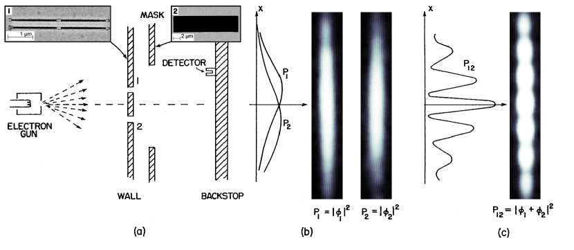
Feynman’s thought experiment is summarized in figure 1. The figure is an adaptation from Feynman Lectures on Physics, Volume III, figure 1-3, with the mask, experimental data, and micrographs added. The thought experiment contained two parts. The first involved observing probability distributions in three scenarios: electrons traveling through slit 1 with slit 2 closed (); electrons traveling through slit 2 with slit 1 closed (); and electrons traveling through both slits (). These scenarios illustrate the quantum mechanical superposition principle, i.e., the wave properties, and can be demonstrated with control of the slits (figure 2). The second part of the thought experiment was the observation of individual electrons associated with detection “clicks”. This illustrates that a quantum mechanical electron wave can not be thought of as comprising multiple electrons, i.e., the particle properties, which can be demonstrated with the build-up of the diffraction pattern (figure 3).
2 Experimental Setup
The experimental setup is shown diagrammatically in figure 1a. An electron beam with energy of 600 eV was generated with a thermionic tungsten filament and several electrostatic lenses. The beam was collimated with a slit of 2 m width and 10 m height placed at 16.5 cm. The double-slit was located 30.5 cm from the collimation slit. The resulting patterns were magnified by an electrostatic quadrupole lens and imaged on a two-dimensional microchannel plate and phosphorus screen, then recorded with a charge-coupled device camera.
Two methods were used to analyze the images. To investigate the probability distributions, the images were summed up by adding each frame’s intensity, then normalized. This resulted in a false colour probability distribution (figure 1 and 2). To study the build-up of the diffraction pattern, each electron was localized using a “blob” detection scheme[10, 11]. Each detection was replaced by a blob, whose size represents the error in the localization of the detection scheme. The blobs were compiled together to form the electron diffraction patterns (figure 3).
The collimation slit, double-slit, and mask were made by FIB milling into three 100-nm-thin silicon-nitride membrane windows. The FIB milling was performed on a 30-keV system (FEI Strata 200xp). After milling, each membrane was coated with approximately 2 nm of gold. The double-slit consists of two 50-nm-wide slits with a center-to-center separation of 280 nm (see inset 1 in figure 1). Each slit is 4 m tall and has a 150 nm support midway along it’s height. The mask is 5 m wide 10 m tall (see inset 2 in figure 1), and was placed 230 m away from the double-slit. The mask was held securely in a frame that could slide back and forth and was controlled by a piezoelectric actuator.
3 Results
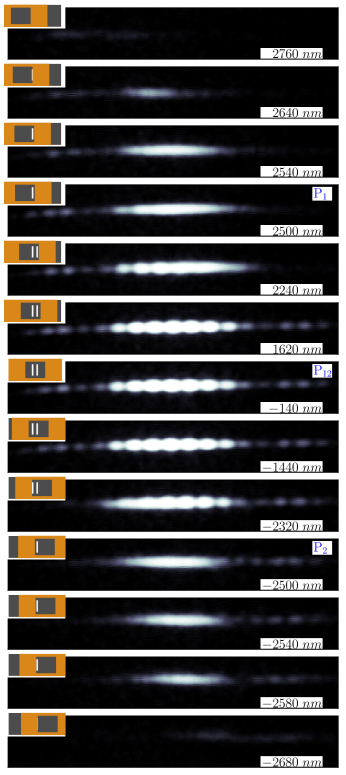
The movable mask was placed behind the double-slit, see figure 1. The mask was moved from one side to the other (figure 2 top to bottom). Initially the majority of the electrons are blocked. As the mask is moved, slit 1 becomes partially, then fully open. When one slit is open, single-slit diffraction can be observed ( in figure 2 and figure 1b). Feynman indicates this as the solid black curve (figure 1b), which is just the central order of the single-slit diffraction pattern. Because of the finite separation of the mask and double-slit, weak double-slit diffraction can be seen in the negative first order of the single-slit diffraction pattern (see left edge of in figure 2).
As the mask is moved further, more electrons can travel through both slits, changing the pattern from single-slit to double-slit diffraction. When the mask is centered on the double-slit, both slits are completely open and full double-slit diffraction can be observed ( in figure 2 and figure 1c). In this position, interaction between the mask and the diffracting electrons is negligible. The edges of the mask are 2500 nm away from the center and would only affect diffraction orders greater than the 60th. The mask is then moved further and the reverse happens; double-slit diffraction changes back to single-slit diffraction ( in figure 2 and figure 1b). Now, the single-slit diffraction pattern has a weak contribution of double-slit diffraction in its positive first order (see right edge of in figure 2). (See Supplementary Movie 1 for more positions of the mask.)
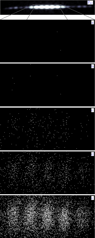
Electron build-up patterns were recorded with the mask centered on the double-slit. The electron source’s intensity was reduced so that the electron detection rate in the pattern was about 1 Hz. At this rate and kinetic energy, the average distance between consecutive electrons was meters. This ensures that only one electron is present in the 1 meter long system at any one time, thus eliminating electron-electron interactions. The electrostatic quadrupole lens was set to zoom in on the central five diffraction orders. In figure 3 the build-up of the diffraction pattern is shown. In figure 3a-c, the electron hits appear to be completely random and only after many electrons are accumulated can a pattern be discerned, figure 3d. In figure 3e the pattern is clearly visible. The final build-up of the pattern took about 2 hours. A full movie of the electron build-up is included in the supplementary data (see Supplementary Movie 2).
4 Conclusion
In this paper, we show a full realization of Feynman’s thought experiment and illustrate key features of quatum mechanics: interference and the wave-particle duality of matter. By controlling the transmission through the individual slits of a double-slit we were able to observe the diffraction patterns from slit 1 (), slit 2 (), and both (), thus observing the wave properties of electrons. Also, by recording single electron detection events diffracting through a double-slit we were able to build up a diffraction pattern, thus observing the particle properties of electrons.
References
References
- [1] Feynman R, Leighton R B and Sands M L 1965 The Feynman Lectures on Physics: Quantum Mechanics vol 3 (Reading: Addison-Wesley Pub. Co.) ch 1
- [2] Jönsson C 1961 Elektroneninterferenzen an mehreren künstlich hergestellten Feinspalten Z. Phys 161 454-74
- [3] Merli P G, Missiroli G F and Pozzi G 1976 On the statistical aspect of electron interference phenomena Am. J. Phy. 44 306-7
- [4] Tonomura A, Endo J, Matsuda T, Kawasaki T and Ezawa H 1989 Demonstration of single-electron buildup of an interference pattern Am. J. Phy. 57 117-20
- [5] Crease R P 2002 The most beatiful experiment Phys. World 15(9) 19-20
- [6] Crease R P 2002 The double-slit experiment Phys. World 15(9) 17 available at http://physicsworld.com/cws/article/print/9745
- [7] Barwick B, Gronniger G, Lu Y, Liou S Y and Batelaan H 2006 A measurement of electron-wall interaction using transmission diffraction from nanofabricated gratings J. Appl. Phys. 100 074322
- [8] Frabboni S, Gazzai G C and Pozzi G 2007 Young’s double-slit interference experiment with electrons Am. J. Phy. 75 1053-5
- [9] Frabboni S, Gazzai G C and Pozzi G 2008 Nanofabrication and the realization of Feynman’s two-slit experiment Appl. Phys. Lett 93 073108
- [10] Lindeberg T 1994 Scale-Space Theory in Computer Vision (Dordrecht: Kluwer Academic Publishers)
- [11] Lindeberg T 1998 Feature detection with automatic scale selection Int. J. Comput. Vision 30(2) 79-116