Enhanced Many-Electron Effects on Excited States of Gated Bilayer Graphene
Abstract
By employing the first-principles GW-Bethe-Salpeter Equation (BSE) simulation, we obtain, for the first time, the accurate quasiparticle (QP) band gap, optical absorption spectra and their dependence on the gate field of gated bilayer graphene (GBLG). Many-electron effects are shown to be extremely important to understand these excited-state properties; enhanced electron-electron interactions dramatically enlarge the QP band gap; infrared optical absorption spectra are dictated by bright bound excitons. Our results well explain recent experiments and satisfyingly solve the puzzle about the inconsistency between experimentally measured transport and optical band gaps. Moreover, our calculation reveals fine excitonic structures and predicts exotic excitonic effects that have not been observed yet, which can be of interest for optoelectronics applications based on GBLG.
pacs:
73.22.Pr, 78.67.Wj, 71.35.CcDespite its intriguing electronic, thermal and optical properties 2004MonoG ; 2007Graphene ; review-1 , intrinsic graphene is a gapless semimetal, impeding its utility in bipolar devices and subsequent broad applications. Therefore, huge efforts have been made to overcome this barrier by generating a finite band gap in graphene or its derivatives 2007BBG1 ; 2007BBG2 ; Graphane ; Fluorographene . One promising approach is to apply the gate electric field perpendicular to the AB (Bernal) stacked bilayer graphene (BLG) to break the inversion symmetry of sublattices 2007BBG1 ; 2007BBG2 ; 2007Transport1 ; 2009Optical1 ; 2009Optical2 . Such an induced band gap of GBLG can be tuned in a wide range by field strength 2009Optical1 ; 2007Transport1 ; 2010Transport2 ; 2012Transport3 , offering an important degree of freedom to optimize performance of graphene devices.
However, we are still in lack of a satisfying understanding on fundamental properties of GBLG, such as its quasiparticle (QP) band gap and optical excitations. For instance, electrical conductance experiments 2007Transport1 ; 2010Transport2 ; 2012Transport3 have confirmed the existence of a finite QP band gap but their measured value is annoyed by the inevitable contact resistance between electrodes and graphene sheet; while noncontacting optical measurements 2009Optical1 ; 2009Optical2 ; 2009kim have revealed a tunable band gap in GBLG but these results are indirect because the optical absorption peak (edge) is not conceptually equivalent to the QP band gap BSE ; review-BSE . Particularly, enhanced excitonic effects often dramatically shift the optical absorption peak as we have seen in many other reduced dimensional semiconductors Catalin2004 ; Feng2005 , making this inconsistence even more serious. Therefore, an accurate calculation with many-electron effects is urgent to settle the above inconsistency.
Conventional density functional theory (DFT) simulations cannot answer above questions because of their known deficiencies of handling excited-state properties BSE ; review-BSE ; GW . Tight-binding models TBGWBSE have revealed appealing physics of excitons in GBLG, but it has to rely on parameters. In particular, recent ab initio GW-BSE simulation has successfully predicted enhanced many-electron effects on intrinsic graphene BSEGraphene , which are confirmed by subsequent experiments graphene-1 ; graphene-2 ; graphene-3 . Therefore, a reliable first-principles calculation with many-electron effects included is also promising.
More importantly, beyond providing reliable parameters for device design, obtaining knowledge about excited states of GBLG will be of fundamental interest because it will fill our knowledge gap on many-electron interactions in two-dimension (2-D) narrow-gap semiconductors, a field that has not been well understood yet. In fact, it is challenging for first-principles simulations to accurately capture the nearly metallic electronic screening of narrow-gap semiconductors. For this purpose, an improved algorithm has to be developed and shall be of broad interest for the electronic-structure community.
In this Letter, with the modified model accurately describing the screening, we conclude three important remarks about excited states of GBLG. 1) The QP band gap and its dependence on the gate field are obtained. The self-energy correction is significant because of the enhanced electron-electron (e-e) interactions; the calculated QP band gaps are more than 150 % of previous DFT predictions LDA1 ; LDA2 , which is beneficial for device applications since a wider band gap implies higher working temperature. 2) Optical absorption spectra of GBLG are dominated by excitonic effects. With electron-hole (e-h) interactions included, our calculated absorption peaks are in excellent agreement with recent experiments 2009Optical1 , well explaining the inconsistency between QP gap and optical gap. 3) Excitons in GBLG exhibit a number of unusual features. For example, the electron and hole of the lowest-energy dark exciton are completely separated onto two graphene layers, giving rise to an optical approach to polarize BLG. Moreover, this separation of electron and hole offers a neat opportunity to evaluate entangling effects, such as the exchange interaction, of many-electron systems.
To reveal the significance of many-body correlations in GBLG, we perform the calculation of excited states as the following procedure. First, ground-state energy and wavefunctions are obtained by DFT within the local density approximation (LDA). Secondly, the QP energy is calculated within the single-shot approximation GW . Finally we obtain the exciton energy, wavefunctions and optical absorption spectra by solving the following BSE BSE
| (1) |
where is the amplitude of excitonic state consisting of single-particle hole state and electron state . is the e-h interaction kernel and is the exciton excitation energy. and are QP energy of electrons and holes, respectively.
All calculations are based on plane-wave basis and norm-conserving pseudopotential approximations with a 60-Ry energy cutoff. To eliminate the spurious interaction between neighboring BLG, the slab-truncation scheme is applied to mimic isolated GBLG Truncation1 ; Truncation2 . The electric field is applied by the periodic sawtooth potential perpendicular to graphene layers.
The crucial part of describing many-electron interactions is to obtain the dielectric function. For GBLG with the truncated Coulomb interaction, the inverse static dielectric function rapidly changes within the long wave-length regime , which is similar to what have been noticed in recent first-principles simulations of carbon nanotubes (CNTs) Catalin2004 . A brute-force way to capture this feature is to use a dense q-grid, which demands formidable computational resources. To solve this problem, we deliberately employ the mini Brillouin zone (BZ) sampling scheme to count in this sharply-varying character as motivated by Refs. Truncation1 ; Truncation2 , and extend it to both evaluating the QP energies and solving the BSE (see the supplementary material for details). As a result, a coarse k-grid sampling is adequate for the GW calculation. In addition, we employ a partial fine k-grid sampling around the Dirac cone for a dependable BSE calculation.
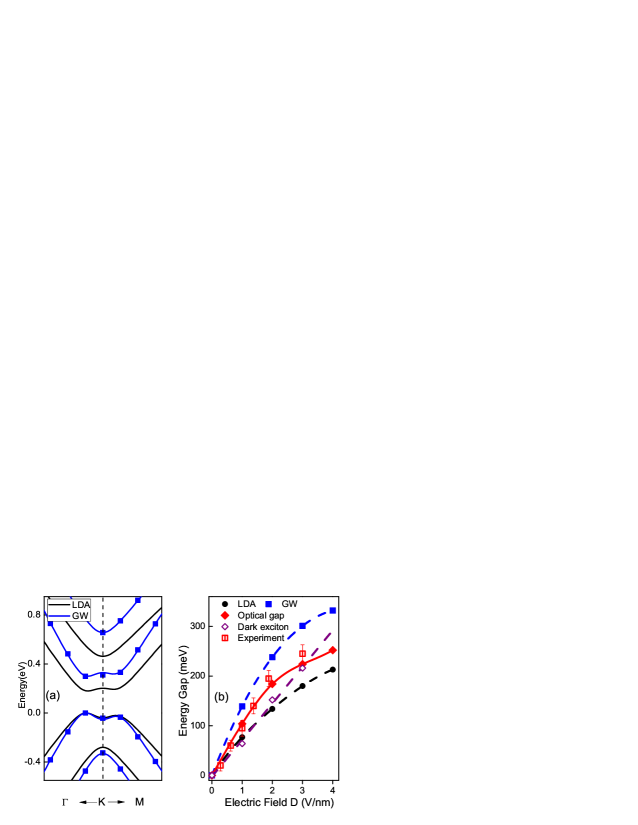
The LDA and band structures near the BZ corner (the K point) are plotted in Fig. 1 (a) for GBLG, respectively. The applied gate field induces a finite band gap and changes the band dispersion to the Mexican-hat feature. After including the self-energy correction via the GW calculation, the Mexican-hat-shaped feature remains intact, nevertheless the fundamental band gap is significantly enlarged due to the depressed screening of isolated GBLG. Moreover, the slope of band dispersion is sharpen by the self-energy correction, implying a smaller effective mass of free carriers.
We also investigate the QP band gap dependence on the applied gate field as shown in Fig. 1 (b). The QP band gap can be varied from zero up to 300 meV under experimentally reachable gate field, which is also more than 150 of previous DFT predictions. This larger tunable range and a wider gap are desired for device applications because a wider gap means higher working temperature and lower noise. Moreover, if listing the ratio of the self-energy correction to their DFT/LDA value, we see it is 56%, 67%, 78% and 81%, respectively, as the applied field is decreased. This growing trend of the correction ratio for the smaller gap is of particular interest because recent experiments 2012Transport3 shows a possible small band gap (around a few meV) even for BLG in the absence of gate field. However, due to the limit of the accuracy of our numerical simulation, we cannot resolve those energy differences below 10 meV and hence more advanced simulation technique needs to be developed.
In addition, the recent optical measurements of the optical gap are plotted in Fig. 1 (b) as well. The key feature is that the QP gap is substantially larger than both previous DFT predictions LDA1 ; LDA2 and measurements from optical experiments, SCFTB ; 2009Optical1 . The inconsistency QP band gap with optical measurements has also been observed in several other semiconducting nanostructures Catalin2004 ; Feng2005 , which manifests enhanced excitonic effects and motivates the following calculation on optical spectra of GBLG.
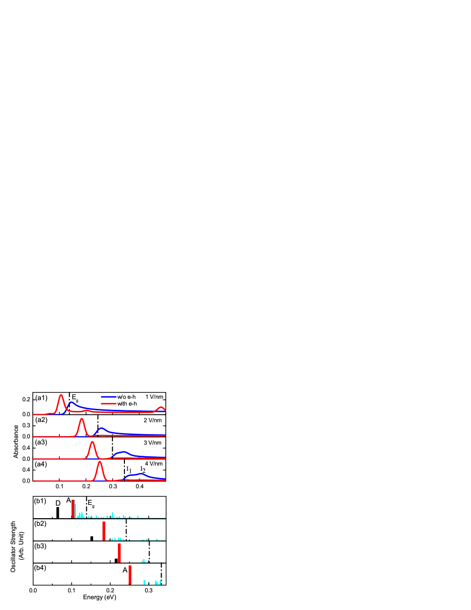
Fig. 2 depicts the optical absorption spectrum and its evolution subject to the increasing field magnitude. We first focus on absorption spectra in the absence of the e-h interactions (blue lines in Figs. 2 (a)). In the low-energy regime, the absorption is mostly contributed by the transition from the highest valence band (v1) and the lowest conduction band (c1). As expected, the absorption onset displays a blueshift as the electric field uplifts the band gap magnitude. Meanwhile, the prominent absorption feature is gradually broadened and split into a double-peak structure ( and ) which stems from the two one-dimensional-like von-Hove singularities TBGWBSE ; MultiLayer at opposite “Mexican-hat brims”(Fig. 1 (a)), which is consistent with previous DFT results LDA1 .
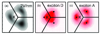
Surprisingly, the von-Hove singularity at the K point, however, does not contribute greatly to the absorption and therefore is not resolved in the spectra. This is because the relevant valence state and the conduction state at the Dirac point K are strongly localized on different layers upon field-induced symmetry breaking. Therefore, the overlap of wavefunctions is very small, which eventually leads to a negligible oscillator strength. This can be seen in Fig. 3 (a), in which we present the contour plot of the oscillator strength around the corner of the first BZ. The strongest oscillator strength is actually from the “Mexican-hat brims”regime while it is almost zero at the K point.
With e-h interactions included, a different optical absorption picture emerges. As shown in Figs. 2 (a), the exciton effect dramatically reshapes the spectra; the broad asymmetric absorption peak in the single-particle picture is replaced by a symmetric prominent absorption peak. This peak lies below the QP band gap, indicating the existence of bound e-h pairs. The binding energy under four sampling voltages is 35, 54, 76 and 80 meV, respectively, which is also close to previous tight-binding calculations TBGWBSE . Remarkably these peak-position is in excellent agreement with the previous infrared microspectroscopy experiment 2009Optical1 as shown in Fig. 1 (b). Under realistic experimental setups, both self-energy corrections and e-h interactions shall be reduced by the screening effect of dielectric substrates. On the other hand, these reductions may cancel each other more or less 2011yang , resulting in such a good match of our calculations with experimental data.
In the higher energy regime (around 0.4 eV) next to the first optical active peak, the absorbance maintains a constant on the whole ( 3), which is significantly smaller than 4.6%, the ideal value of the optical absorbance of BLG optical-2 ; BGConstant2 . This is due to the sum rule of oscillator strength BSE because e-h interactions drains the absorbance from the high-energy regime to enhance the exciton peak.
It has to be pointed out that electron-phonon coupling shall be another important factor in determining the infrared optical spectra of GBLG. For example, a G-mode phonon at 195meV has been found to be in Fano interference coupled with e-h excitations in GBLG 2010wang . Therefore, we may expect this dip feature from such a G-mode phonon may impact the lineshape of our studied exciton absorption peaks.
A close inspection of solutions of the BSE reveals an intriguing exciton picture that have not been observed by experiments. We plot the oscillator strength of excitons in a logarithmic scale in Figs. 2 (b). The isolated exciton state with the largest oscillator strength, , is responsible for the symmetric prominent absorption peaks in the spectra. Surprisingly, there is one lower-lying excion, , with a much weaker oscillator strength for most gated fields (except 4V/nm). This is contrary to the usual effective-mass model, in which the lowest singlet exciton shall be the brightest one involved with two bands.
Furthermore, we observe that both the position and oscillator strength of this dark exciton are more sensitive to the gate field than those of bright exciton . As plotted in Figs. 2 (b), the energy of progressively approaches that of with an increasing gate field strength and its optical activity is strongly quenched simultaneously. In particular, when the gate field is more than 3V/nm, the order of the bright and dark excitons is switched as shown in Fig. 1 (b). This tunable energy difference can surely affect the thermal population of exciton states and their luminescent performance. Such a tunable energy order of excitons is in qualitative agreement with previous tight-binding studies TBGWBSE .
To understand the brightness of these exciton states, we need to further investigate the origin of their optical activity. For a typical field strength (2 V/nm), Figs. 3 (b) and (c) display the distribution of the square of exciton amplitude for those two interested excitons and . Since the optical activity of an exciton BSE is
| (2) |
which roughly means the product of the single-particle oscillator strength shown in Fig. 3 (a) and exciton amplitude shown in Figs. 3 (b) or (c), we immediately see the product of exciton is much bigger than exciton , suggesting their markedly different brightness.
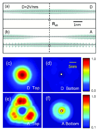
Fig. 4 visualizes exciton wavefunctions in the real space. As is readily seen, both excitons and are strong charge transfer excitons but with distinct characters. In particular, the electron and hole of the dark exciton almost become disentangled. As shown in Figs. 4 (a), (c) and (d), the electron and hole wavefunctions of exciton are nearly completely separated into two layer. This is very dissimilar to the e-h correlation in other 2-D semiconductors GraphaneXcton ; BSEGraphene . From the perspective of optoelectronic application, exciton could yield interesting possibility of efficient e-h separation and polarize BLG by optical excitations. For the exciton , the degree of e-h separation is much lower. In Figs. 4 (b), (e) and (f), the electron distributes over a ring on the top layer while on the bottom layer the electron distributes on a disk centered at the hole.
Moreover, these excitonic wavefunctions will be crucial to understand why the dark exciton and the dark exciton respond very differently to the electric field. As concluded in Fig. 1 (b), the energy level of exciton exhibits an approximately linear relationship with the field strength, whereas that of exciton shows a nonlinear behavior. This can be rationalized by the fact that exciton can be viewed as a plane of dipole composed of dissociated electron and hole as revealed in Fig .4 (a), whose energy levels of the positive and negative poles linearly depend on the applied gate field. In contrast, the electron and hole for the exciton are spatially entangled and therefore the energy level is less sensitive to the gate field and does not follow a simple linear trend. This explains the origin of the energy order switch when the applied gate field is more than 3 V/nm.
In conclusion, we have provided first-principles calculations for the QP energy and excitonic effects of GBLG. E-e and e-h interactions are significant and must be considered to understand the electronic structure and optical excitations of GBLG. Moreover, our calculation well explains recent experiments and reveals more physics associated with many-electron effects. Finally, we have observed an exotic dark exciton structure that is not likely to present in conventional direct band gap semiconductors. The different degree of charge transfer for different exciton states may be useful in optoelectronic applications.
The computational resources have been provided by Lonestar of Teragrid at the Texas Advanced Computing Center. The ground state calculation is performed by the Quantum Espresso. The GW-BSE calculation is done with the BerkeleyGW package BGW with minor modifications for excited states calculations in GBLG.
References
- (1) K.S. Novoselov et al., Science 306, 666 (2004).
- (2) A. K. Geim and K. S. Novoselov, Nature Materials 6, 183-191 (2007).
- (3) A. H. Castro Neto, et al, Rev. Mod. Phys. 81, 109 (2009).
- (4) J. O. Sofo, A. S. Chaudhari, and G. D. Barber, Phys. Rev. B 75, 153401 (2007).
- (5) J. T. Robinson et al, Nano Lett. 10, 3001-3005 (2010).
- (6) E. V. Castro et al., Phys. Rev. Lett. 99, 216802(2007).
- (7) T. Ohta et al., Science 313, 951(2006).
- (8) K. F. Mak, C. H. Lui, J. Shan, and T.F. Heinz, Phys. Rev. Lett. 102 256405 (2009).
- (9) Y. Zhang et al., Nature 459 820-823(2009).
- (10) J. Yan, T. Villarson, E.A. Henriksen, P. Kim, and A. Pinczuk, Phys. Rev. B 80 241417 (2009).
- (11) J.B. Oostinga et al., Nature Material 7, 151-157 (2007).
- (12) T. Taychatanapat and P.J. Herrero, Phys. Rev. Lett. 105, 166601 (2010).
- (13) J. Velasco Jr et al., Nature Nanotechnology 7, 156-160 (2012).
- (14) M. Rohfling and S.G. Louie, Phys. Rev. B 62, 4927 (2000).
- (15) G. Onida, L. Reining, and A. Rubio, Rev. Mod. Phys. 74, 601 (2002).
- (16) C.D. Spataru, S. Ismail-Beigi, L.X. Benedict, and S.G. Louie, Phys. Rev. Lett. 92, 077402 (2004).
- (17) F. Wang et al, Science 308, 838 (2005).
- (18) M.S. Hybertsen and S.G. Louie, Phys. Rev. B 34, 5390 (1986).
- (19) C.H. Park and S.G. Louie, Nano Lett. 10, 426-431 (2010).
- (20) L. Yang et al., Phys. Rev. Lett. 103, 186802 (2009).
- (21) V.G. Kravets, et al, Phys. Rev. B 81, 155413 (2010).
- (22) K.F. Mak, J. Shan, and T.F. Heinz, Phys. Rev. Lett. 106, 046401 (2011).
- (23) D.-H. Chae, et al, Nano Lett. 11, 1379 (2011).
- (24) H. Min, B. Sahu, S. K. Banerjee, and A.H MacDonald, Phys. Rev. B 75. 155115 (2007).
- (25) L. Yang, Phys. Rev. B 81, 155445 (2010).
- (26) S. Ismail-Beigi, Phys. Rev. B 73, 233103 (2006).
- (27) C.A. Rozzi et al., Phys. Rev. B 73, 205119 (2006).
- (28) L.M. Zhang et al., Phys. Rev. B 78, 235408 (2008).
- (29) C.L. Lu et al., Phys. Rev. B, 73, 144427 (2006).
- (30) L. Yang, Nano Lett. 11, 3844 (2011).
- (31) T.-T. Tang et al., Nature Nanotech. 5, 32 (2010).
- (32) K.F. Mak et al., Phys. Rev. Lett. 101, 196405(2008).
- (33) R. R. Nair et al, Science 320, 1308 (2008).
- (34) P. Cudazzo, C. Attaccalite, I.V. Tokatly, and A. Rubio, Phys. Rev. Lett. 104, 226804(2010).
- (35) J. Deslippe et al, Computer Physics Communications, vol. 183, issue 6, 1269-1289 (2012).