Local and Tunable Geometric Phase of Dirac Fermions in a Topological Junction
Abstract
We discover a new type of geometric phase of Dirac fermions in solids, which is an electronic analogue of the Pancharatnam phase of polarized light. The geometric phase occurs in a local and nonadiabatic scattering event of Dirac fermions at a junction, unveiling topological aspects of scattering of chiral particles, and it is experimentally tunable to an arbitrary value. It provides a unique approach of detecting the topological order of the insulator in a metal-insulator junction of Dirac fermions, establishing new bulk-edge correspondence. The geometric phase also modifies the fundamental quantization rule of Dirac fermions, suggesting topological devices with nontrivial charge and spin transport such as a topological wave guide and a topological transistor.
pacs:
03.65.Vf, 73.25.+i, 73.20.-r, 72.80.VpPolarized light acquires geometric phase, when it passes through a series of polarizers Pancharatnam . This phase, known as Pancharatnam phase Pancharatnam ; Berry_Pan ; Bhandari ; Ben-Aryeh , is a topological phenomenon of geometric origin in Poincare sphere, a graphical tool representing light polarization on its surface; see Fig. 1. In academic viewpoints, this phase is essential for generalizing quantum geometric phase, known as Berry phase Berry ; Anandan , from an adiabatic cyclic evolution of quantum states to discontinuous or noncyclic changes Berry_Pan ; Bhandari ; Aharonov such as projective measurement. It has attracted much attention in optics, and used in various optical devices Bhandari .
Electron spin is a quantum counterpart of light polarization. It is also represented by Poincare (Bloch) sphere, suggesting new topological quantum effects in solids by Pancharatnam phase. However, Pancharatnam phase has not been considered in solids.
On the other hand, electrons in graphenes Neto and a surface of topological insulators Hasan ; Moore ; Qi behave as Dirac fermions (DFs). They are chiral particles with spin-momentum locking; in graphene, the pseudospin representing sublattice states replaces the spin. Because of the chiral spin-momentum locking, they acquire geometric phase in spatial motion, causing topological phenomena Novoselov ; Zhang ; Wilczek ; Falko ; Beenakker such as the half-integer quantum Hall effect, weak antilocalization, and Majorana fermions. Together with unusual transport of DFs Beenakker ; Katsnelson ; Park ; Park2 ; Cheianov , the control of the geometric phase will lead to topological electronics. However, the geometric phase germane to the known topological phenomena is nonlocal and not experimentally tunable; the phase has the fixed value of .
In this paper, we will theoretically demonstrate that because of the chiral behavior, a local and nonadiabatic scattering event of DFs at a junction surprisingly has geometric nature, resulting in Pancharatnam phase. The Pancharatnam phase of DFs can be tuned to an arbitrary value, by experimentally controlling the junction. Hence, the junction provides a platform for studying Pancharatnam phase, similarly to optical polarizers, but exhibits new roles of Pancharatnam phase in solids. The Pancharatnam phase establishes new bulk-edge correspondence for a metal-insulator junction, as it detects the topological order of the insulator side of the junction; the conventional correspondence states gapless edge states along the junction interface of two insulators with different topological order. The Pancharatnam phase also modifies the fundamental quantization rule of DFs. These findings suggest topological electronic devices with nontrivial charge and spin transport such as a topological wave guide and a topological field effect transistor.
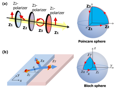
Pancharatnam phase of Dirac fermions.— For illustration, we consider DFs in a 2D step junction ( plane) in Fig. 1(b), governed by Hamiltonian , where for and for . They have Fermi velocity , charge , and the locking of momentum and Pauli spin operators . In experiments, the electrostatic potential is tuned by gates, and the energy gap is created in topological insulators by magnetic doping Chen or a ferromagnetic insulator Tanaka .
Pancharatnam phase equals the Berry phase along a geodesic polygon on the parameter space Berry_Pan , , where is the solid angle of . We find that appears in the scattering of an incoming plane wave at the step junction. In Fig. 1(b), is reflected to state or transmitted to . has spin , and satisfies the wave continuity at the interface , equivalently , with reflection (transmission) coefficient (). By using ( being the spin state orthogonal to ), we obtain the reflection phase Supple as
| (1) |
where denotes the inner product of spin states. In addition to the shift by reflection and the gauge dependent term of , has the Pancharatnam phase , whose geodesic polygon connects , , on Bloch sphere and has solid angle . Similarly, another Pancharatnam phase contributes to the transmission phase as
| (2) |
The relations (1) and (2) reveal the fundamental property that the scattering, a noncyclic and discontinuous process “projectively measuring” spin, has geometric nature. is gauge invariant, hence, physically observable. For example, one observes by measuring , with tuning but keeping unchanged. provides intuitive graphical understanding of . Contrary to usual geometric phases in solids, is acquired by propagating particles and experimentally tunable to arbitrary values . As shown below, has wide significance in solids.
Bulk-edge correspondence by Pancharatnam phase.— As the first significance, Pancharatnam phase provides a fundamental tool of detecting the Chern number Qi2 that characterizes the topological order of a DF insulator. To see this, we consider a metal-insulator step junction with and . Here, , propagating from metal to insulator with incidence angle , is reflected to via an evanescent state of the insulator; its energy is inside the gap , and at normal incidence. Then, appears in ; replaces in Eq. (1) and Fig. 1. We will show that the Chern number of the insulator is identified by .
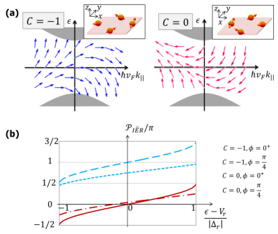
Figure 2(a) shows our finding that the spin of depends on . For any , the component of aligns parallel (antiparallel) to the junction interface, when (). Namely, represents the winding number of along insulator edges. This property is recognized by . For example, for , being positive (negative) infinitesimal, we find Supple that covers different domains for different [see Fig. 2(b)],
| (3) |
The sign factor results from the intrinsic property Bhandari2 of that jumps by Berry phase at . For , also recognizes via another inequality Supple .
Inequality (3) is independent of junction details of , , and . It establishes bulk-edge correspondence for a metal-insulator junction: , geometric phase by the scattering at the junction interface, recognizes , another geometric phase characterizing the topology of the energy band of the bulk insulator. This is in marked contrast to the conventional bulk-edge correspondence Qi2 about the existence of gapless metallic edge states in insulator-insulator junctions. Our new correspondence leads to (hence is more fundamental than) the conventional correspondence, as shown below.
Geometric contribution to quantization.— Next, we discuss another significance that modifies the fundamental quantization rule. For example, Eq. (1) indicates the Bohr-Sommerfeld semiclassical rule for a closed trajectory with length and ,
| (4) |
which has dynamical phase and shift at each of reflections in the trajectory. is the new contribution from the geodesic polygon connecting the states (propagating or evanescent ) involved along the trajectory in sequential order Supple . For the bound state in Fig. 3(a), we find . can be detected by observing bound states with tuning ’s, or from its unusual implications on interference, resonance, and quantum transport.
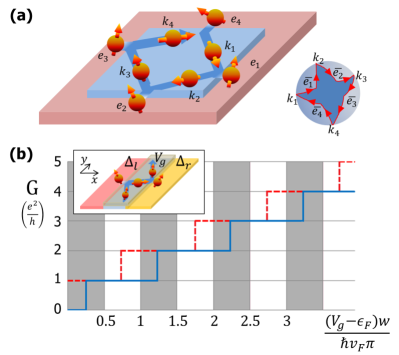
We focus on a topological waveguide with width between two insulators in Fig. 3(b). Its quantization rule is determined by ,
| (5) |
where . occurs in the reflection from the state of momentum in waveguide to the state of momentum via an evanescent state of insulator , while from to via an evanescent state of insulator . Contrary to usual non-topological cases without , the quantization rule in Eq. (5) depends on . Electron conductance along the waveguide jumps by as varies, whenever an additional channel satisfies Eq. (5).
When , Eq. (5) becomes , namely, . Its solution exists when , describing edge states in the interface between the insulators and . However, it never exists when ; one can see this by analyzing . Hence, our bulk-edge correspondence based on leads to the conventional version Qi2 based on edge states.
The waveguide with finite shows another topological feature of in Fig. 3(b). When its Fermi energy satisfies , the jumps of by occur within the domains of that have no overlap between the cases of and . The jumps occur within the domains of for , while for ; . The origin is that the winding direction of is opposite between the two cases Supple . Hence, the two topologically different cases of and are distinguished by the conductance jumps. This feature is useful for experimentally observing .
Geometric-phase device.— Finally, the above features of suggest geometric-phase devices with new functionality. In Fig. 4, we consider a Fabry-Pérot resonator; it has the same setup as the waveguide, but is located above the gaps . The transmission probability of a plane wave through the resonator is well known, but modified by the quantization rule in Eq. (5) as
| (6) |
where () are the reflection (transmission) probability at the interface between regions and , and now means the propagating state of region . Note that Fabry-Pérot resonators of DFs have been studied in different contexts from in literature Katsnelson ; Park ; Yokoyama .
Figure 4(b) shows for a plane wave with energy incoming from the left metallic region with incidence angle or from the right region with . A resonance occurs in when . Namely, the plane wave can pass through the resonator only at certain resonance angles of , which is controllable by . Interestingly, because of , the occurrence of the resonance is (more) asymmetric, with respect to for (larger) . And , causing the possibility that when a state from the left region resonantly passes through the resonator to in the right , the time-reversed state of in cannot pass to . It is because the two processes are affected by different . These features do not occur in the systems of nonchiral electrons.
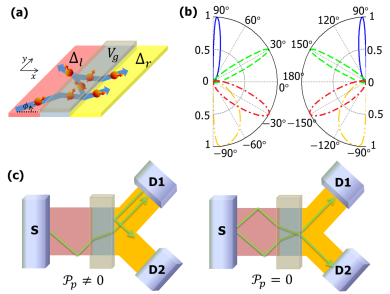
The above features suggest a multi-terminal device in Fig. 4(c). Here, by tuning , one switches on and off charge and spin current in D1 and D2 simultaneously when (since ), or separately when . The switching will be efficient, as one achieves the collimation of charge propagation and spin direction by a narrow resonance of under certain parameters. Since , this device also behaves as a spin diode where spin current from S to D1 or D2 (from D1 or D2 to S) is switched on (off); see the left panel of Fig. 4(c). It may be used as a logic gate of spin.
Conclusion.— We remark that Pancharatnam phase will be ubiquitously found in various DF systems, including 1D zigzag edges of graphene, non-planar 2D surfaces Seo ; Dahlhaus , 3D matters Hasan ; Moore ; Qi , and interferometers such as an electronic Veselago lens Park ; Park2 ; Cheianov . For example, a plane wave of DFs acquires Pancharatnam phase in a scattering event by a zigzag edge, while it does not by an armchair edge Choi . will also appear in bilayer graphene of massive DFs, and in photonic Wang or sonic Torrent crystals of bosonic chiral particles. The case of bilayer graphene is of special interest, as is tuned by electrostatic gates Ohta .
We emphasize that will open a unique way to topological electronics, as it is acquired by propagating particles, experimentally tunable, and immune to dephasing (since it occurs in a local nonadiabatic event).
We thank A. H. MacDonald and J. E. Moore for discussions, UC Berkeley, where part of this paper was written, for hospitality, and the support by Korea NRF grant (2011-0022955).
References
- (1) S. Pancharatnam, Proc. Indian Acad. Sci. A44, 247 (1956).
- (2) M. V. Berry, J. Mod. Opt. 34, 1401 (1987).
- (3) R. Bhandari, Phys. Rep. 281, 1 (1997).
- (4) Y. Ben-Aryeh, J. Opt. B:Quantum Semiclass. Opt. 6 R1 (2004).
- (5) M. V. Berry, Proc. R. Soc. A392, 45 (1984).
- (6) J. Anandan, Nature 360, 307 (1992).
- (7) Y. Aharonov and J. Anandan, Phys. Rev. Lett. 58, 1593 (1987).
- (8) A. H. Castro Neto, F. Guinea, N. M. R. Peres, K. S. Novoselov, and A. K. Geim, Rev. Mod. Phys. 81, 109 (2009).
- (9) M. Z. Hasan and C. L. Kane, Rev. Mod. Phys. 82, 3045 (2010).
- (10) J. E. Moore, Nature 464, 194 (2010).
- (11) X.-L. Qi and S.-C. Zhang, Rev. Mod. Phys. 83, 1057 (2011).
- (12) K. S. Novoselov et al., Nature 438, 197 (2005).
- (13) Y. Zhang, Y.-W. Tan, H. L. Stormer, and P. Kim, Nature 438, 201 (2005).
- (14) F. Wilczek, Nat. Phys. 5, 614 (2009).
- (15) V. I. Fal’ko et al., Solid State Commun. 143, 33 (2007).
- (16) C. W. J. Beenakker, Rev. Mod. Phys. 80, 1337 (2008).
- (17) M. I. Katsnelson, K. S. Novoselov, and A. K. Geim, Nat. Phys. 2, 620 (2006).
- (18) S. Park and H.-S. Sim, Phys. Rev. Lett. 103, 196802 (2009).
- (19) S. Park and H.-S. Sim, Phys. Rev. B 84, 235432 (2011).
- (20) V. V. Cheianov, V. Fal’ko, and B. L. Altshuler, Science 315, 1252 (2007).
- (21) Y. Chen et al., Science 329, 659 (2010).
- (22) Y. Tanaka, T. Yokoyama, and N. Nagaosa, Phys. Rev. Lett. 103, 107002 (2009).
- (23) X.-L. Qi, Y.-S. Wu, and S.-C. Zhang, Phys. Rev. B 74, 045125 (2006).
- (24) R. Bhandari, Phys. Lett. A 157 221 (1991).
- (25) T. Yokoyama, Y. Tanaka, N. Nagaosa, Phys. Rev. Lett. 102, 166801 (2009).
- (26) J. Seo et al., Nature 466, 343 (2010).
- (27) J. P. Dahlhaus, C.-Y. Hou, A. R. Akhmerov, and C. W. J. Beenakker, Phys. Rev. B 82, 085312 (2010).
- (28) T. Ohta, A. Bostwick, T. Seyller, K. Horn, and E. Rotenberg, Science 313, 951 (2006).
- (29) Z. Wang, Y. Chong, J. D. Joannopoulos, and M. Soljaić, Nature 461, 772 (2009).
- (30) D. Torrent and J. Sánchez-Dehesa, Phys. Rev. Lett. 108, 174301 (2012).
- (31) S.-J. Choi, S. Park, and H.-S. Sim, in preparation.
- (32) See the supplementary information for the details.