Quantum phase slips in superconducting Nb nanowire networks deposited on self-assembled Si templates
Abstract
Robust porous silicon substrates were employed for generating interconnected networks of superconducting ultrathin Nb nanowires. Scanning electron microscopy analysis was performed to investigate the morphology of the samples, which constitute of polycrystalline single wires with grain size of about 10 nm. The samples exhibit nonzero resistance over a broad temperature range below the critical temperature, fingerprint of phase slippage processes. The transport data are satisfactory reproduced by models describing both thermal and quantum fluctuations of the superconducting order parameter in thin homogeneous superconducting wires.
pacs:
74.78.Na, 73.63.NmThe research activity in the field of superconductivity at reduced dimension has been continuously growing AruPhysRep ; BezTopRev , due to the major implications that these results can have for understanding fundamental phenomena Johansson ; Lau as well as for possible applications in superconducting electronics Astafiev ; Ku ; Nazarov ; BezrPRB ; BezNNW . The behavior of the so-called superconducting nanowires, namely ultrathin samples with dimensions comparable with the superconducting coherence length, , is dominated by both thermal activated phase slips (TAPS) and quantum phase slips (QPS) processes Giordano , causing the wires to remain resistive much below the superconducting transition temperature. The most challenging aspect of the experimental study of nanowires is the difficulty of fabricating homogeneous samples, since it has been widely demonstrated that sample inhomogeneity can be the source of broadened superconducting transitions Bollinger ; Zgirsti ; Patel . From the early studies realized on crystalline superconducting whiskers Tinkham , advances in nanofabrication techniques have allowed the realization of high quality single crystals nanowires Wang . Even more sophisticated is the approach of using suspended carbon nanotubes or DNA molecules as templates for the formation of superconducting nanowires BezryadinNature ; BezryadinScience ; BezryadinAM . A radically different approach to nanostructures fabrication based on self-assembled growth attracted much attention also in the superconducting nanowire field Yi ; Michotte ; Tian ; Kwok . Most of these works rely on the deposition within the channels and cavities of porous membranes. Self-assembled methods are versatile and reliable bottom-up techniques for generating low-cost patterns of nanostructures, assuring a highly reproducible geometry on very large areas.
In this work the formation of interconnected networks consisting of Nb ultrathin superconducting nanowires is achieved by using Porous Silicon
(PS) as template substrate. The extremely reduced film thickness favors the deposited material to occupy only the substrate pitch, therefore the
as-sputtered films result as a network of interconnected wires, whose average width, , can be assumed to be equal to the periodic pore spacing
minus the pore diameter. Due to the extremely reduced characteristic dimension of the substrate is comparable to the superconducting coherence
length , and hence each individual wire behaves as a one-dimensional (1D) object. As a consequence, the whole samples show broadened
resistive transitions, which can be described by theoretical models for both thermal and quantum fluctuations of the order parameter in 1D
superconductors Zaikin1 ; Zaikin2 ; Bae . The proposed technique allows one to overcome the problem of handling fragile membranes usually used
at this purpose Yi ; Michotte ; Kwok employing robust PS crystals as stable support. Moreover, the analyzed systems are rather simple and
macroscopically large objects, which, however, reveal fascinating quantum effects. Finally, compared to similar self-assembled nanowire networks
Kwok exhibiting thermal phase slippage, the system presented in this work provides strong evidence of QPS.
PS was fabricated by
electrochemical anodic etching of n-type, 0.01 cm, monocrystalline Silicon wafers as previously described in Refs. Trezza1 ; Trezza2 .
The resulting porous substrates, covering an area of about 2 cm2, have average pore diameter nm and average interpore spacing
(defined as the distance between the centers of two consecutive pores) nm. Nb ultrathin films were deposited on top of PS substrates
in an UHV dc diode magnetron sputtering system with a base pressure in the low 10-8 mbar regime following the same fabrication procedure
described elsewhere Trezza1 ; Trezza2 . Since the effect of the periodic template is reduced when the film thickness, , exceeds the
pore diameter Trezza1 , the thickest Nb films deposited for transport measurements have nm. With this approach an array of
interconnected Nb wires is guided by the PS template, the single wire width being the substrate pitch ( nm). Finally, the samples
were patterned by standard optical lithography and lift-off procedure into bridges of width m and length m,
to obtain a classical pseudo-4-point geometry (meaning two contacts, each used for a current and a voltage lead). The effect of the patterning is
to reduce the number of interconnected wires under study.
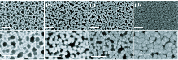
Fig. 1 shows high resolution images of the surface of superconductive nanowire networks obtained from a template with
nm and nm, performed by Field Emission Scanning Electron Microscopy (FESEM) (igma Gemini by Zeiss). The images of four different
samples are reported in the panels: (a) S0, a free nanoporous Si substate, (b, c, d) three Nb films (S3.5, S7, and S15) with nominal thicknesses
, and 15 nm, respectively. The images were acquired at two different magnifications (600 Kx and 1312 Kx) and clearly show the
evolution of the morphology with the progressive Nb deposition. It emerges that the single nanowires are polycrystalline with well shaped grains
with increasing dimension of 10 - 20 nm for increasing values. Images have been analyzed by SPIP SPIP , a software for image
analysis, in order to evaluate the average diameter of pores, , and grain size, . These value are summarized in Table 1.
From the FESEM analyses, it follows that the optimal Nb thickness to investigate the superconducting properties of the nanowire array should lie in the range nm. This, in fact, assures that the wires are continuous, while preserving the presence of a well defined network. Moreover, at these reduced thicknesses the system could approach the 1D limit. The characteristic parameters of these samples are listed in Table 2.
| sample | (nm) | (nm) | (nm) |
|---|---|---|---|
| S0 | 0 | - | 15 |
| S3.5 | 3.5 | 10 | 13 |
| S7 | 7 | 11 | 11 |
| S15 | 15 | 20 | 6 |
Superconducting transition temperatures, , and critical currents, , were resistively measured in a 4He cryostat using a standard dc four-probe technique. Transport measurements provide also a probe of the quality and the homogeneity of the nanowires. It is worth underlining that on the same kind of unstructured samples an extensive electrical characterization was performed, which revealed that ultrathin Nb films deposited on PS substrates exhibit well established superconducting properties Trezza1 ; Trezza2 comparable with the ones of conventional plane films. It has been also demonstrated that the size and spacing of PS pores is well matched to the vortex lattice of Nb thin films, giving rise to matching effects at high magnetic fields and low temperature Trezza1 ; Trezza2 . The standard lift-off processing on a micrometer scale is not expected to induce drastic sample imperfections which could be responsible of a dramatic resistance versus temperature, , broadening. Resistivity of the single wires is difficult to estimate accurately due to the particular nanowires arrangements. However, on first conservative approximation, it is reasonable to assume for a value comparable with the one obtained for plane Nb ultrathin films Lehtinen , which for sample deposited in the same sputtering system under the same conditions varies between and 35 cm for thickness in the analyzed range rho . Knowing the material constant l for Niobium Minhaj , namely 10-6 cm2, it results that the value of the low temperature mean free path is l 1 nm in agreement with the values reported for ultrathin Nb nanowires BezAPL . Moreover, being l , it follows that the samples are in the dirty limit, an important requirement for the occurrence of QPS processes, since the probability of a QPS event can be expressed as (here is the wire cross sectional area) indicating that low temperature superconductors with high resistivity are the best candidates for observing QPS. Compared to MoGe-based nanowire network Kwok the detection of QPS is favored for Nb wires, since the required condition AruPhysRep , where is the temperature dependent superconducting gap, is realized at higher temperatures. Fig. 2 shows the resistive transitions for all the analyzed samples. Measurements were performed using a constant bias current A. The first step in the curves is due to the transition of the electrodes AruPhysRep ; BezryadinNature , therefore the values of , reported in Table 2, were evaluated at the midpoint of the transition occurring below the first one. Correspondingly, the normal state resistance, , is defined as the sample resistance below the electrodes transition AruPhysRep ; BezryadinNature . The main feature of the curves is the nonzero resistance over a wide temperature range, which is strongly reminding of a 1D behavior. It also deserves noticing that the curves do not show any steps or humps, which can be a signature of inhomogeneity Bollinger . Moreover, the moderate values of the normal state resistance (, where is the quantum resistance k) exclude that weak links constrictions or the film granularity can be responsible of the conduction Bollinger . In order to further demonstrate the good quality of the samples and to exclude the presence of tunneling barriers at the grain boundaries, it is useful to analyze both the shape of the voltage-current () characteristics and the values of their critical current density, BezryadinNature . Indeed at low temperature the shape of the characteristics (not shown here) are very sharp and present no steps or hysteresis. The values of are comparable with the ones measured on Nb perforated thin films JAPCara . The critical current of the network is, indeed, , where is the critical current of the single wire, which is related to its depairing current, , via .Zant It follows that from the measured values, the depairing current density of the single nanowire at can be estimated to be 1010 A/m2, about one order of magnitude smaller than the depairing current density evaluated in the framework of the model by Kupriyanov and Lukichev KL (KL) 1011 A/m2, a discrepancy comparable to the one reported in the case of Nb perforated thin films JAPCara . Moreover, in the present case, this difference may be attributed, for instance, to the approximation performed calculating the values of , namely to the complex morphology of the samples.
| sample | (nm) | (nm) | (nm) | (nm) | (m) | (K) | |
|---|---|---|---|---|---|---|---|
| S9 | 20 | 10 | 9 | 9.5 | 500 | 10 | 3.39 |
| S10 | 40 | 30 | 10 | 17.3 | 250 | 10 | 3.52 |
| S12 | 40 | 30 | 12 | 19.0 | 500 | 20 | 3.57 |
Having clarified the issue of the sample homogeneity, it is possible to analyze the curves in the framework of the theoretical models proposed for 1D superconductors to describe both thermal and quantum phase slip processes. Indeed the systems under study consist of interconnected networks of ultrathin Nb nanowires with width ( nm) comparable to the Nb superconducting coherence length. The latter was estimated from the temperature dependence of the perpendicular upper critical field, , obtained performing resistance versus field, , measurements at fixed values of the temperature. Indeed it follows that the Ginzburg-Landau coherence length at zero temperature is nm. In presence of thermal activated phase slip processes the resistance is described by the equation Zaikin2 :
| (1) |
| (2) |
where is a crossover temperature between TAPS and QPS regime, is the nanowire length, and and are the temperature dependent coherence length and phase slip activation energy, respectively. Since is not well defined in these samples Kwok , it is treated as fitting parameter together with and, in the case of Eq. 1 (2), the parameter(s) ( and ), in the framework of the same approach used in Refs. Kwok ; Bae . Thus, the total resistance of the samples can be expressed as Lau :
| (3) |
The results of the theoretical analysis are reported in Fig. 2. For the sake of the clarity the best fitting curves are indicated by solid red lines. The data corresponding to sample S10 [Fig. 2(a)] present a negative curvature consistent with thermal activation process, namely the curve does not level off at lower as characteristic of quantum tunneling and they were satisfactorily fitted retaining only the TAPS term (Eq. 1) in Eq. 3. Indeed, sample S10 is characterized by a slightly lower value and a slightly higher value compared to S9 and S12. In fact, from Fig. 2(a) it can be inferred that including also the QPS term (Eq. 2) in Eq. 3 produces a much broader transition (dashed black line).
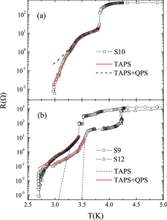
The results of the theoretical interpretation according to Eq. 3 for samples S9 and S12 are reported in Fig. 2(b) by thick red
lines. As far as the sample S12 is concerned, the best fit to the curve obtained with Eq. 3 nicely follows the data, which, on
the other hand strongly deviate from the solely TAPS dependence obtained from the same equation disregarding the QPS term (dashed black line).
These results suggest that the pronounced resistance tail exhibited by sample S12 could indeed originate from QPS processes. On the other hand the
dependence of bridge S9 arising from both TAPS and QPS (Eq. 3) is in agreement with the experimental points only down to K. Below this temperature the curvature of the curve changes again with a slope more consistent with thermal activation.
However, the discrepancy between the TAPS dependence obtained from Eq. 3 considering only the thermal contribution (dashed black line)
and the experimental data is extremely pronounced. It is worth commenting the values of the parameters extracted from the fitting procedure. In
particular the values of the critical temperature, namely K, estimated for samples S9, S10, and S12, respectively, are
close to the measured ones (see Table 2). The best fitting procedures performed with the full Eq. 3 was obtained using , in agreement with the values reported in the literature Bae , but at the price of considering quite high values of . This discrepancy can be possibly attributed to the exponential approximation assumed in treating the QPS contribution. Finally for
sample S10 a value of meV was extracted Kwok . From the relation valid for a single
nanowire in the framework of the approximate phenomenological formula of Arrhenius-Little Bae , following Ref. Kwok , it is possible
to estimate nm.
This analysis reveals that, despite the models were derived for an individual wire, they can reproduce
the transition of networks with not well defined length and, moreover, with finite widths and activation energies distribution. Clearly these
spreads are not taken into account in these models, as well as the distribution of the strengths of the contacts between the nanowires in the
network. Indeed poor contacts, which may be present in these systems for instance at grain boundaries, can behave such weak links, the presence of
which increases the probability of TAPS and QPS Bae . These parameters fluctuations, which are due to the peculiar growth technique of the
network, are expected to affect more the samples with lower values of . In this sense the behavior of sample S12, which is
expected to be more homogeneous compared to sample S9, is better reproduced by Eq. 3. In this respect, however, it is worth commenting
that, since in arrays of small Josephson contacts the thermal activation of the Josephson weak links may also affect the shape of the
curves, the experimental data were also analyzed in the framework of the theory of Ambegaokar and Halperin AmbHal within the formulation
given in Ref. BezrPRB . The procedure revealed an extremely poor agreement between the dependencies and the model for any reasonable
physical value of the fitting parameters, confirming that weak links do not dominate the transport in these systems. Finally, to shed a light on
the physics revealed by these systems two complementary experiments could be performed. On one hand electron beam lithography could be used to
fabricate much narrower bridges, obtaining better controlled arrays with a drastically reduced number of interconnected wires and, consequently, a
narrower distribution of widths and contact strength. Moreover the analysis of the microwave response of the arrays could help to determine the
dominant dissipation process, namely TAPS or QPS Bae .
In summary, both thermal and quantum fluctuations were revealed from measurements in superconducting Nb nanowire networks patterned on PS
substrates. The innovation of the analyzed systems lies both in the widely accessible fabrication technique, which rely on rigid templates, and,
most importantly, in the multiple-connectivity of the wires.
The research leading to these results has received funding from the
European Union Seventh Framework Programme (FP7/2007- 2013) under grant agreement N. 264098 MAMA. The authors wish to thank Prof. A. D. Zaikin
for useful suggestions.
References
- (1) K.Y. Arutyunov, D.S. Golubev, and A.D. Zaikin, Physics Reports 464, 1 (2008).
- (2) A. Bezryadin, J. Phys.: Condens. Matt. 20, 043202 (2008).
- (3) A. Johansson, G. Sambandamurthy, D. Shahar, N. Jacobson, and R. Tenne, Phys. Rev. Lett. 95, 116805 (2005).
- (4) C.N. Lau, N. Markovic, M. Bockrath, A. Bezryadin, and M. Tinkham, Phys. Rev. Lett. 87, 217003 (2001).
- (5) O.V. Astafiev, L.B. Ioffe, S. Kafanov, Yu.A. Pashkin, K.Yu. Arutyunov, D. Shahar, O. Cohen, and J.S. Tsai, Nature 484, 355 (2012).
- (6) J. Ku, V. Manucharyan, and A. Bezryadin, Phys. Rev. B 82, 134518 (2010).
- (7) J.E. Mooij and Yu.V. Nazarov, Nat. Phys. 2, 169 (2006).
- (8) D. Pekker, A. Bezryadin, D.S. Hopkins, and P.M. Goldbert, Phys. Rev. B 308, 1762 (2005).
- (9) A. Bezryadin, Nature 484, 324 (2012).
- (10) N. Giordano, Phys. Rev. B 41, 6350 (1990).
- (11) A.T. Bollinger, A. Rogachev, M. Remeika, and A. Bezryadin, Phys. Rev. B 69, 180503(R) (2004).
- (12) M. Zgirsti and K.Yu. Arutyunov, Phys. Rev. B 75, 172509 (2007).
- (13) U. Patel, Z. L. Xiao, A. Gurevich, S. Avci, J. Hua, R. Divan, U. Welp, and W. K. Kwok, Phys. Rev. B 80, 012504 (2009).
- (14) R.S. Newbower, M.R. Beasley, and M. Tinkham, Phys. Rev. B 5, 864 (1972).
- (15) J. Wang, X.-C. Ma, L. Lu, A.-Z. Jin, C.-Z. Gu, X.C. Xie, J.-F. Jia, X. Chen, and Q.-K. Xue, Appl. Phys. Lett. 92, 233119 (2008).
- (16) A. Bezryadin, C.N. Lau, and M. Tinkham, Nature 404, 971 (2000).
- (17) D.S. Hopkins, D. Pekker, P.M. Goldbert, and A. Bezryadin, Science 308, 1762 (2005).
- (18) A. Bezryadin and P.M. Goldbart, Adv. Mater. 22, 1111 (2010).
- (19) G. Yi and W. Schwarzacher, Appl. Phys. Lett. 74, 1746 (1999).
- (20) S. Michotte, L. Piraux, S. Dubois, F. Pailloux, G. Stenuit, and J. Govaerts, Physica C 377, 267 (2002).
- (21) M. Tian, J. Wang, J.S. Kurtz, Y. Liu, M.H.W. Chan, T.S. Mayer, and T.E. Mallouk, Phys. Rev. B 71, 104521 (2005).
- (22) Q. Luo, X.Q. Zeng, M.E. Miszczak, Z.L. Xiao, J. Pearson, T. Xu, and W.K. Kwok, Phys. Rev. B 85, 174513 (2012).
- (23) A.D. Zaikin, D.S. Golubev, A. van Otterlo, and G.T. Zimnyi, Phys. Rev. Lett. 78, 1552 (1997); D.S. Golubev and A.D. Zaikin, Phys. Rev. B 64, 014504 (2001).
- (24) D.S. Golubev and A.D. Zaikin, Phys. Rev. B. 78, 144502 (2008).
- (25) M.-H. Bae, R.C. Dinsmore III, T. Aref, M. Brenner, and A. Bezryadin, Nano Lett. 9, 1889 (2009).
- (26) M. Trezza, S.L. Prischepa, C. Cirillo, R. Fittipaldi, M. Sarno, D. Sannino, P. Ciambelli, M.B.S. Hesselberth, S.K. Lazarouk, A.V. Dolbik, V.E. Borisenko, and C. Attanasio, J. Appl. Phys. 104, 083917 (2008).
- (27) M. Trezza, C. Cirillo, S.L. Prischepa, and C. Attanasio, Europhys. Lett. 88, 57006 (2009).
- (28) G. Ausanio, V. Iannotti, S. Amoruso, X. Wang, C. Aruta, M. Arzeo, R. Fittipaldi, A. Vecchione, R. Bruzzese, and L. Lanotte, Appl. Surf. Sci. 258, 9337 (2012).
- (29) J.S. Lehtinen, T. Sajavaara, K.Yu. Arutyunov, M.Yu. Presnjakov, and A.L. Vasiliev, Phys. Rev. B. 85, 094508 (2012).
- (30) C. Cirillo and C. Attanasio, (private communication).
- (31) M.S.M. Minhaj, S. Meepagala, J.T. Chen, and L.E. Wenger, Phys. Rev. B 49, 15235 (1994).
- (32) A. Rogachev and A. Bezryadin, Appl. Phys. Lett. 83, 512 (2003).
- (33) P. Sabatino, C. Cirillo, G. Carapella, M. Trezza, and C. Attanasio, J. Appl. Phys. 108, 053906 (2010).
- (34) H.S.J. van der Zant, M.N. Webster, J. Romijn, and J.E. Mooij, Phys. Rev. B. 50, 340 (1994).
- (35) M.Y. Kupriyanov and V.F. Lukichev, Fiz. Nizk. Temp. 6, 445 (1980) [Sov. J. Low Temp. Phys. 6, 210 (1980)].
- (36) V. Ambegaokar and B.I. Halperin, Phys. Rev. Lett. 22, 1364 (1969).