Electronic, Magnetic and Transport Properties of Graphene Ribbons Terminated by Nanotubes
Abstract
We study by density functional and large scale tight-binding transport calculations the electronic structure, magnetism and transport properties of the recently proposed graphene ribbons with edges rolled to form nanotubes. Edges with armchair nanotubes present magnetic moments localized either in the tube or the ribbon and metallic or half-metallic character, depending on the symmetry of the junction. These properties have potential for spin valve and spin filter devices with advantages over other proposed systems. Edges with zigzag nanotubes are either metallic or semiconducting without affecting the intrinsic mobility of the ribbon. By varying the type and size of the nanotubes and ribbons offers the possibility to tailor the magnetic and transport properties, making these systems very promising for applications.
The atomic structure of graphene edges is important for the determination of the electronic and magnetic properties of graphene, especially for narrow graphene nanoribbons[1, 2, 3, 4, 5, 6, 7, 8, 9, 10, 11, 12]. Recent theoretical work[13] on the stability of different graphene edges structures has shown that graphene edges can fold back on themselves and reconstruct as nanotubes, with low formation energy (see atomic structures in figure 1). In this article, we show that, beside protecting the edges from contamination and reconstructions, nanotubes at the edges may lead to magnetism and are not detrimental for the electronic mobility despite the row of hybridized atoms at the ribbon-tube junction. We study the electronic and magnetic properties of these systems by a combination of density functional theory (DFT) and large scale tight binding (TB) simulations of transport properties. Our calculations suggest that these systems could be used for a variety of applications that we sketch in figure 2.
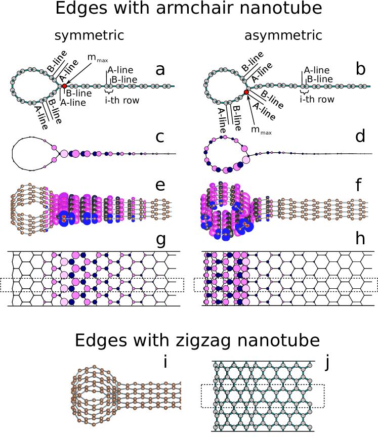
We consider systems formed by a nanoribbon terminated on both sides by the same armchair (AC) or zigzag (ZZ) nanotube. We notice that a ribbon with AC edges is terminated by ZZ nanotubes and a ribbon with ZZ edges is terminated by AC nanotubes. Nanoribbons terminated by AC nanotubes present interesting magnetic properties. By rolling the ZZ edges of a nanoribbon, two types of AC nanotubes can be formed, as shown in figure 1. If the atoms at the nanoribbon ZZ edge scroll and bind to the same sublattice sites within the nanoribbon, the formed AC nanotube has mirror symmetry with respect to the nanoribbon plane; if the bonding sites belong to opposite sublattice, there is no such kind of symmetry (compare figure 1b to figure 1a). We call these two cases symmetric and asymmetric which corresponds to armchair and armchair-like in Ref. [13], respectively. The common point of these two cases is that the sublattice symmetry is broken, because all the hybridized carbon atoms at the junction belong to one sublattice. Due to Lieb theorem [8, 12], this gives the possibility of spin polarization around the junctions. Since the theorem applies to the Hubbard model, accurate calculations for the real system are necessary to investigate this possibility.
| N | P | S (symmetric) | S (asymmetric) |
|---|---|---|---|
| 9 | 4 | 0.000 | 1.499 |
| 8 | 8 | 0.995 | 1.499 |
| 7 | 12 | 1.371 | 1.499 |
| 6 | 16 | 1.481 | 1.499 |
| 5 | 20 | 1.500 | 1.500 |
| 4 | 24 | 1.500 | 1.500 |
| 3 | 28 | 1.494 | 1.500 |
In order to study the magnetic properties, we performed spin polarized DFT calculations by SIESTA[14, 15, 16]. We used generalized gradient approximation with Perdew-Burke-Ernzerhof parametrization (GGA-PBE) [17] and a standard built-in double- polarized (DZP) [18] basis set to perform geometry relaxation. We found that, in both symmetric and asymmetric cases, there is spin polarization near the ribbon-tube junction, i.e., near the hybridized carbon atoms. Note that the bond distance of these four-fold coordinated atoms is Å like in diamond. The spin polarization is mainly located in the nanoribbon for the symmetric case and within the tube for the asymmetric case (see the isosurface plot of the spin density together with its symbolic representation in figure 1c-h). The up/down spins are distributed over the A/B sublattices respectively. The label indicates the atom with the highest magnetic moment.
For the symmetric case, the value of the spin polarization increases with increasing nanoribbon width, and saturates at 1.50 per unit cell, when the nanoribbon width is wider than 16 ZZ rows; For the asymmetric case, the spin polarization is always 1.50 per unit cell, irrespective of the nanoribbon width and nanotube radius (see Table 1).
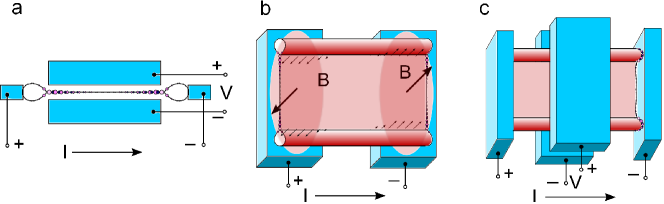
For the asymmetric case the spins are located inside the two nanotubes and therefore the exchange interaction between opposite edges is negligible. For the symmetric case, the spins on the two edges are coupled antiferromagnetically, similarly to hydrogen terminated graphene edges[20, 21]: for the structure shown in figure 1a, the energy of antiparallel spin configurations is meV per unit cell (see figure 1g) lower than for parallel configurations. This sizeable coupling across the ribbon makes the symmetric systems promising as spin valve devices[22]. In figure 2a we show a configuration similar to that proposed for dumbbell graphene structures on the basis of the Hubbard Hamiltonian in the mean field approximation[23]. A gate could be used to bring the system from the antiferromagnetically coupled state to the ferromagnetically coupled excited state, favouring spin transport from one nanotube to the other across the ribbon. Moreover, both for the symmetric and asymmetric case, the magnetic moments along the ribbon-tube junction are qualitatively similar to the case of ZZ edges of nanoribbons. Therefore, high magnetoresistance could be expected, as proposed in [19] for nanoribbons with ZZ edges, by applying magnetic fields of different sign at the ends of the nanoribbon. A sketch of this device for our systems is shown in figure 2b.
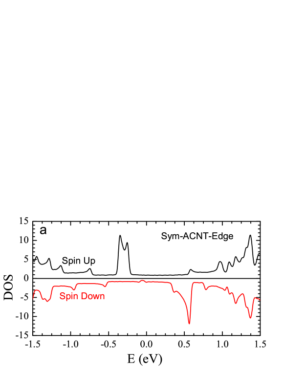
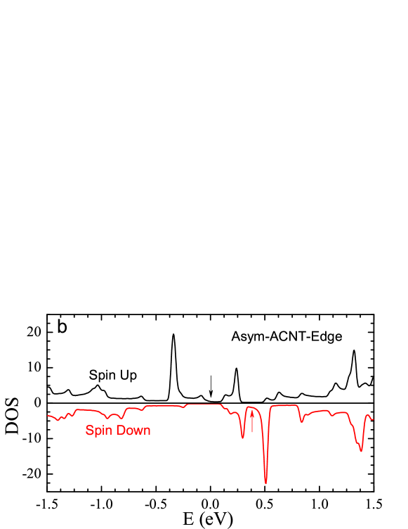
The spin polarized density of states (DOS) reveals other features of interest for spintronics related to half-metallic character. In figure 3a and 3b we show the spin polarized DOS for the symmetric and asymmetric case respectively. We see that the symmetric case is metallic for both spins in the whole range of energy. The asymmetric case, instead, is a half-metal near the Fermi energy , namely it is metallic for spin up and insulating for spin down. The half-metallic character of our systems provides opportunities as spin filters without the need of external electric fields[24], magnetic fields[25], ferromagnetic strips[26], impurities[27, 28, 29] or defects[30, 31]. Furthermore, there is the opposite half-metallic character at higher energies. Around 0.4 eV, there is insulating character for spin up and metallic character for spin down. As sketched in figure 2c, a gate along the ribbon could be used to switch between these two half-metallic energy regions and affect selectively the spin transport.
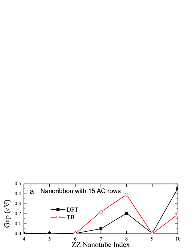
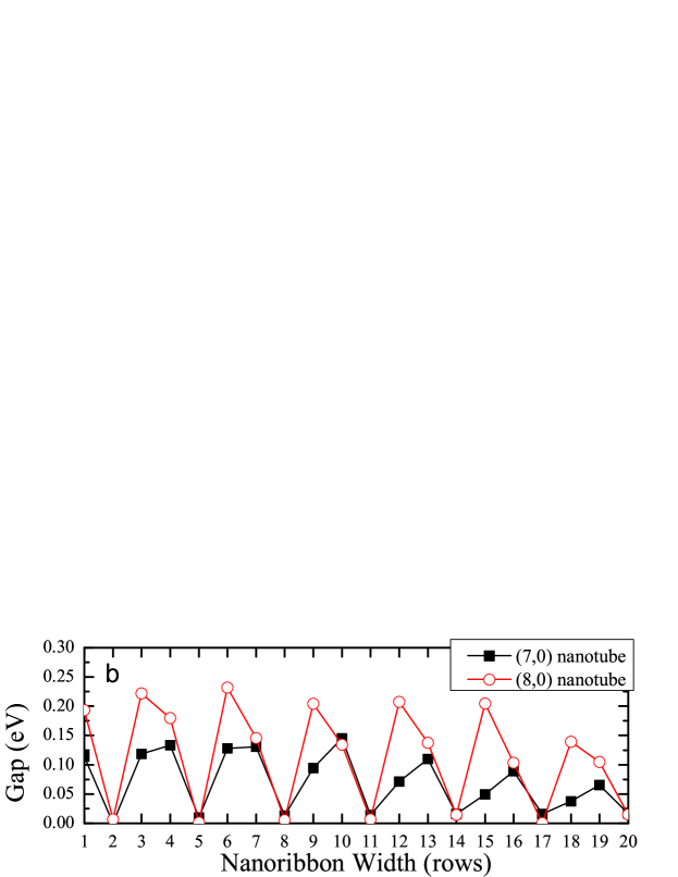
We come now to the case with ZZ nanotubes shown in figure 1i-j. For this case, there is only one type of ribbon-tube junction that preserves sublattice symmetry implying that there is no magnetization nor midgap states[8, 12]. The electronic structure and transport properties, however, strongly depend on the AC ribbon width and on the ZZ tube radius. In TB models, a AC nanoribbon is metallic if the number of AC rows is equal to , where is a positive integer, and semiconducting otherwise[1, 32]. Furthermore, ZZ nanotubes are metallic for index equal to [33]. In more general models, the properties of AC nanoribbons and ZZ nanotubes may differ from the ones predicted by TB, due to possible self passivation of the edges for nanoribbons and for the band mixing for small nanotubes[33]. By using DFT calculations, we found that our joined system becomes a semiconductor with a gap of the order of few hundreds meV if both nanoribbon and nanotube are semiconducting. The energy gap as a function of geometry is shown in figure 4. The size of the nanotube has to be large enough for the opening of a band gap (figure 4a). For the joined system with semiconducting ZZ nanotubes, there is a clear periodicity (3 ZZ rows) in the dependence of the energy gap on the nanoribbon width (figure 4b). For the studied cases, the value of the gap varies between 30 and 600 meV.
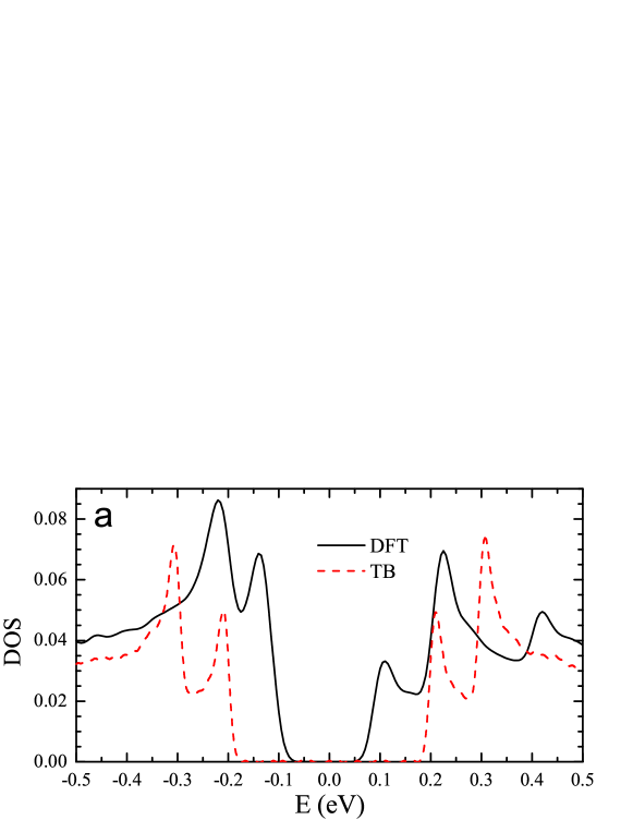
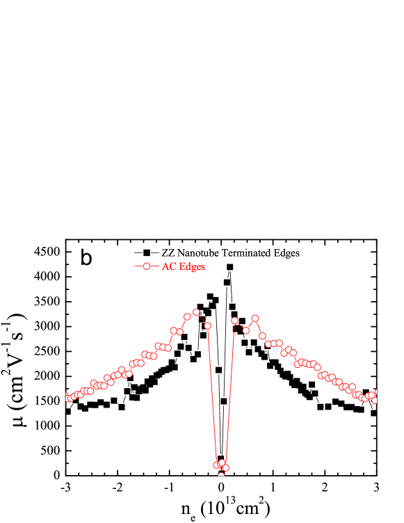
Since we want to calculate the transport properties by means of a simpler model, suitable for large samples, we have also calculated the energy structure of our system by -band TB calculations where we consider only the nearest-neighbor hopping eV between the carbon atoms[34, 35] for all bonds. The comparison between the gaps calculated by TB and DFT shown in figure 4a gives the same periodicity and a qualitative agreement. For the case of a AC nanoribbon with 15 rows terminated by (8,0) ZZ nanotubes we compare in figure 5a the TB and DFT DOS, which again are in qualitative agreement as to support the validity of the transport calculations we show next. The electronic transport properties of a semiconducting nanoribbon with or without nanotube terminated edges are obtained by using large scale TB simulations with about thirty million carbon atoms[34, 35]. In figure 5b we show that the electronic mobility parallel to the edges as a function of charge density are quite similar in these two cases. The mobility of the joined system is about at charge density , which is only slightly smaller than the one of the AC nanoribbon at the same charge concentration.
In summary, we have studied the electronic and magnetic properties of graphene nanoribbons with three types of nanotube terminated edges. The spin magnetization is found to be 1.5 per unit cell in the ground state of both symmetric and asymmetric AC nanotube terminated edges. For symmetric AC nanotube terminated edges, the spin density is located in the ribbon whereas, for the asymmetric case, it is located within the tube. In the ZZ nanotube terminated edges, there is a band gap opening of the order of few hundreds meV, if the constituent tube and nanoribbon are both semiconducting. The conductivity and mobility in the presence of ZZ nanotube terminated edges is comparable to the one of the AC nanoribbon itself.
Our calculations suggest that these systems are not only advantageous because the edges are protected against any kind of chemically induced disorder but also because, by tailoring the ribbon/tube structure, they offer a wealth of possible applications for transport and spintronics.
Acknowledgments
The support by the Stichting Fundamenteel Onderzoek der Materie (FOM) and the Netherlands National Computing Facilities foundation (NCF) are acknowledged. We thank the EU-India FP-7 collaboration under MONAMI and the grant CONSOLIDER CSD2007-00010.
References
References
- [1] Son Y W, Cohen M L and Louie S G 2006 Phys. Rev. Lett. 97(21) 216803
- [2] Han M Y, Özyilmaz B, Zhang Y and Kim P 2007 Phys. Rev. Lett. 98(20) 206805
- [3] Koskinen P, Malola S and Häkkinen H 2008 Phys. Rev. Lett. 101(11) 115502
- [4] Wassmann T, Seitsonen A P, Saitta A M, Lazzeri M and Mauri F 2008 Phys. Rev. Lett. 101(9) 096402
- [5] Girit C O, Meyer J C, Erni R, Rossell M D, Kisielowski C, Yang L, Park C H, Crommie M F, Cohen M L, Louie S G and Zettl A 2009 323 1705–1708
- [6] Liu Z, Suenaga K, Harris P J F and Iijima S 2009 Phys. Rev. Lett. 102(1) 015501
- [7] Wimmer M, Akhmerov A R and Guinea F 2010 Phys. Rev. B 82(4) 045409
- [8] Yazyev O V Reports on Progress in Physics 73 056501
- [9] van Ostaay J A M, Akhmerov A R, Beenakker C W J and Wimmer M 2011 Phys. Rev. B 84(19) 195434
- [10] Jia X, Campos-Delgado J, Terrones M, Meunier V and Dresselhaus M S 2011 Nanoscale 3(1) 86–95
- [11] Kunstmann J, Özdoğan C, Quandt A and Fehske H 2011 Phys. Rev. B 83(4) 045414
- [12] Katsnelson M I 2012 Graphene: Carbon in Two Dimensions (Cambridge University Press)
- [13] Ivanovskaya V V, Zobelli A, Wagner P, Heggie M I, Briddon P R, Rayson M J and Ewels C P 2011 Phys. Rev. Lett. 107(6) 065502
- [14] Soler J M, Artacho E, Gale J D, Garcia A, Junquera J, Ordejon P and Sanchez-Portal D 2002 J. Phys.: Condens. Matter 14 2745–2779
- [15] Sanchez-Portal D, Ordejon P and Canadell E 2004 Principles and Applications of Density functional Theory in Inorganic Chemistry II 113 (Berlin: Springer)
- [16] Artacho E, Anglada E, Dieguez O, Gale J D, Garcia A, Junquera J, Martin R M, Ordejon P, Pruneda J M, Sanchez-Portal D and Soler J M 2008 J. Phys.: Condens. Matter 20 064208
- [17] Perdew J P, Burke K and Ernzerhof M 1996 Phys. Rev. Lett. 77
- [18] Junquera J, Paz O, Sánchez-Portal D and Artacho E 2001 Phys. Rev. B 64
- [19] Kim W Y and Kim K S 2008 Nature Nanotech. 3 408–412 ISSN 1748-3387
- [20] Yazyev O V and Katsnelson M I 2008 Phys. Rev. Lett. 100
- [21] Bhandary S, Eriksson O, Sanyal B and Katsnelson M I 2010 Phys. Rev. B 82
- [22] Hill E W, Geim A K, Novoselov K, Schedin F and Blake P 2006 IEEE Trans. Magn. 42 2694–2696 ISSN 0018-9464 41st IEEE International Magnetics Conference (Intermag 2006), San Diego, CA, MAY 08-12, 2006
- [23] Ma Z and Sheng W 2011 Appl. Phys. Lett. 99(8) 083101
- [24] Son Y W, Cohen M L and Louie S G 2006 Nature 444 347–349
- [25] Abanin D A, Lee P A and Levitov L S 2006 Phys. Rev. Lett. 96(17) 176803
- [26] Zhang Y T, Jiang H, Sun Q f and Xie X C 2010 Phys. Rev. B 81(16) 165404
- [27] Hod O, Barone V, Peralta J E and Scuseria G E 2007 Nano Lett. 7 2295–2299
- [28] Zheng X H, Wang R N, Song L L, Dai Z X, Wang X L and Zeng Z 2009 Appl. Phys. Lett. 95
- [29] Soriano D, Muñoz Rojas F, Fernández-Rossier J and Palacios J J 2010 Phys. Rev. B 81(16) 165409
- [30] Martins T B, da Silva A J R, Miwa R H and Fazzio A 2008 Nano Lett. 8 2293–2298
- [31] Lisenkov S, Andriotis A N and Menon M 2012 Phys. Rev. Lett. 108(18) 187208
- [32] Ezawa M 2006 Phys. Rev. B 73(4) 045432
- [33] Dubois S M M, Zanolli Z, Declerck X and Charlier J C 2009 Eur. Phys. J. B 72
- [34] Wehling T O, Yuan S, Lichtenstein A I, Geim A K and Katsnelson M I 2010 Phys. Rev. Lett. 105 056802
- [35] Yuan S, De Raedt H and Katsnelson M I 2010 Phys. Rev. B 82 115448