Prediction of semi-metallic tetragonal and from first-principles
Abstract
A tetragonal phase is predicted for and using density functional theory. Starting from atomic and unit cell relaxations of substoichiometric monoclinic and , such tetragonal structures are only reached at zero temperature by introducing the oxygen vacancy pair with the lowest formation energy. The tetragonal and structures belong to space group and are more stable than their corundum structure counterparts. These phases are semi-metallic, as confirmed through further calculations. The carrier concentrations are estimated to be for both electrons and holes in tetragonal , and for both electrons and holes in tetragonal . The tetragonal phase is probably related to the low resistivity state of hafnia-based resistive random access memory (RRAM).
Hafnia () and zirconia () are found in a number of important technological applications.Lange, ; Kilner, In particular, hafnia has become a key component in sub-micrometer silicon MOS technology as the current choice of high permittivity dielectric layer.Robertson2006, In addition, it is also a promising candidate material for resistive random access memory (RRAM), which is one of the leading technologies for the next-generation non-volatile memory.Asamitsu, ; Ignatiev, ; Waser2007, ; Kope, The core element of RRAM is a metal/insulator/metal capacitor which is subject to an electroforming process, where a high electric field (some MV/cm) is applied across the capacitor to create conduction paths in the insulating thin film, here named filaments. These filaments are of unknown composition or shape, and can be easily disturbed under electrical stress, leading to a memory effect. Knowing the composition of the filaments is crucial to the understanding of RRAM’s physics. Previous work on RRAM reveals that the conductive filament is possibly due to Magnéli phases, where the value of is mostly 4 or 5.Ti4O7, For hafnia RRAM, the structure of the conductive filaments has not been reported, though it is widely accepted that the filaments are associated to an oxygen-deficient phase.Lin2011, ; Kamiya, Since the impact of electroforming is expected to occur in small and random patches of the capacitor, experimental investigation of the filaments suffers from great difficulty.
In the present paper we employ first-principles density functional theoryDFT, (DFT) calculations to identify O-poor stable compositions of hafnium and zirconium oxides which may be reachable from the room temperature normal pressure monoclinic [-] with the assistance of an external source of energy, possibly an applied electric field. The processing and operation of oxide-based RRAM (OXRRAM) stimulated our search of a conductive phase in these materials. However, our predictions are quite general and may have broader implications.
For DFT calculations, plane-wave based Vienna Ab initio Simulation Package (VASP) programVASP, was implemented, using projector-augmented-wave (PAW) pseudopotentialsPAW, with Hf , and (Zr , , and ) electrons and O and electrons in the valence. Generalized gradient approximation (GGA) was used for the exchange-correlation energy, within the Perdew-Burke-Ernzerhof (PBE) functional.PBE, The plane wave energy cutoff is chosen as 500 eV which converges for all the involved compounds, and sufficiently dense Monkhorst-PackMonkhorst, or -centered -mesh was utilized for sampling the Brillouin zone.
Because DFT/GGA usually underestimates band gaps, and may even deem a material metallic rather than semiconductor as the case of bulk germanium,Germanium, for the metallic or semi-metallic candidates we calculated the first order energy shifts with approximationGW, () using the ABINITAbinit, ; VASP-Abinit, program. Hf (Zr) semi-core electrons were explicitly included through the () configuration while core electrons were replaced by Troullier-Martins pseudopotentials.TMPP, Convergence was achieved with 360 bands and a 15 Ha cutoff for the wave functions employed in the evaluation of the dielectric function and the function. A plasmon-pole approximationPlasmon, was used.
The - unit cells were fully relaxed until all Hellmann-Feynman forces were less than 0.01 eV/Å and all stresses were less than 400 MPa. The relaxed - unit cell parameters are a=5.146 (5.219) Å, b/a=1.010 (1.012), c/a=1.036 (1.036) and (), close to experimental values:Exp-Lattice, a=5.117 (5.151) Å, b/a=1.011 (1.010), c/a=1.034 (1.032) and (). The formation enthalpy of - calculated with respect to Hf (Zr) and an isolated molecule is -1166 (-1106) kJ/mol, after adopting the 1.36 eV energy correction for the molecule provided by Wang et al.Ceder2006, These results are in accord with the experimental values, which are -1145 kJ/mol for hafnia and -1101 kJ/mol for zirconia.Speight,
For reference we first calculated the formation energies of single and double oxygen vacancies in a 96-atom - supercell (). Aiming at energetically favorable metallic phases, only the neutral oxygen vacancy was considered. There are two inequivalent O sites regarding O coordination, namely the 3- and 4-coordinated O(A) and O(B) sites, respectively. The formation energy of a neutral oxygen vacancy is defined as
| (1) |
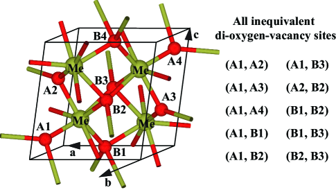
where is the energy of the defective supercell, is the energy of the defect-free supercell and is the chemical potential of oxygen. Under oxygen-rich condition is usually set as one half of that of an molecule. In this case the calculated for a neutral O(A) vacancy in - is 7.13 (6.62) eV, while for a neutral O(B) vacancy it is 7.00 (6.53) eV. The difference between the two formation energies, 0.13 (0.09) eV, is similar to Zheng et al.,Ceder2007, but larger than Foster et al. who reported a 0.02 eV difference in both cases.Foster2001, ; Foster2002, Next we calculated the formation energies of di-oxygen-vacancy pairs in -. To this end, the 8 oxygen sites in a unit cell were named A1–A4 and B1–B4, as shown in Fig. 1. The distance between two di-oxygen-vacancy pairs is around 10 Å, casting them as isolated pairs. Since - possesses the baddeleyite structure with space group , there are 10 inequivalent di-oxygen-vacancy pairs. The most energetically favorable pair is the (B1, B2) pair, whose formation energy per vacancy is the same as of a single O(B) vacancy.
Under usual experimental conditions the dielectric is placed between two metal electrodes where oxygen can migrate as an interstitial. We thus calculated the incorporation energies of oxygen, starting from its molecular form, into bulk Ti and Pt, two commonly used electrodes. The results are -6.24 eV and 0.91 eV, respectively. The formation energies of single and double oxygen vacancy in all three environments are thus compared in Tab. \@slowromancapi@. Notice that the formation energy of a neutral O(B) vacancy in - plus an oxygen interstitial in Ti is merely 0.76 (0.29) eV, which is attributed to the strong Ti–O bonding.
| Chemical | Vacancy | Supercell | Formation energy (eV/vacancy) | ||
| formula | site(s) | units | with oxygen going to | ||
| Ti | Pt | ||||
| Single oxygen vacancy | |||||
| O(A) | 222 | 7.13(6.62) | 0.89(0.38) | 8.04(7.53) | |
| O(B) | 222 | 7.00(6.53) | 0.76(0.29) | 7.91(7.44) | |
| Closest di-oxygen-vacancy | |||||
| (B1, B2) | 222 | 7.01(6.52) | 0.77(0.28) | 7.92(7.43) | |
| (B2, B3) | 222 | 7.02(6.60) | 0.78(0.36) | 7.93(7.51) | |
| (A1, B1) | 222 | 7.03(6.53) | 0.79(0.29) | 7.94(7.44) | |
| O(A) | 111 | 7.16(6.66) | 0.92(0.42) | 8.07(7.57) | |
| O(B) | 111 | 7.03(6.57) | 0.79(0.33) | 7.94(7.48) | |
| (B1, B2) | 111 | 6.55(5.66) | 0.31(-0.58) | 7.46(6.57) | |
| (A1, B1) | 111 | 6.92(6.40) | 0.68(0.16) | 7.83(7.31) | |
| (B2, B3) | 111 | 6.95(6.33) | 0.71(0.09) | 7.86(7.24) | |
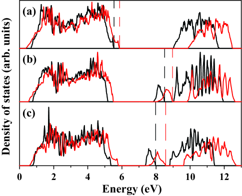
The search for metallic states began with the models generated by introducing one oxygen vacancy per 12-atom - for two inequivalent cases, i.e., O(A) and O(B). The defective unit cells were fully relaxed until all Hellmann-Feynman forces were less than 0.01 eV/Å. Atomic coordinates, cell dimensions and shape were subject to relaxation. The formation energies per vacancy of the two phases are almost the same as in the single oxygen vacancy cases. The resulting DOS are shown in Figs. 2(b) and 2(c). In either case, a fully occupied defect-induced band emerges in the band gap, indicating a semiconductor. While the DOS of this band is broad and high, it cannot account for the measured metallic state in hafnia-based RRAM, because in that state the resistance is on the order of hundreds of Ohms for 10 nm thin films.Leti2011, However, the trend does hint that stronger off-stoichiometric hafnia or zirconia might undergo a phase transition from dielectric to metal.
| Bulk modulus | |||||
|---|---|---|---|---|---|
| 3.135 Å | 5.646 Å | 0.2553 | 0.1351 | 246 GPa | |
| 3.174 Å | 5.763 Å | 0.2525 | 0.1367 | 228 GPa |
Hence, several models were set up with two oxygen vacancies per 12-atom - unit cell. For all inequivalent cases (Fig. 1) the cells remain monoclinic during relaxation of the unit cell vectors, except for the (B1, B2) case which suffers from a monoclinic-to-tetragonal transition. The tetragonal [-] phase (Fig. 3; structural parameters in Tab. \@slowromancapii@) is the ground state of all ten candidates. It belongs to the point group and (No. 115) space groupAroyo, . The Hf(Zr) coordination number is 7 as in -, while 2/3 of the oxygen sites have coordination number 5 [named O(A)] and 1/3 have coordination number 4 [named O(B)]. Symmetry analysis indicates that Hf(Zr) and O(A) are at the position while O(B) is at the positionBilbao, . The average Hf(Zr)–O(A) and Hf(Zr)–O(B) bond lengths are 2.295 (2.322) Å and 2.089 (2.134) Å, respectively, compared with 2.084 (2.117) Å and 2.209 (2.240) Å in -. Bader analysis reveals that the Hf (Zr) charge changes from 2.73e (2.57e) in - to 2.10e (2.02e) in -; the O(A) charge changes from -1.34e (-1.25e) to -1.39e (-1.34e); and the O(B) charge changes from -1.39e (-1.31e) to -1.41e (-1.37e).
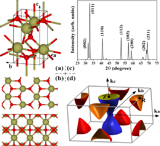
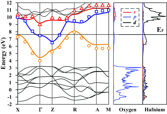
Figure 4 shows the band diagram and orbital-projected DOS of -. Results for - (not shown) are similar. The high symmetry points in the Brillouin zone are named according to the Bilbao crystallographic server.Aroyo, A semi-metallic behavior is revealed in the overlap of the partially occupied valence band top and conduction band bottom located at different high symmetry points, R and Z. Both band edges are mostly derived from Hf states. The semi-metallic character of the two compounds was confirmed by calculations of the many-body correction to the DFT/GGA energy levels. Figure 4 implies that the energy shifts are of the order of a few tenths of eV, retaining the semi-metallic nature of -. The energy shifts obtained for (not shown) are similar. From the calculated band structures the densities of conduction electrons and holes can be obtained by integrating the electron occupation of the blue and orange bands in Fig. 4, respectively. The electron and hole densities are both for -, and both for -, typical of semi-metals.
To evaluate the relative stability of this structure, we calculated the molar formation enthalpy of various , and models with respect to their corresponding metals and . Still, the 1.36 eV energy correction to was applied to all cases. The formation enthalpy of - is -1700 (-1666) kJ/mol, more favorable than fully relaxed corundum , -1586 (-1580) kJ/mol. Nevertheless, a fully relaxed arranged in the tetragonal structure, possesses a formation enthalpy of -1576 kJ/mol, less favorable than corundum whose formation enthalpy is -1598 kJ/mol. These data confirm that for the tetragonal structure is preferred, while for the corundum structure is preferred.
To our best knowledge, the proposed - and - structures have not been reported before, though some published data may suggest their existance. Hildebrandt et al.Frankfurt, performed high-resolution transmission electron microscopy of a conducting thin film where the enlarged inverse Fourier-transformed images show a similar structure as in Fig. 3(b). Manory et al.Osaka, discovered two unidentified X-ray diffraction (XRD) peaks at and in hafnia films grown by ion beam assisted deposition at a transport ratio of 5 and an ion energy of 20 keV. They attributed these peaks to a new tetragonal structure and suggested the stoichiometry. However, they simulated their data with a phase with lattice parameters a=5.055 Å and c=5.111 Å, resulting in two small peaks around . We calculated powder XRD patternsXRD, for - [Fig. 3(d)] using Cu radiation ( Å), and found a (110) peak at and a (112) peak at , similar to data. Similar calculation for - yielded a (110) peak at and a (112) peak at .
In conclusion, we have predicted tetragonal semi-metallic and structures as the ground state highly oxygen deficient hafnia and zirconia which undergo a monoclinic-to-tetragonal phase transition. Their semi-metallic properties are characterized by an overlap of the valence band maximum and conduction band minimum at different points of the Brillouin zone, and by the low density of conduction electrons and holes. Also, - may be the physical origin of the conductive state in hafnium-based RRAM.
This work is financially supported by the Nanosciences Foundation of Grenoble (France) in the frame of the Chairs of Excellence awarded to L.R.C. Fonseca in 2008 and to Y. Nishi in 2010. LRCF also acknowledges CNPq for financial support. The calculations were performed on the Stanford NNIN (National Nanotechnology Infrastructure Network) Computing Facility funded by the National Science Foundation of USA. We specially thank Dr. Blanka Magyari-Köpe from Stanford University for pointing out the experimental results in Ref. Osaka, .
References
- (1) S. Lange, V. Kiisk, V. Reedo, M. Kirm, J. Aarik, and I. Sildos, Opt. Mater. 28, 1238 (2006).
- (2) J. A. Kilner, Nat. Mater. 7, 838 (2008).
- (3) J. Robertson, Rep. Prog. Phys. 69, 327 (2006).
- (4) A. Asamitsu, Y. Tomioka, H. Kuwahara, and Y. Tokura, Nature 388, 50 (1997).
- (5) S. Q. Liu, N. J. Wu, and A. Ignatiev, Appl. Phys. Lett. 76, 2749 (2000).
- (6) R. Waser and M. Aono, Nat. Mater. 6, 833 (2007).
- (7) B. Magyari-Köpe, M. Tendulkar, S.-G. Park, H. D. Lee, and Y. Nishi, Nanotechnology 22, 254029 (2011).
- (8) D.-H. Kwon, K. M. Kim, J. H. Jang, J. M. Jeon, M. H. Lee, G. H. Kim, X.-S. Li, G.-S. Park, B. Lee, S. Han, M. Kim, and C. S. Hwang, Nat. Nanotechnol. 5, 1748 (2010).
- (9) K.-L. Lin, T.-H. Hou, J. Shieh, J.-H. Lin, C.-T. Chou, and Y.-J. Lee, J. Appl. Phys. 109, 084104 (2011).
- (10) K. Kamiya, M. Y. Yang, S.-G. Park, B. Magyari-Kope, Y. Nishi, M. Niwa, and K. Shiraishi, Appl. Phys. Lett. 100, 073502 (2012).
- (11) P. Hohenberg and W. Kohn, Phys. Rev. 136, B864 (1964); W. Kohn and L. J. Sham, Phys. Rev. 140, A1133 (1965).
- (12) G. Kresse and J. Furthmüller, Comput. Mater. Sci. 6, 15 (1996); Phys. Rev. B 54, 11169 (1996).
- (13) P. E. Blöchl, Phys. Rev. B 50, 17953 (1994); G. Kresse and D. Joubert, Phys. Rev. B 59, 1758 (1999).
- (14) J. P. Perdew, K. Burke, and M. Ernzerhof, Phys. Rev. Lett. 77, 3865 (1996).
- (15) P. Broqvist, A. Alkauskas, and A. Pasquarello, Phys. Rev. B 78, 075203 (2008).
- (16) L. Hedin, Phys. Rev. 139, A796 (1965).
- (17) F. Bruneval, N. Vast, and L. Reining, Phys. Rev. B 74, 045102 (2006).
- (18) The DFT/GGA band structures obtained with the VASP and ABINIT codes differ by less than 10 meV, justifying the application of energy shifts obtained with ABINIT to the VASP eigenvalues.
- (19) N. Troullier and J. L. Martins, Phys. Rev. B 43, 1993 (1991).
- (20) R. W. Godby and R. J. Needs, Phys. Rev. Lett. 62, 1169 (1989).
- (21) H. J. Monkhorst and J. D. Pack, Phys. Rev. B 13, 5188 (1976).
- (22) R. E. Hann, P. R. Suitch, and J. L. Pentecost, J. Am. Ceram. Soc. 68, C-285 (1985).
- (23) J. G. Speight, Lange’s Handbook of Chemistry, 16th Ed., McGraw-Hill, New York, USA (2004).
- (24) B. Hammer, L. B. Hansen, and J. K. Nørskov, Phys. Rev. B 59, 7413 (1999).
- (25) L. Wang, T. Maxisch, and G. Ceder, Phys. Rev. B 73, 195107 (2006).
- (26) J. X. Zheng, G. Ceder, T. Maxisch, W. K. Chim, and W. K. Choi, Phys. Rev. B 75, 104112 (2007).
- (27) A. S. Foster, V. B. Sulimov, F. L. Gejo, A. L. Shluger, and R. M. Nieminen, Phys. Rev. B 64, 224108 (2001).
- (28) A. S. Foster, F. L. Gejo, A. L. Shluger, and R. M. Nieminen, Phys. Rev. B 65, 174117 (2002).
- (29) C. Cagli et al., IEEE IEDM Tech. Dig., 658 (2011).
- (30) Structures drawn by VESTA: K. Momma and F. Izumi, J. Appl. Crystallogr. 44, 1272 (2011); Fermi surface drawn by XCrySDen: A. Kokalj, Comp. Mater. Sci. 28, 155 (2003).
- (31) M. I. Aroyo, J. M. Perez-Mato, C. Capillas, E. Kroumova, S. Ivantchev, G. Madariaga, A. Kirov and H. Wondratsechek, Z. Kristallogr. 221, 15 (2006).
- (32) http://www.cryst.ehu.es/cgi-bin/cryst/programs/nph-wp-list?gnum=115.
- (33) E. Hildebrandt, J. Kurian, M. M. Müller, T. Schroeder, H.-J. Kleebe, and L. Alff, Appl. Phys. Lett. 99, 112902 (2011).
- (34) R. R. Manory, T. Mori, I. Shimizu, S. Miyake, and G. Kimmel, J. Vac. Sci. Technol. A 20, 549 (2002).
- (35) J. Rodríguez-Carvajal, Physica B 192, 55 (1993).