Unoccupied Topological States on Bismuth Chalcogenides
Abstract
The unoccupied part of the band structure of topological insulators Bi2TexSe3-x () is studied by angle-resolved two-photon photoemission and density functional theory. For all surfaces linearly-dispersing surface states are found at the center of the surface Brillouin zone at energies around 1.3 eV above the Fermi level. Theoretical analysis shows that this feature appears in a spin-orbit-interaction induced and inverted local energy gap. This inversion is insensitive to variation of electronic and structural parameters in Bi2Se3 and Bi2Te2Se. In Bi2Te3 small structural variations can change the character of the local energy gap depending on which an unoccupied Dirac state does or does not exist. Circular dichroism measurements confirm the expected spin texture. From these findings we assign the observed state to an unoccupied topological surface state.
pacs:
73.20.-r, 79.60.BmThree-dimensional topological insulators (TIs) are insulators in bulk and metals at the surface. Metallic character of a TI surface is determined by a massless Dirac state that crosses the Fermi level Fu et al. (2007); Qi et al. (2008); Zhang et al. (2009). This spin-polarized linearly-dispersing surface state arises from a symmetry inversion of the bulk bands at band gap edges owing to strong spin-orbit interaction (SOI). Various new phenomena in TIs were predicted like dissipationless spin transport Roushan et al. (2009), formation of Majorana fermions in the presence of superconductors Fu and Kane (2008) and magnetic monopoles Qi et al. (2009).
Most of these phenomena deal with low-energy electronic excitations and transport. Little experimental work has been performed on excited electronic states and their dynamics. The best studied three-dimensional topological insulators at present are bismuth chalcogenides. The equilibrium band structure of these TI’s is well understood Zhang et al. (2009); Chen et al. (2009); Hsieh et al. (2009); Xia et al. (2009); Yazyev et al. (2010); Eremeev et al. (2010); Kuroda et al. (2010); Bianchi et al. (2010) and the spin texture of the topological surface state (TSS) was observed both indirectly by use of circular dichroism (CD) Wang et al. (2011) and directly by spin-resolved experiments Hsieh et al. (2009); Eremeev et al. (2012).
The materials are usually intrinsically -doped, which complicates direct spectroscopic access to excited electrons in a TSS. Besides an earlier inverse photoemission investigation Ueda et al. (1999) a recent study was performed by Sobota et al. demonstrating that a persistent occupation of the Dirac cone close to the Fermi level in -doped Bi2Se3 can be supported even picoseconds after an initial optical excitation Sobota et al. (2012).
Here we present a different approach by investigating higher-excited TSSs in Bi2TexSe3-x (). In the calculated band structures symmetry-inverted band gaps are identified which support an empty Dirac cone. Experimental proof is given by monochromatic two-photon photoemission (2PPE). Calculations together with CD measurements reveal the characteristic spin structure of a topological surface state.
Angle-resolved monochromatic 2PPE and one-photon photoemission (ARPES) experiments were conducted using the third and fourth harmonic (4.65 eV and 6.2 eV photon energy) of a titanium:sapphire oscillator with a repetition rate of 80 MHz and pulse lengths around 100 fs Boger et al. (2005); sup (a). In both cases the beam is initially -polarized with an incidence angle of 45∘. Circular polarization of the third harmonic necessary for circular dichroism experiments was obtained using a -waveplate. Two-dimensional momentum distribution patterns (MDCs) at constant kinetic energy were recorded using an ellipsoidal “display-type” analyzer at an energy and angular resolution of 50 meV and 3∘, respectively Rieger et al. (1983); sup (a). Angle-resolved spectra for the intensity maps were acquired by a hemispherical analyzer with resolution of 34 meV and 1.6∘, respectively Boger et al. (2005).
Bi2Te2Se was prepared from presynthesized mixtures of Bi2Te3 and Bi2Se3, which in turn were prepared from elementary Bi, Te and Se of 99.999% purity. Crystal growth for all three compounds was done in sealed quartz ampoules coated with a carbon layer. For recrystallization we used a vertical variant of the modified Bridgman method Kokh et al. (2005). The resulting ingots consisted of one or several large single-crystalline blocks. Bi2Se3, Bi2Te3 and Bi2Te2Se samples were naturally -doped (through the formation of defects) with carrier concentration in the range of cm-3. Samples were cleaved in vacuum at a pressure Pa and then transferred to ultrahigh vacuum (pressure Pa) where they were cooled to 90 K for measurements. Sample quality and orientation was checked by low-energy electron diffraction (LEED) showing a sharp threefold pattern. According to LEED patterns the samples were oriented with the laser beams incident parallel to the mirror plane or along the direction.
Because the description of the unoccupied states is a delicate issue of density functional theory (DFT) we employ two different computer codes that are based on DFT. The main part of the electronic structure calculations was performed within the density functional formalism implemented in VASP Kresse and Hafner (1993); Kresse and Furthmüller (1996). We used the all-electron projector augmented wave (PAW) Blöchl (1994); Kresse and Joubert (1999) basis sets with the generalized gradient approximation of Perdew, Burke, and Ernzerhof (PBE) Perdew et al. (1996) to the exchange correlation (XC) potential. For bulk band structure calculations the local density approximation (LDA) Ceperley and Alder (1980) to XC potential was also tested. The experimental lattice parameters were used for calculation of all the considered compounds while atom positions within the unit cell were optimized. The Hamiltonian contains scalar relativistic corrections, and the SOI is taken into account by the second variation method Koelling and Harmon (1977). To simulate the semi-infinite Bi2TexSe3-x(111) we use a slab composed of 9 quintuple layers (QLs).
The second approach used for electronic structure calculations is the full-potential linearized augmented plane-wave (FLAPW) method as implemented in the FLEUR code http://www.flapw.de with PBE for the exchange-correlation potential. Spin-orbit coupling was included in the self-consistent calculations as described in Ref. Li et al. (1990). The FLAPW basis has been extended by conventional local orbitals to treat quite shallow semi-core -states. Additionally, to describe high-lying unoccupied states accurately, we have included for each atom one local orbital per angular momentum up to = 3. The fundamental quantities are consistently reproduced by both methods sup (b) except for the case Bi2Te3 which will be addressed below in detail.
To study the effect of dispersion interactions we use the van-der-Waals non-local correlation functional (vdW-DF) as implemented in the VASP code [][.TheoptB86b-vdWfunctionalwasusedinthepresentwork.]Klimes. Both lattice parameters and internal atomic positions were optimized in this approach.
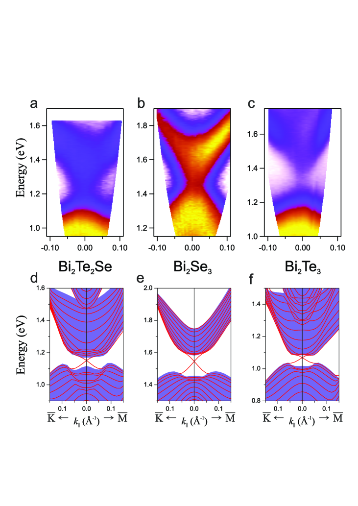
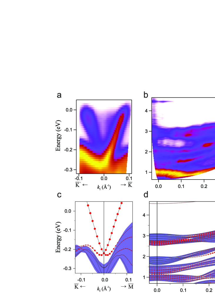
We start with the ternary tetradymite compound Bi2Te2Se which recently was shown to be a three-dimensional TI by ARPES measurements Neupane et al. (2012); Miyamoto et al. (2012). The crystal structure of this compound is obtained by replacing the central Te layer of each QL of Bi2Te3 by a Se layer. The results of photoemission experiments and DFT calculations on Bi2Te2Se are shown in Fig. 1. Shaded regions in the calculated band structure depict projected bulk bands, while red dots indicate an increased localization in the first quintuple Bi2Te2Se layer. From the ARPES data (Fig. 1(a)) the Dirac cone in the occupied part of the band structure is found eV below . Depending on crystal growth conditions values between 0.1 and 0.4 eV have been found Neupane et al. (2012); Miyamoto et al. (2012). In the 2PPE data (Fig. 1(b)) all prominent features can be attributed to unoccupied bands in the calculations (Fig. 1(d)) and we conclude that the 2PPE process is dominated by intermediate states. The measured bands of high intensity coincide well with surface resonances in the calculation, giving evidence of a high surface sensitivity. A similar degree of agreement between theory and experiment is also found for Bi2Se3 and Bi2Te3 surfaces. The present results are in qualitative agreement with the inverse photoemission spectra which show three conduction band peaks Ueda et al. (1999).
In the following we will focus on the projected bulk band gaps at energies above . Figures 2(a) and (d) show a close-up of such a gap for Bi2Te2Se. In fact both 2PPE and DFT data show that it is bridged by two linearly dispersing bands which cross at the -point. At this energy it appears in MDCs as a single spot evolving into a circle towards higher energies (see also Fig. 4(a) and sup (c)). At energies below the crossing point it turns into a surface resonance degenerate with bulk bands.
The appearance of the Dirac state in the conduction-band local gap raises the question: Is this surface state topologically protected? In contrast to the Dirac state located in the principal energy gap the new massless Dirac state is located in an local energy gap and upon going along a path between time-reversal invariant momenta (TRIMs) in the Brillouin zone the gap in the spectrum of bulk states closes and opens.
The origin of the reduction of the contribution made by extended states can be found by comparing the continuous and lattice versions of the invariant. Analysis of the relation Wang et al. (2010) of the index Fu et al. (2007) in the theory of topological insulators with the winding number does not solve the problem. It is shown in Ref. Fu and Kane (2006) that the invariant in the continuous case is alternatively expressed as
| (1) |
where is half of the Brillouin zone, and are the Berry gauge potential and the associated field strength, respectively, and is the 2M(k)-dimensional ground state multiplet. The lattice analog of Eq. (1) is Fukui and Hatsugai (2007)
| (2) |
since . in this equation are integers and due to the residual invariance Fukui and Hatsugai (2007).
From Eq. (2) we infer that the reason for cancelation of the contribution made by bulk spectrum states is the compactness of the lattice gauge theory. The existence of the second Dirac cone points out the nontrivial value of the invariant in this topologically protected state.
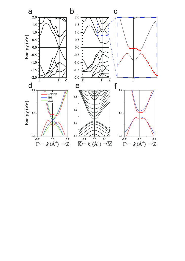
Let us consider now the bulk conduction band of Bi2Te2Se in the energy range of interest. Without spin-orbit coupling the second and third conduction bands are degenerate along the Z direction (Fig. 3(a)). Spin-orbit interaction lifts this degeneracy and opens a gap between these bands (Fig. 3(b)). Thus, the gap supporting the new “X” shaped surface state in the conduction band originates from SOI. In contrast to the principal -gap edges, which are composed of inverted Bi and Te states, both the upper and lower bands of the conduction band -gap are mostly composed of Bi states, however the Se states contribute to these bands as well. As one can see in Fig. 3(c) in the vicinity of there are two parabolic-like bands, gapped at points, where they are inverted due to the central Se atom contribution. This inversion of the local -gap edges in the conduction band along with the presence at the same energy of the gaps at F and L TRIMs of the bulk Brillouin zone (which are projected onto the point of the 2D Brillouin zone) is responsible for the emergence of the unoccupied Dirac-like surface state at Bi2Te2Se(111).
As one can see in Figs. 2(e) and (f), the FLEUR results show the topological conduction-band surface state arising in Bi2Se3 and Bi2Te3 that is fully consistent with the outcome of the experiment. The VASP vdW-DF results are almost the same: they show meV smaller unoccupied gap and slightly different position of the surface state band crossing within this gap. The arising of the unoccupied cone in Bi2Se3 and Bi2Te3, like in Bi2Te2Se, results from inversion of the QL central atom states of the SOI-induced local gap. The LDA and PBE calculations performed without taking into account the vdW forces for Bi2Te2Se and Bi2Se3 give the inverted gap too, while in the case of Bi2Te3 the SOI-induced gap is not inverted (Fig. 3(d) and Ref. sup (b)). The dissimilar character of the gap in Bi2Te3 in PBE and LDA results in absence of the unoccupied cone in the surface band structure (Fig. 3(e)). As mentioned above the different calculations were accompanied by optimization of the crystal structure. Thus, vdW-DF optimization for all systems under consideration changes and lattice parameter in the range of % and % as compared to experimental values, respectively. At the same time both the full structural optimization and the relaxation of atomic positions do not change the fractional atomic coordinates more than . To determine which factor (XC approximation or structural parameters) is more important for the change of the gap character we performed calculations of the bulk electronic structure of Bi2Te3 with two slightly different experimental parameters (Refs. Wyckoff (1964) and Nakajima (1963)) with the same exchange-correlation approximation. As one can see in Fig. 3(f) this small variation of the crystal structure changes the character of the gap. The latter means that the emergence of the unoccupied Dirac state in Bi2Te3 can be sensitive to the sample preparation. As shown in Ref. Goltsman et al. (1973) even a small deviation from the stoichiometric composition in Bi2Te3 results in the change of the lattice parameters. The data measured in the present experiment demonstrate relatively weak intensity in the cone region (Fig. 2(c)) which may be related to delicate stability of the unoccupied TSS in Bi2Te3 sample used. On the other hand the highest intensity observed for Bi2Se3 (Fig. 2(b)) reflects the more localized character of the TSS which is a consequence of the wider gap in Bi2Se3 as compared to other materials.
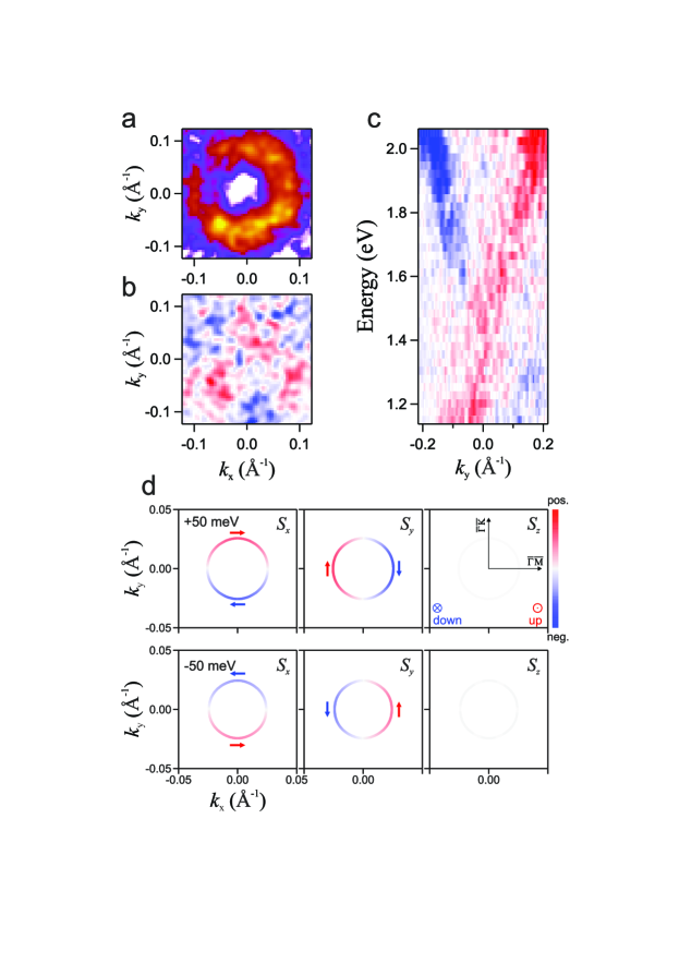
Additional evidence of the topological character of the unoccupied surface state emerges from its spin structure which can be accessed experimentally by use of CD. Therefore MDCs were recorded using left- and right-handed circularly polarized light. In Fig. 4(a) and (b) the sum + and the difference of the intensities are shown for Bi2Se3 at an energy 0.3 eV above the Dirac point. These data were obtained for a different crystal than those in Fig. 2(b) which results in a slightly different energy for the Dirac point. The normalized asymmetry covers a range of somewhat smaller than that observed by ARPES for the occupied Dirac cone where values of 30% for Bi2Se3 Park et al. (2012) and up to 40% for Bi2Te3 Jung et al. (2011); Scholz et al. have been reported. The lower asymmetry in our experiment might be attributed to the lower angular and energy resolution than in the ARPES experiments leading to an increased unpolarized background in the narrow band gap. The two transitions in 2PPE might also have opposite contributions to the CD pattern reducing the observed asymmetry. The MDCs show the expected ring and the CD pattern shows the threefold symmetry of the substrate as observed further away from the Dirac point for the occupied TSS Wang et al. (2011); Jung et al. (2011); Mirhosseini and Henk (2012) Figure 4(c) demonstrates the development of the CD pattern over a wide energy range along the direction. The dichroism is antisymmetric indicating opposite spin orientation for the two branches.
Figure 4(d) presents the calculated orientation of the electron spin within the surface state. The calculated spin-resolved constant energy contours (CECs) below and above the crossing point of the unoccupied cone state show an ideal circular shape of the CECs in agreement with present experiment and in-plane spin polarization (out-of-plane component is negligibly small) with positive (clockwise) spin helicity in the upper part and negative helicity in the lower part of the cone, i. e. the same helicity as in the Dirac cone in the principal energy gap.
In summary, we presented a study of the unoccupied part of the band structure of bismuth chalcogenides. Empty Dirac cones on Bi2Se3, Bi2Te2Se, and Bi2Te3 are identified in both DFT calculations and 2PPE experiments by their linear dispersion and helical spin structure. Their existence depends on a symmetry-inverted band gap. In the case of Bi2Te3 this inversion is sensitive to small variations of the structural parameters that can cause dependence of the empty Dirac cone in this system on sample growth conditions. The origin of the reduction of the bulk non-TRIM states contribution has been found using the invariant. The observed unoccupied TSS opens a new route to measurements on excitations in and between topological states. For TI-semiconductor junctions the unoccupied TSS might pave a way to inject and control spin-polarized currents in the semiconductor conduction band. The image-potential state seen at an energy of 4.5 eV in Fig. 1(b) corresponds to the situation discussed for magnetic monopoles Qi et al. (2009). Time-resolved photoemission experiments on image-potential states and TSSs are in progress.
Acknowledgements.
We thank Philip Hofmann for supplying additional topological insulator samples showing similar results. SVE thanks Dirk Lamoen and I. A. Nechaev for fruitful discussions.References
- Fu et al. (2007) L. Fu, C. L. Kane, and E. J. Mele, Phys. Rev. Lett. 98, 106803 (2007).
- Qi et al. (2008) X.-L. Qi, T. L. Hughes, and S.-C. Zhang, Phys. Rev. B 78, 195424 (2008).
- Zhang et al. (2009) H. Zhang, C.-X. Liu, X.-L. Qi, X. Dai, Z. Fang, and S.-C. Zhang, Nature Phys. 5, 438 (2009).
- Roushan et al. (2009) P. Roushan et al., Nature 460, 1106 (2009).
- Fu and Kane (2008) L. Fu and C. L. Kane, Phys. Rev. Lett. 100, 096407 (2008).
- Qi et al. (2009) X.-L. Qi, R. Li, J. Zang, and S.-C. Zhang, Science 323, 1184 (2009).
- Chen et al. (2009) Y. L. Chen et al., Science 325, 178 (2009).
- Hsieh et al. (2009) D. Hsieh et al., Nature 460, 1101 (2009).
- Xia et al. (2009) Y. Xia et al., Nature Phys. 5, 398 (2009).
- Yazyev et al. (2010) O. V. Yazyev, J. E. Moore, and S. G. Louie, Phys. Rev. Lett. 105, 266806 (2010).
- Eremeev et al. (2010) S. V. Eremeev, Y. M. Koroteev, and E. V. Chulkov, JETP Lett. 91, 387 (2010).
- Kuroda et al. (2010) K. Kuroda et al., Phys. Rev. Lett. 105, 076802 (2010).
- Bianchi et al. (2010) M. Bianchi, D. Guan, S. Bao, J. Mi, B. Iversen, P. King, and P. Hofmann, Nature Commun. 1, 128 (2010).
- Wang et al. (2011) Y. H. Wang, D. Hsieh, D. Pilon, L. Fu, D. R. Gardner, Y. S. Lee, and N. Gedik, Phys. Rev. Lett. 107, 207602 (2011).
- Eremeev et al. (2012) S. V. Eremeev et al., Nature Commun. 3, 635 (2012).
- Ueda et al. (1999) Y. Ueda, A. Furuta, H. Okuda, M. Nakatake, H. Sato, H. Namatame, and M. Taniguchi, J. Electron Spectrosc. Related Phenom. 101, 677 (1999).
- Sobota et al. (2012) J. A. Sobota, S. Yang, J. G. Analytis, Y. L. Chen, I. R. Fisher, P. S. Kirchmann, and Z.-X. Shen, Phys. Rev. Lett. 108, 117403 (2012).
- Boger et al. (2005) K. Boger, Th. Fauster, and M. Weinelt, New J. Phys. 7, 110 (2005).
- sup (a) See Supplemental Material at http://link.aps.org/ for details of the photoemission processes and the experimental setup.
- Rieger et al. (1983) D. Rieger, R. D. Schnell, W. Steinmann, and V. Saile, Nucl. Instr. Methods 208, 777 (1983).
- Kokh et al. (2005) K. A. Kokh, B. G. Nenashev, A. E. Kokh, and G. Y. Shvedenkov, J. Cryst. Growth 275, e2129 (2005).
- Kresse and Hafner (1993) G. Kresse and J. Hafner, Phys. Rev. B 48, 13115 (1993).
- Kresse and Furthmüller (1996) G. Kresse and J. Furthmüller, Comput. Mater. Sci. 6, 15 (1996).
- Blöchl (1994) P. E. Blöchl, Phys. Rev. B 50, 17953 (1994).
- Kresse and Joubert (1999) G. Kresse and D. Joubert, Phys. Rev. B 59, 1758 (1999).
- Perdew et al. (1996) J. P. Perdew, K. Burke, and M. Ernzerhof, Phys. Rev. Lett. 77, 3865 (1996).
- Ceperley and Alder (1980) D. M. Ceperley and B. J. Alder, Phys. Rev. Lett. 45, 566 (1980).
- Koelling and Harmon (1977) D. D. Koelling and B. N. Harmon, J. Phys. C 10, 3107 (1977).
- (29) http://www.flapw.de
- Li et al. (1990) C. Li, A. J. Freeman, H. J. F. Jansen, and C. L. Fu, Phys. Rev. B 42, 5433 (1990).
- sup (b) See Ref. sup (a) for a detailed comparison between VASP and FLEUR calculations.
- Klimeš et al. (2011) J. Klimeš, D. R. Bowler, and A. Michaelides, Phys. Rev. B 83, 195131 (2011).
- Neupane et al. (2012) M. Neupane et al., Phys. Rev. B 85, 235406 (2012).
- Miyamoto et al. (2012) K. Miyamoto et al., Phys. Rev. Lett. 109 (2012).
- sup (c) See Ref. sup (a) for momentum distribution curves from Bi2Se3.
- Wang et al. (2010) Z. Wang, X.-L. Qi, and S.-C. Zhang, New J. Phys. 12, 065007 (2010).
- Fu and Kane (2006) L. Fu and C. L. Kane, Phys. Rev. B 74, 195312 (2006).
- Fukui and Hatsugai (2007) T. Fukui and Y. Hatsugai, J. Phys. Soc. Jpn. 76, 053702 (2007).
- Wyckoff (1964) R. W. G. Wyckoff, Crystal Structures, Vol. 2. (J. Wiley and Sons, New York, 1964).
- Nakajima (1963) S. Nakajima, J. Phys. Chem. Solids 24, 479 (1963).
- Goltsman et al. (1973) B. M. Goltsman, B. A. Kudinov, and I. A. Smirnov, Thermoelectric Semiconductor Materials Based on Bi2Te3, (Army Foreign Science & Technology Center, Charlottesville VA, 1973) Report FSTC-HT-23-1782-73.
- Park et al. (2012) S. R. Park et al., Phys. Rev. Lett. 108, 046805 (2012).
- Jung et al. (2011) W. Jung et al., Phys. Rev. B 84, 245435 (2011).
- (44) M. R. Scholz, J. Sánchez-Barriga, D. Marchenko, A. Varykhalov, A. Volykhov, L. V. Yashina, and O. Rader, arXiv 1108.1053.
- Mirhosseini and Henk (2012) H. Mirhosseini and J. Henk, Phys. Rev. Lett. 109, 036803 (2012).