Zener tunneling in the electrical transport of quasi-metallic carbon nanotubes
Abstract
We study theoretically the impact of Zener tunneling on the charge-transport properties of quasi-metallic (Qm) carbon nanotubes (characterized by forbidden band gaps of few tens of meV). We also analyze the interplay between Zener tunneling and elastic scattering on defects. To this purpose we use a model based on the master equation for the density matrix, that takes into account the inter-band Zener transitions induced by the electric field (a quantum mechanical effect), the electron-defect scattering and the electron-phonon scattering. In presence of Zener tunnelling the Qm tubes support an electrical current even when the Fermi energy lies in the forbidden band gap. In absence of elastic scattering (in high quality samples), the small size of the band gap of Qm tubes enables Zener tunnelling for realistic values of the the electric field (above 1 V/m). The presence of a strong elastic scattering (in low quality samples) further decreases the values of the field required to observe Zener tunnelling. Indeed, for elastic-scattering lengths of the order of 50 nm, Zener tunnelling affects the current/voltage characteristic already in the linear regime. In other words, in quasi-metallic tubes, Zener tunneling is made more visible by defects.
I Introduction
Single-wall carbon nanotubes (SWNTs) are quasi one-dimensional wires of great interest for future electronic-devices applications. A SWNT can be constructed by rolling up a graphene sheet and its geometry is univocally specified by a pair of chiral indexes Roche . The relationship between and defines three groups of SWNTS: armchair , zigzag ( or ) and chiral nanotubes. The indexes also determine the SWNT electronic structure. If is not a multiple of 3, SWNTs of diameters in the 1-2 nm range are semiconductors with a band gap larger than 0.5 eV. Only armchair SWNTs were believed to be truly metallic. Indeed, because of the curvature, zigzag and chiral SWNTs with multiple of 3, present a small band gap of few tens of meV Min , and for this reason are called quasi-metallic (Qm) Delaney . However, recent transport measurements on chirality-identified tubes showed that also armchair tubes are Qm with to meV, likely because of electrons correlation Vikram .
The description and interpretation of the transport properties of SWNT devices, are often based on a semi-classical approach such as the Boltzmann transport equation (BTE) kane . However, the BTE can not describe some cases such us strong localization regimes Roche . Another effect that can not be described by the Boltzmann transport approach is the Zener tunneling (ZT) Zener , which is the electric-field-induced tunneling of carriers from one band to another through the forbidden energy gap . In absence of ZT, if the temperature is smaller than the gap (), only one type of carrier is responsible for charge transport: when the Fermi level, , is in the conduction (valence) band, the current is carried by electrons (holes). If is in the gap region charge-transport does not occur. On the contrary, in presence of ZT, the current is carried simultaneously by both electrons and holes and a non-zero current exists even if is in the gap region.
The critical electric field for which the ZT affects transport properties, can be estimated considering the inter-band tunneling probability across the gap of the SWNT hyperbolic bands. In absence of scattering, the transition probability as a function of the source-drain electric field is given by Andreev ; Jena where
| (1) |
and cm. is the Fermi velocity of graphene (and of Qm nanotubes far from the gap). In semiconducting tubes ( meV), V/ is unrealistically large. At experimentally-accessible electric fields, ZT is absent, and in a diffusive regime a semi-classical picture is sufficient to describe transport properties. Instead, in Qm tubes ( meV) V/, a value that nanotubes can sustain kane . In this case ZT could be observed.
In this work, we study theoretically the current voltage characteristics, of Qm nanotubes both in the linear and high field regime and we analyze the interplay between Zener tunneling and defect (or impurity) scattering. We consider long Qm tubes with an energy band gap (similar to the values measured in experiments Min ; Vikram ) in a diffusive regime, i.e. when the tube length is much longer than the defect-induced elastic scattering lengths () of 50 nm and 300 nm presently used. The approach is based on the solution of the master equation for the evolution of the density matrix. This approach correctly describes inter-band Zener tunneling.
II General assumptions
We take into account the elastic scattering of electrons with defects (we consider scattering of electrons by short-range potential) and the inelastic scattering with optical phonons. We do not consider the possible occurence of weak or strong localization effects Roche . Elastic and phonon scattering are assumed to be incoherent and, thus, the phase coherence length . Scattering with acoustic phonons plays a minor role since it is characterized by scattering lengths that are much larger than the used here (see e.g. Ref. bushmaker09, ). We suppose that the tubes are supported and that, for the regime under study, the phonon population is equilibrated at the temperature of the substrate. We assume that the doping and the potential drop is uniform along the channel, and that the electron population of the valence and conduction bands is independent on the position in the channel. Namely, we consider the bulk transport properties of an infinite SWNT under a spatially homogeneous electric-field applied along the tube axis.
We remind that at high bias conditions in small gap nanotubes, the scattering with optical phonons can lead to a current saturation kane and to nonequilibrium optical-phonon population (hot phonons) Lazzeri1 ; Lazzeri2 . In suspended metallic tubes, this can lead to the observation of negative differential resistance pop05 ; bushmaker09 . This kind of phenomena are not included in the present model and their inclusion would lead to increase of the differential resistance for high electric field (this point will be discussed in Sects. IV- V.2).
Electronic transport measurements in Qm nanotubes were reported in Vikram, ; bushmaker09, . The two papers deal with transport regimes which are quite differents from the present one. Because of this, the results of Vikram, ; bushmaker09, can not be directly compared with the present ones. In particular, in both Vikram, ; bushmaker09, , the elastic scattering lengths are much longer than in the present work and, in both cases, they are comparable with the length of the tubes. Because of this, Ref. Vikram, can observe interference effects between the contacts and Ref. bushmaker09, can interpret the results by assuming an electronic distribution non uniform along the length of the channel. On the contrary, in the present work we are in a diffusive regime: the scattering length , where is the length of the tube, and , where is the phase coherence length. In this diffusive regime, we can assume a uniform distribution of the electrons along the tube and that interference effects between the contacts are not observable.
III Density matrix in an uniform electric field
III.1 Hamiltonian
The graphene Hamiltonian for the -bands close to the point (Dirac point) of the Brillouin zone (BZ) is Castro :
| (2) |
where is the Fermi velocity, with and the Pauli matrices. is the momentum operator in the two-dimensional BZ of graphene. is a 22 matrix which describes the and bands. Starting from Eq.(2), one can derive an effective Hamiltonian for a SWNT:
| (3) |
is the momentum operator in the one-dimensional BZ of the nanotube (a momentum parallel to the tube axis) and is a constant fixed by the energy Gap . The eigenstates of are Bloch states and have the form
| (4) |
Here is the length of the system and , is the periodic part of the Bloch state:
| (5) |
where . indicates positive energy (conduction band) whereas describes states with negative energy (valence band) with respect to the Dirac point. The eigenvalues of read:
| (6) |
We now apply a spatially homogeneous and static (source-drain) electric field along the tube axis. The Hamiltonian, in the vector-potential gauge, becomes :
| (7) |
Where is the vector potential component along the tube axis, and the electron charge. The instantaneous eigenstates of the time dependent Hamiltonian, Eq.(7), are given by krieger1 :
| (8) |
with eigenvalues .
III.2 High field: non-linear regime
A framework in which quantum effects such as Zener tunneling appear naturally is the Liouville-Von Neumann Master Equation (ME) Rossi . Within this formalism our variable is the one-electron density-matrix operator . The time evolution of in absence of scattering processes is given by:
| (9) |
Since we are dealing with a spatially homogeneous electric field applied to an infinite nanotube, only the elements of the density matrix diagonal with respect to will be relevant Rossi2 . We use the instantaneous eigenstates (Eq.(8)) as basis. Then, from Eq.(9) one finds the time evolution of krieger2 :
| (10) |
where and is defined by:
| (11) |
The term introduces the inter-band transitions. Using perturbation theory for the derivative with respect to we can show that:
| (12) |
where is the velocity operator defined by:
| (13) |
For our system takes the form:
| (14) |
The full evolution equation is obtained by adding the collision integral to the right-hand side of Eq.(10). The collision integral results from the sum of two independent contributions due to inelastic electron-phonon scattering and elastic electron-defect scattering. Electron-phonon scattering is treated as in Ref. graham and read:
| (15) |
where , the electron-phonon scattering probability is evaluated using Fermi golden rule Hamaguchi :
| (16) |
with the coupling matrix
elements and the phonon branch. is the
phonon energy with and is the
phonon population. The upper (lower) sign in the delta function
corresponds to phonon emission (absorption).
The elastic scattering by defects is supposed to be incoherent. In this case the collision integrals for the diagonal and non-diagonal elements of the density matrix are given by:
| (17) |
| (18) |
The transition probability, within the Fermi golden rule, is defined by :
| (19) |
Where is the density of defects (that is the number of defects per unit length) and is the scattering potential.
Finally, the master equation, that describes the time evolution reads:
| (20) |
For a given value of the electric field , a steady-state solution of Eq.(20) is reached for . In this work, the steady-solution is obtained by numerical integration in time using a finite-difference method.
The electronic population (that is the diagonal elements ) determines the density of electrons (number of electrons in excess per unit length of the tube) by:
| (21) |
where and are respectively the spin and valley degeneracy. is a constant of motion of Eq.(20). We will show simulations done at different values of the Fermi level , that is by fixing the initial value of to:
| (22) |
Where is the Fermi-Dirac function, computed here for K.
The charge current is given by :
| (23) |
where is defined by :
| (24) |
Using the definition of the velocity operator given in Eq.(13), one can show that
| (25) |
Finally the steady current will be evaluated for the steady-state solution.
An interesting aspect of the master equation, is that we can recover the standard Boltzmann transport equation (BTE), i.e. the semiclassical description, setting of Eq.(20) to zero. In this case the diagonal elements of the density matrix evolve according to:
| (26) |
and the off-diagonal elements of the steady solution vanish.
III.3 Linear regime
In this section, we derive a set of simplified equations (which can be evaluated analytically) valid for small values of the electric field within the linear regime. In the linear regime the applied field will cause a small deviation of the equilibrium distribution . The steady state density matrix (with ) can be written as:
| (27) |
where is the density matrix element in absence of field and the deviation linear in . is the equilibrium distribution which is diagonal and equal to . Inserting Eq.(27) in Eq.(20), and keeping all the terms linear in , one obtains the solution for the diagonal elements of the density matrix:
| (28) |
with , the momentum relaxation time, defined by Hamaguchi :
| (29) |
where for back-scattering processes and for forward scattering ones. Indeed, after the scattering with a defect (or a phonon), the electron can either maintain its propagation direction, which is forward scattering (fs), or reverse it, which is back-scattering (bs). The off-diagonal elements are given by:
| (30) |
where is defined by :
| (31) |
where , and , are respectively the elastic, hole-phonon and electron-phonon scattering rate for the equilibrium distribution and defined by:
| (32) |
| (33) |
| (34) |
III.4 Zero-field electrical conductivity
The zero-field conductivity, , can be obtained by inserting the steady state solutions of the linear regime, Eqs.(28) and (30) in the current expression, Eq.(23):
| (35) |
where is the conductivity obtained from the diagonal elements of the density matrix. It is given by:
| (36) |
is the semi-classical conductivity of the Boltzmann equation and at zero temperature it reduces to:
| (37) |
with the Fermi momentum and the one-dimensional density of states (DOS) per unit length. For the lowest sub-band of the Qm nanotube Lundstrom :
| (38) |
where is the constant DOS (per unit length) of the lowest sub-band of a metallic tube. is the step function which equals 1 for and otherwise. In the case of a metallic tube the conductivity, Eq.(37), can be written as:
| (39) |
where , the elastic scattering length, is given by:
| (40) |
The current due to Zener inter-band is given by , that arises from the off-diagonal part of the density matrix, Eq. (30):
| (41) | |||||
Notice that this expression is similar to the off-diagonal Kubo formula for the optical conductivity Nomura but with a finite value of the parameter . When , the Zener contribution () vanishes and the total conductivity is equal to that of the semiclassical Boltzmann approach (). Thus, in the linear regime, the Zener tunnelling contributes to the transport only in presence of scattering events that limit the carrier lifetime. On the contrary, at finite field, Zener tunneling can occur in the ballistic case (see formula right above Eq.(1)).
IV Transport calculations
We performed calculations for a metallic tube and a quasi-metallic tube (Qm) with an energy band gap (similar to the values measured in experiments Min ; Vikram ). The tubes are subject to a spatially uniform electric field and the number of carriers (electrons or holes) is varied by changing the Fermi level . In the metallic tube the dispersion relation is linear , with , in a Qm tube the bands are hyperbolas, Eq.(6).
The transport properties of the Qm nanotube are explored by a semi-classical and a quantum-mechanical approach. In the semi-classical case, we do not take into account the inter-band transitions due to the electric field by setting to zero the off-diagonal elements of the density matrix ( with ). The evolution of the system is then governed by the BTE, Eq. (26). In the quantum approach, we take into account the inter-band transitions due to the electric field by considering the off-diagonal elements of the density matrix. The evolution is then governed by the ME, Eq. (20).
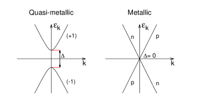
For the metallic tube, the ME that governs the quantum evolution can be obtained in the limit . In this case, the coupling [(Eq. (11)], that promotes Zener transitions, diverges at , and the electrons that cross the point tunnel with 100% probability from the valence (conduction) to the conduction (valence) band. As a consequence, for metallic tubes, the quantum-mechanical approach (ME) reduces to the semiclassical approach (BTE) if we change the meaning of the band indexes in Eq. 26. In particular, while for Qm tubes we distinguish between “valence” and “conduction” bands, for metallic tubes we distinguish between bands with positive or negative velocity ( or ), see Fig.1.
We consider short-range scatterers and the electron-defect coupling is taken to be a constant and -independent. Under this hypothesis in a metallic tube the elastic scattering mean free path is -independent. The value of is determined fixing nm and nm. In the Qm tubes, is also assumed to be a constant equal to that of the metallic tubes. Note, however, that, in the Qm case, the scattering mean free path become -dependent. Indeed, because the presence of a gap, the density of states, that determines the scattering rate, is energy dependent.
Only three optical phonons can play an important role in transport phenomena at high bias: two (longitudinal and transverse) correspond to the graphene optical phonons at with symmetry E2g, and one corresponds to the graphene phonon at with symmetry A kane ; Euen ; Lazzeri1 ; Lazzeri2 . The energies of these phonons are respectively and . For our calculation the electron-phonon coupling matrix elements are taken constant and independent of and , with . The label stands for a back-scattering process (), and stands for a forward scattering process (). In a metallic tube, the corresponding scattering lengths, , are proportional to the tube diameter Lazzeri2 , that we assume to be 2 nm. In this case, nm, nm and . For the Qm tubes we use the obtained in the metallic case. The phonon population is set to zero (cold phonons, only phonon emission is treated). We do not consider the generation of hot phonons, that occurs at high bias in nanotubes, when the elastic scattering length is much larger than the phonon one, Lazzeri2 . In the present case, this is justified by the strong elastic scattering used in the present model that competes with the phonon scattering, as in graphene Amelia .
V Results and discussion
We now show the results obtained for two different values of the elastic scattering length, namely nm and nm. The goal is to understand in which conditions the Zener tunneling is experimentally observable. We will compare the results obtained with the semi-classical (or Boltzmann) approach with those obtained with the quantum treatment (master equation). In the semi-classical approach the Zener tunneling is not allowed. Thus, the semi-classical and quantum results will differ when Zener tunneling is relevant. Results for metallic tubes (for which the distinction quantum versus. semi-classical does not hold) are shown as a comparison. The results shown for a finite value of the source-drain electric field, , are obtained from numerical solution of the transport equations. The results for are derived analytically in Sec. III.4
V.1 Conductivity and current as a function of the Fermi energy
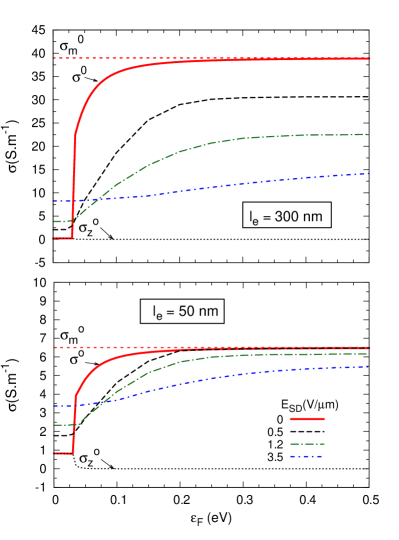
Fig. 2 reports the conductivity of the Qm tube as a function of the Fermi level for various values of the electric field . In Fig. 2, is the zero-bias () conductivity calculated in the linear regime for the temperature K. is the component of due to Zener tunneling ( is a well defined quantity, see Sec. III.4), and is the zero-bias conductivity of a metallic tube.
For the metallic tube, the conductivity has a finite value which is proportional to the elastic scattering length and which does not depend on (this is true as soon as does not meet the higher subbands of the SWNT, which are not considered in this study). For the Qm tube, the conductivity tends to be equal to the metallic one for : when the doping is sufficiently high there is only one type of carriers, the details of the electronic bands near the Dirac point are not relevant, the transport is properly described by the semi-classical Boltzmann approach and the Qm and metallic tube behavior are indistinguishable. On the other hand, for the presence of the electronic gap acts as a barrier and the Qm conductivity suddenly diminishes. In particular, from Fig. 2, for , meaning that the Qm conductivity is entirely due to Zener tunneling (inter-band) and that the Boltzmann conductivity (intra-band) vanishes. Fig. 2 also reports the finite field conductivity for different values of the electric field. Also at finite field, the conductivity is entirely due to Zener tunneling for small values of .
The comparison of the results obtained for different values of the elastic scattering lengths, , is very remarkable. Indeed, for small doping (), the zero-bias conductivity for the smallest scattering length ( S.m-1 for nm in Fig. 2), is higher than the one for the longest scattering length, ( S.m-1 for nm). Moreover, most important, the ratio between the high doping (0.2 eV) and the small doping is much higher for the smallest scattering length than for the longest one.
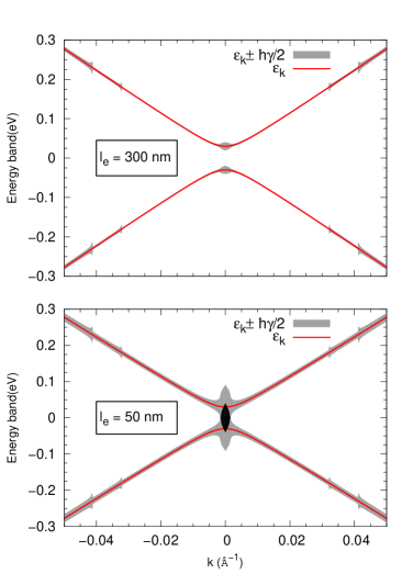
This counterintuitive behavior can be understood by considering the electronic scattering rate (or broadening) , defined in Eq. 31. represents the uncertainty with which the energy of an electronic band can be defined. Fig. 3 reports the electronic bands for the Qm tube: the bands are represented as lines with a finite thickness (gray area in Fig. 3) equal to . The increased value of in the vicinity of the gap is due to the elastic scattering. The broadened electronic bands of Fig. 3 overlap near for nm (low quality samples), meaning that, because of energy-uncertainty, the electrons do not see the gap and can tunnel from a band to the other even if the applied field is small. On the contrary, for nm (better quality samples) the bands do not overlap and for small electric field the Zener tunneling can not take place. In Fig. 3, the sudden increase of the broadening for Å-1 is due to the scattering with optical phonons. This scattering mechanism is active only when and , which is far from the gap. Zener tunneling is, thus, activated only by the elastic scattering (with defects) and not by the scattering with optical phonons.
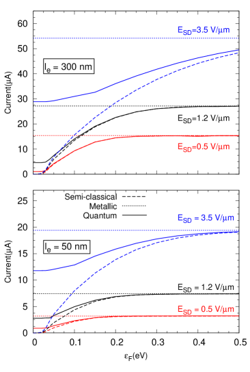
Finally, to see the things from a different perspective, Fig. 4 reports the current as a function of for various values of the electric field . For large doping (large ), the Qm tube current calculated with the semiclassical and with the quantum approaches tend to be equal. Also, both currents tend to be equal to the metallic tube one. The semi-classical approach predicts a zero current in the gap and underestimates the current in a range of that increases with . In the region of the gap, the current is thus entirely due to Zener tunneling.
V.2 Current as a function of the electric field
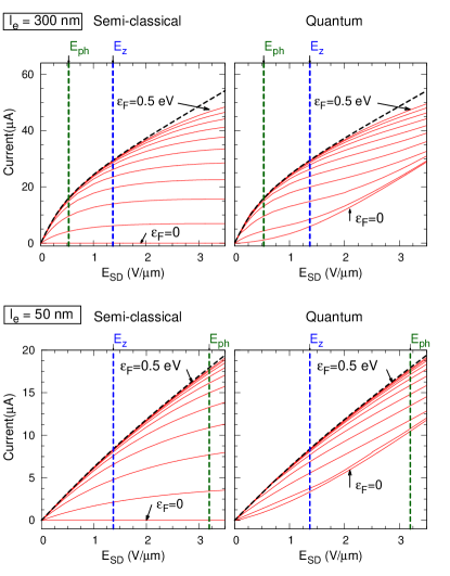
To analyze the results as a function of the electric field , we consider two characteristic fields: and . is defined in Eq. (1) and it is the value of the electric field for which, in the absence of scattering, the Zener scattering is expected to be sizable. is defined as and it is the value of the field for which optical-phonon emission become sizable compared to elastic scattering. is higher for smaller values of . To understand this definition, one should consider that optical phonons have a finite energy . In order to emit an optical phonon an electronic carrier needs to attain a minimum activation energy corresponding to . This is possible if the carrier has accelerated in the electric field at least through a length kane . The process is dominated by the zone boundary phonons since . For small electric fields, , and the scattering with defects prevents the carriers to accelerate and, thus, to reach the activation energy. On the other hand, if , and the carriers can attain the activation energy before scattering with the defects. Thus, for small electric field, elastic scattering is the dominant scattering mechanism (in this regime the current-voltage curve of metallic tubes is linear kane ). For electric fields higher that the scattering with optical phonons is activated. This is associated with a decrease of the differential conductivity (sub-linear current-voltage curve) which can lead to a saturation of the current at high drain-source voltages in metallic tubes with long elastic scattering lengths kane . The scattering with optical phonons can lead to an anomalous increase of the optical-phonon population (hot-phonons) Lazzeri1 ; Lazzeri2 which, in turn, will further diminish the high-bias conductivity.
Fig. 5 shows the current as a function of the electric field for different values of . At high doping, the results for the semi-classical (BTE) and of the quantum (ME) approaches are very similar and approach the metallic results. The two approaches provide significantly different results for sufficiently high electric fields and small values of the Fermi level. In particular, for the current is exactly zero within the semi-classical model, while the current has a finite value, which increases with the electric field, within the quantum approach, Fig. 5. For and eV, within the quantum approach the current versus. electric field is a super-linear curve for . Such a behavior was observed in graphene Niels and in large diameter nanotubes Anantram , and identified as due to Zener tunneling.
Let us compare the results for the different scattering lengths (Fig. 5). Zener tunneling should be more visible for 50 nm, than for 300 nm, for two reasons. First, for 50 nm, the Zener current is already relevant for electric fields smaller than (this is explained in the discussion related to Fig. 3). Second, for 50 nm , while for 300 nm . Now, the scattering with optical phonons is associated to a sub-linear current which tend to mask the presence of the super-linear Zener current. For 50 nm, means that this “masking” does not occur in the region of interest. For 300 nm, means that this “masking” is already active in the region where Zener is active. Beside this, one should also consider that in the present simulations we are not including the possibility of hot phonons. The inclusion of this effect would decrease the differential conductance for . This should not change the 50 nm curves but should further mask the Zener current in the 300 nm case.
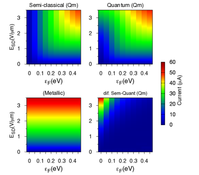
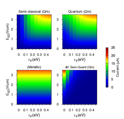
Finally, in by Fig.7 and 7 we present the two-dimensional maps of the current as a function of and . In one of the panels, we also report the difference between the current obtained within the quantum approach and that of the semi-classical calculation. This difference is higher where the Zener tunneling is more important. For metallic tubes, the current does not depend on the Fermi level because, within the linear band approximation, the electronic density of states is a constant. Note that for sufficiently high values the semi-classical and the quantum results for the Qm tubes are almost indistinguishable and approach the results for the metallic tubes.
V.3 Steady-state distribution functions
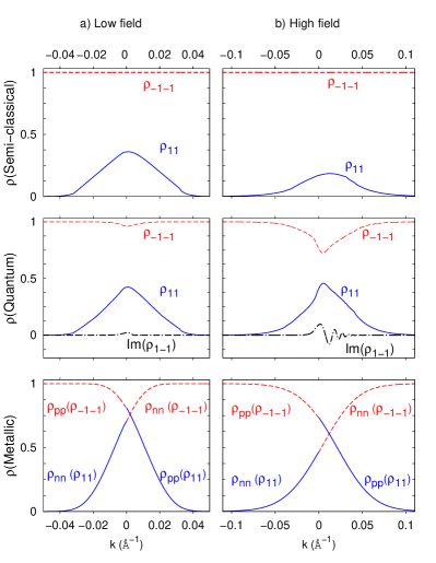
It is instructive to compare the steady-state distribution functions of the electronic populations associated with the semi-classical or quantum approaches. Fig. 8 reports the distribution functions obtained for nm and the Fermi level eV, that is for conditions in which the quantum effects are relevant. In Qm tubes, when the quantum approach is used both electron and hole contribute to the current, whereas in the semiclassical approach only electrons carry a current since the valence band is filled. Interestingly, at high field the population of Qm tubes tends to that of metallic tubes only when the quantum approach is used. Indeed, in the metallic tube (which corresponds to the limit ) the tunneling between valence and conduction band is total. The metallic limit can be reached only when one includes interband transitions. Fig. 8 also shows the imaginary part of the off-diagonal element of the density matrix . This quantity is different from zero when quantum effects are relevant. One can remark that Zener tunneling turns on near (with a maximum at ) and decays after few oscillations for . The typical wave vector associated with these oscillations is , being the electronic gap.
VI Conclusion
We have presented a theoretical model based on the master equation to explore the quantum effects (inter-band transitions induced by electric field or Zener tunneling) on the transport properties of homogeneous quasi-metallic carbon nanotubes (Qm). The presence and relevance of the Zener tunneling has been highlighted by comparing with a semi-classical Boltzmann transport approach, in which the inter-band transitions are neglected. We studied Qm tube with an electronic gap meV in the presence of impurities or defects which influence the transport by providing an elastic scattering channel for the carriers. Zener tunneling is relevant for small doping, when the Fermi energy lies in or close to the forbidden gap . In absence of elastic scattering (in high quality samples), the small size of the band gap of Qm tubes enables Zener tunnelling for realistic values of the the electric field (above 1 V/m). However, for such electric fields the scattering with the optical phonons (whose effect is underestimated in the present approach) tends to mask the Zener current. On the other hand, the presence of a strong elastic scattering (in low quality samples) further decreases the values of the field required to observe Zener tunnelling. Indeed, for elastic-scattering lengths of the order of 50 nm, Zener tunnelling affects the current/voltage characteristic already in the linear regime. In other words, Zener tunneling is made visible by defects in Qm tubes. This result is similar to what has been recently shown for graphene Niels .
Calculations were done at IDRIS, Orsay, project 096128.
References
- (1) Jean-Christophe Charlier, Xavier Blase and Stephan Roche, Rev. Mod. Phys., Volume , ( 2007)
- (2) M. Ouyang, J-L. Huang, C. L. Cheung, and C. M. Lieber, Science , 702 (2001)
- (3) P. Delaney, H. J. Choi, J. Ihm, S. G. Louie, M. L. Cohen, Nature , 466 (1998).
- (4) V V. Deshpande, B. Chandra, R. Caldwell, D S. Novikov, J. Hone and M. Bockrath, Science vol. , 106 (2009).
- (5) Z. Yao, C L. Kane and C. Dekker, Phys. Rev. Lett. , 2941 (2000).
- (6) C. Zener, Proc. Roy. Soc. (London) , 523 (1934).
- (7) A. V. Andreev, Phys. Rev. Lett. , 247204 (2007).
- (8) D. Jena, T. Fang, Q. Zhang, and H. Xing, Appl. Phys. Lett. , 112106 (2008).
- (9) A.W. Bushmaker, V.V. Deshpande, S. Hsieh, M.B. Bockrath, and S.B. Cronin, Nano Lett. 9, 2862 (2009).
- (10) M. Lazzeri, S. Piscanec, F. Mauri, A. C. Ferrari, and J. Robertson, Phys. Rev. Lett. , 236802 (2005).
- (11) M. Lazzeri, F. Mauri, Phys. Rev. B. , 165419 (2006).
- (12) E. Pop, D. Mann, J. Cao, Q. Wang, K. Goodson, and H. Dai, Phys. Rev. Lett. 95, 155505 (2005).
- (13) Castro Neto A. H., Guinea F., Peres N. M. R., Novoselov K. S. and Geim A. K., Rev. Mod. Phys. , 109 (2009)
- (14) J. B. Krieger and G. J. Iafrate, Phys. Rev. B , 5494 (1986).
- (15) Fausto Rossi, Theory of Semiconductor Quantum Devices, Springer, 2011.
- (16) Fausto Rossi and Tilmann Kuhn, Rev. Mod. Phys. , (2002).
- (17) J. B. Krieger and G. J. Iafrate, Phys. Rev. B , 9644 (1987).
- (18) R. Hübner and R. Graham, Phys. Rev. B , 4870 (1996).
- (19) Chihiro Hamaguchi, Basic Semiconductor Physics, Springer Berlin Heidelberg, 2010.
- (20) Mark Lundstrom and Jing Guo Nanoscale Transistors, Springer-verlag, 2006.
- (21) Kentaro Nomura and A. H. MacDonald, Phys. Rev. Lett 076602 (2007)
- (22) J-Y. Park, S. Rosenblatt, Y. Yaish, V. Sazonova, H. Üstunel, S. Braig, T. A. Arias, P. W. Brouwer, and P. L. McEuen, Nano. Lett. , 517 (2003).
- (23) A. Barreiro, M. Lazzeri, J. Moser, F. Mauri, and A. Bachtold, Phys. Rev. Lett. , 076601 (2009).
- (24) N. Vandecasteele, A. Barreiro, M. Lazzeri, A. Bachtold, and F. Mauri, Phys. Rev. B , 045416 (2010).
- (25) A. Svizhenko, M. P. Anantram, and T. R. Govindan, IEEE Trans. Nanotechnol. , (September 2005), 557-562.