Effects of interface resistance asymmetry on local and non-local magnetoresistance structures
Abstract
Spin injection and detection are very sensitive to the interface properties between ferromagnet and semiconductor. Because the interface properties such as a tunneling resistance can be chosen independently between the injection and detection sides, the magnetic transport properties are considered to depend on the asymmetry of the two interfaces. We theoretically investigate the effect of the asymmetric interfaces of the injection side and the detection side on both the local and non-local magnetoresistance measurements. The results show the magnetoresistance ratio of local measurement structure has its maximum at the symmetric structure, and the effect of the asymmetry is very weak for the non-local measurement structure.
I Introduction
Since the successful detection of spin accumulation signals in Si at room temperature (RT), electrical spin injection and detection in semiconductors (SC) have been actively studied Appelbaum ; Dash ; Suzuki ; Li ; Jeon ; Ando ; Vera-Marun ; Vera-Marun2 ; InokuchiJAP ; Ishikawa ; Saito1 ; Jansen ; Uemura for realizing spin-based MOSFETs Tanaka ; Saito2 ; Saito3 ; Tanamoto .Up to now, spin injection and detection in Si have been achieved using hot-electron transport Appelbaum , or spin-polarized tunneling Dash ; Suzuki ; Li ; Jeon . The electrical creation and detection of spin accumulation in n-type and p-type Si were recently demonstrated using FM/tunnel contacts Dash ; Suzuki ; Jeon and FM/Schottky-tunnel-barrier contacts Ando up to RT. Recently, we have also succeeded in observing spin accumulation signals at RT by using epitaxially formed CoFe/AlOx InokuchiJAP ; Saito1 and CoFe/MgO Ishikawa ; Saito1 electrodes on Si-on-insulator substrates with Si (100) surfaces. In the case of CoFe/MgO electrodes, we have observed relatively large spin accumulation signals with relatively long spin relaxation times ( ns) at RT Ishikawa ; Saito1 . For ferromagnet (FM)/SC systems, in general, spin injection and detection efficiencies strongly depend on the spin polarization of the used FM electrode, the interfacial quality, and the interface resistance between FM and SC. In particular, insertion of an interface resistance using a tunnel barrier between FM and SC is a promising method for demonstrating highly efficient spin injection and detection Schmidt ; Rashba ; Fert2001 . These indicate that it is better that the interface resistance of the injection side should be sufficiently high in order to solve the issue of conductance mismatch between the FM and the SC. Regarding the detection side, in order to prevent the refection of spin-polarized electron at the interface Fert2001 , low interface resistance region might be better. Then, there arise questions such as (1) whether the injection resistance should be larger than detection resistance and (2) Is there any different correlation about the interface resistance asymmetry between local magnetoresistance (MR) setup and non-local MR setup?
Here we theoretically study the effects of the interface resistance asymmetry between FM and nonmagnetic conductor (N) on the MR in both local MR setup (Fig.1(a)) and non-local MR setup (Fig.1(b)). Because both the spin injection and detection affect the spin-dependent transport properties, the symmetry of the device structure is considered to play an important role for the MR ratio. We extend the standard theories by Fert et al. Fert2001 for the local MR measurement and Jedema et al. Jedema2 for the non-local MR measurement, and derive the analytical formula for the asymmetric interface resistances.
In §2, formulation of our model is presented. Section 3 is devoted to the analytical and numerical calculations and discussions for the local measurement setup. The non-local MR measurement setup is investigated in §4. Finally, the conclusions are given in §5. We expect that these novel results will open a pathway for development of next-generation spin transistors.
II Formulation
The spin accumulation effect, the difference between the chemical potential of the up spin and that of down spin is described by the diffusion equations Fert2001 ; ValetFert ; Jaffres ; Fert2012 ; Jedema2 . The relationship between the spin current density and () is given by where is a spin-dependent conductivity. The diffusion equation for the chemical potential is given by
| (1) |
where
| (2) |
is an average spin diffusion length for region () and region (). The boundary conditions at the interface () are (1) spin current is continuous and (2) the chemical potential is continuous at the interface such as . We also write and for the resistivity of the ferromagnet and the nonmagnet . The important quantities here are and . We consider the spin-dependent interface resistances (injection side) and (detection side) for a unit surface described by
| (3) | |||||
| (4) |
III Local measurement setup
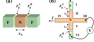
Here we consider the effect of the asymmetric structure on the local measurement setup (Fig.1(a)). In this case, Fert et al.Fert2001 showed that there is an appropriate interface resistance condition of the injection side in which the MR ratio has a peak when there is an impedance matching . However, because they assume the symmetric structure, it was unclear the appropriate condition at the detection side. Thus we focus on the effect of the asymmetry of the device structure on the MR ratio.
Following Ref.Fert2001 , we assume the solutions of the diffusion equations for the left, middle and right electrodes. For example, and , where and are a bulk spin asymmetry coefficient and the current that flows through the system, respectively. () is an unknown coefficient to be determined by the boundary conditions. By the same procedure as that of Ref. Fert2001 , we obtain the resistance of anitiparallel (AP) configuration, , and that of parallel (P) configuration, . The resistance change for Fig.1(a) is given by
| (5) |
where
| (6) | |||||
Similarly, for a multilayer structure as Ref.Fert2001 , we obtain
| (7) |
where
| (8) | |||||
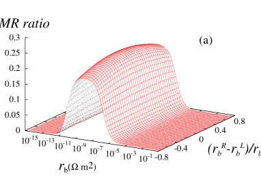
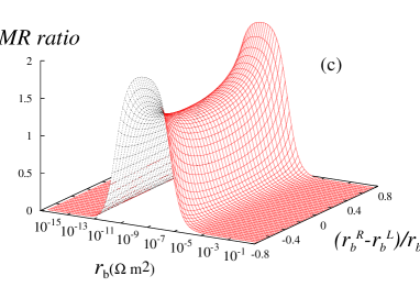
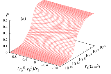
In Eqs.(7) and (8), we assume that thickness of is much larger than as in Ref.Fert2001 . The MR ratio is defined by . Fig.2 shows the numerical result of Eq.(7) as a function of and for the case of ((a) and (b)) and that in which and change as and ((c)). For (Fig.2 (a)(b)), the MR ratio has its maximum when interface resistance is symmetric (). We can also see that the effect of the asymmetry on the MR ratio is not large as long as the difference between and is not large. Thus we can say that the impedance matching condition is also satisfied at the detection side. Fig.2 (c) shows the case that and change with and . It can be found that the MR ratio increases as the asymmetry increases. Note that the minimum structure at the symmetric point can be seen at . Thus, this result says that the strong interface asymmetry coefficient changes the magnetic properties of the system.
Let us consider the effect of the asymmetry around the symmetric point analytically based on Eqs.(6) and (7). We consider the impedance matching region in which . Then can be neglected. In this region Eqs.(6) and (7) have the same form given by
| (9) |
where
| (10) | |||||
| (11) |
assuming and . In particular, when , we have
| (12) |
Thus, has its maximum value at its symmetric point ().

IV Non-local measurement setup
Here we consider the effect of the asymmetric structure on the non-local measurement setup (Fig.1(b)). Jedema et al. Jedema2 showed the case of no interface resistances in Fig.1(b). In case of the non-local measurement setup, we can also introduce the asymmetry of and . We can also investigate the effect of distance between the voltage part and the current part. Here, the diffusion equations that we use here are the same as those in Ref. Jedema2 :
| (13) | |||||
| (14) | |||||
| (15) | |||||
| (16) | |||||
| (17) | |||||
| (18) |
where , , , , , , , and are unknown constants that are determined by boundary conditions. Regions (I) and (VI) in Fig.1(b) correspond to the injection and detection ferromagnetic contacts, respectively. Regions (II)-(V) correspond to the intermediate semiconductor regions. The electric current flows from the region (I) to the region (IV). In regions (III) and (V), spin polarized current flows while the electric current does not flow. Although in the general non-local measurement, there is a finite distance between the region (II)-(IV) and the region (III)-(V), as long as we consider the magnetic properties, the interface between the semiconductor and the ferromagnetic contacts play the intrinsic role. Therefore we apply the cross structure depicted in Fig.1(b).
The resistance change, , where is the cross-sectional area of the nonmagnetic strip, is obtained by
| (19) |
where , , , , , and
| (20) | |||||
| (21) |
with . For the symmetric case, this equation is reduced to that of Ref. Jedema2 .
The spin current polarization at the interface of the current injecting contact is given by and we have
| (22) |
When , this result coincides with Eq.(15) in Ref.Jedema2 .
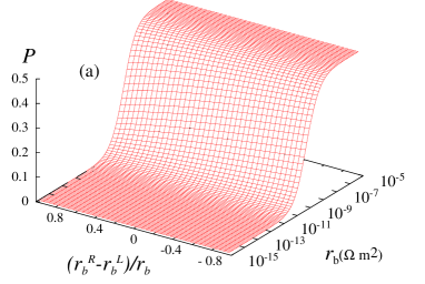
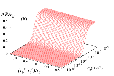
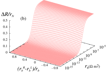
Fig.3 shows the calculated ((a)) and ((b)). Compared with Ref.Jedema2 , we can see that the interface resistance Eq.(4) enhances and such that and are saturated as increases Fukuma . As can be seen from these figures, the effect of the asymmetry of the left and the right tunneling seems to be small. Now let us analyze the and around their symmetric point. Because Eq.(19) is symmetric regarding the and , it is easily inferred that the symmetric point will correspond to a maximum or minimum point similar to the local measurement case (Fig.1(a)) when . Because , we can neglect in Eq.(19). By using Eqs.(10) and (11), for , we have
| (23) |
When
| (24) |
These quantities have their maximum values at and . Thus, the MR is found to have their maximum at the symmetric point. Similarly when , we have
| (25) | |||||
Thus, in this region, as decreases ( decreases) and increases ( increases), increases. However, because , the absolute value of is small such as . When
| (26) |
Thus, for , is determined only by . The effect of the asymmetry can be neglected in this region. Thus, in contrast with the local measurement setup, we can see the effect of asymmetry only in the region .
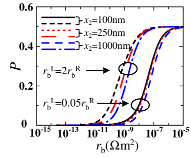
Next we investigate in what region the asymmetry affects the spin polarized current. Fig.4 shows for when changes. We can see that the large asymmetry shifts the impedance matching points. In addition, for () is better than that for (). This result shows that, as noted in the Introduction, low interface resistance is better in the detection side (). Fig.5 (a) shows the results when the length of the nonmagnet is as short as the spin diffusion length such as nm and nm. We can see that the effect of the asymmetry becomes remarkable for . This is because the distance between the left and the right junctions is small and the effect of the two junctions is sufficiently strong. On the contrary, the resistance change (Fig.5 (b)) again does not strongly depend on the interface asymmetry.
V Conclusions
We studied the effects of the interface asymmetry between ferromagnet and nonmagnet on the spin-dependent transport properties for both the local and non-local measurement setups, based on diffusion equations. We showed that the MR ratio has its maximum value at the symmetric structure of the conventional case of for the local measurement setup. For the non-local measurement setup, both the resistance change and the spin current polarization monotonically increase and saturate as the interface resistance increases, even if there is the interface asymmetry. In particular the resistance change and the spin current polarization is affected by the interface asymmetry only below the impedance matching region. We can conclude that, as long as the asymmetry is not large, spin-dependent transport properties are not strongly affected by the asymmetry of the interface resistance for the non-local measurement setups.
Acknowledgements.
We thank A. Nishiyama, J. Koga and S. Fujita for useful discussions.References
- (1) I. Appelbaum, B. Huang, and D.J. Monsma: Nature (London) 447 (2007) 295.
- (2) S.P. Dash, S. Sharma, R.S. Patel, M.P. Jong, and R. Jansen: Nature (London) 462 (2009)491.
- (3) T. Suzuki, T. Sasaki, T. Oikawa, M. Shiraishi, Y. Suzuki, and K. Noguchi: Appl. Phys. Express 4 (2011) 023003.
- (4) C.H. Li, O.M. J. van’t Erve, and B.T. Jonker: Nature Commun. 2 (2011) 245.
- (5) K.R. Jeon, B.C. Min, I.J. Shin, C.Y. Park, H.S. Lee, Y.H. Jo, and S.C. Shin: Appl. Phys. Lett. 98 (2011) 262102.
- (6) Y. Ando, K. Kasahara, S. Yamada, Y. Maeda, K. Masaki, Y. Hoshi, K. Sawano, M. Miyao, and K. Hamaya: Phys. Rev. B 85 (2012) 035320.
- (7) I. J. Vera-Marun, V. Ranjan, and B. J. van Wees: Nature Phys. 8 (2012) 313.
- (8) M. H. D. Guimaraes, A. Veligura, P. J. Zomer, T. Maassen, I. J. Vera-Marun, N. Tombros, and B. J. van Wees: Nano Lett. Article ASAP, DOI 10.1021/nl301050a
- (9) T. Inokuchi, M. Ishikawa, H. Sugiyama, Y. Saito, N. Tezuka: J. Appl. Phys. 111 (2012) 07C316.
- (10) M. Ishikawa, H. Sugiyama, T. Inokuchi, K. Hamaya and Y. Saito: Appl. Phys. Lett.100 (2012) 252404.
- (11) Y. Saito, M. Ishikawa, T. Inokuchi, H. Sugiyama, T. Tanamoto, K. Hamaya, N. Tezuka: To be published in IEEE Tran. Magn.
- (12) R. Jansen: Nature. Mater. 11 (2012) 400.
- (13) T. Uemura, T. Akiho, M. Harada, K.-i. Matsuda, and M. Yamamoto: Appl. Phys. Lett. 99 (2011) 082108.
- (14) S. Sugahara and M. Tanka: Appl. Phys. Lett. 84 (2004) 2307.
- (15) Y. Saito, T. Marukame, T. Inokuchi, M. Ishikawa, H. Sugiyama, and T. Tanamoto, Thin Solid Films 519 (2011)8266.
- (16) Y. Saito, T. Inokuchi, M. Ishikawa, H. Sugiyama, T. Marukame, and T. Tanamoto, J. Electrochem. Soc. 158(2011)H1068.
- (17) T. Tanamoto, H. Sugiyama, T. Inokuchi, T. Marukame, M. Ishikawa, K. Ikegami, and Y. Saito: J. Appl. Phys. 109 (2011) 07C312.
- (18) G. Schmidt, D. Ferrand, L. W. Molenkamp, A. T. Filip, and B. J. van Wees: Phys. Rev. B 62 (2000) R4790.
- (19) E.I. Rashba: Phys. Rev. B 62 (2000) R16267.
- (20) A. Fert and H. Jaffr’es: Phys. Rev. B 64 (2001)184420.
- (21) T. Valet and A. Fert: Phys. Rev. B 48 (1993) 7099.
- (22) H. Jaffr‘es, J.-M. George, and A. Fert: Phys. Rev. B 82 (2010) 140408(R).
- (23) P. Laczkowski, L. Vila, V.-D. Nguyen, A. Marty, J.-P. Attane, H. Jaffres, J.-M. George, and A. Fert: Phys. Rev. B 85 (2012) 220404(R).
- (24) F.J. Jedema, M.S. Nijboer, A.T. Filip, and B.J. van Wees: Phys. Rev. B 67 (2003) 085319.
- (25) Y. Fukuma, L. Wang, H. Idzuchi, and Y. Otani: Appl. Phys. Lett. 97 (2010) 012507.