Design of the AGIPD Sensor for the European XFEL
Abstract
For experiments at the European X-Ray Free-Electron Laser (XFEL) the Adaptive Gain Integrating Pixel Detector (AGIPD) is under development. The particular requirements include a high dynamic range of 0, 1 to more than photons of 12.4 keV per pixel within an XFEL pulse of less than 100 fs duration, and a radiation tolerance for doses up to 1 GGy for 3 years of operation. AGIPD is a hybrid-pixel detector system with a total of 1024 1024 pixels of size 200 m 200 m. AGIPD will use 16 -silicon sensors of 500 m thickness. The nominal operating voltage is 500 V, however, for special applications operation close to 1000 V should be possible. Experimental data on the X-ray-dose dependence of the oxide-charge density and of the surface-current density have been implemented in the SYNOPSYS TCAD simulation program in order to optimize the design of the pixel and guard-ring layout. The methodology of the sensor design, the optimization of the most relevant parameters, and the optimized layout are described. Finally, the simulated performance, in particular the breakdown voltage, dark current and inter-pixel capacitance as function of the X-ray dose are presented.
keywords:
XFEL; silicon pixel sensors; surface radiation damage; sensor simulation1 Introduction
For experiments at the European X-Ray Free-Electron Laser (XFEL) the Adaptive Gain Integrating Pixel Detector (AGIPD) is under development [1, 2]. It is a hybrid-pixel detector system with 1024 1024 -pixels of dimensions 200 m 200 m, built of 16 -silicon sensors, each with a sensitive area of 10.52 cm 2.56 cm and a thickness of 500 m. The particular requirements include a dynamic range of 0, 1 to more than 104 photons of 12.4 keV per pixel for a pulse duration of less than 100 fs, negligible pile-up at the XFEL repetition rate of 4.5 MHz, and operation for X-ray doses up to 1 GGy in 3 years [3].
The paper describes the optimization of the AGIPD sensor, its final design and expected performance. After a short summary of results on X-ray radiation damage, the methodology of the optimization of the guard-ring structure and of the pixel layout using the SYNOPSYS TCAD [4] simulation program is presented. Finally, the optimized technological parameters and sensor layout, as well as the expected sensor performance, in particular the breakdown voltage, dark current and inter-pixel capacitance as function of X-ray dose are discussed. Based on the results of the simulations it is concluded that the AGIPD specifications can be met.
2 X-ray radiation damage of segmented silicon sensors and TCAD simulation
For 12.4 keV photons the maximum energy transfer to silicon atoms is well below the threshold energy of 21 eV for bulk damage [5]. Therefore, no bulk damage is expected, however surface damage will occur. The X-rays produce electron-hole pairs in the SiO2. Whereas most of the electrons will leave the oxide, the holes, which have a much lower mobility than the electrons, will produce positive charges in the oxide or Si-SiO2-interface states [6].
In the case of a sensor the radiation-induced positive oxide charge will produce a sharp bending of the -depletion boundary near the Si-SiO2 interface, resulting in a high electric field and a reduced breakdown voltage. In addition, an electron-accumulation layer forms, which prevents the depletion of the silicon below the SiO2 and which causes an increase of the inter-pixel capacitance and charge losses.
The charge states of the Si-SiO2 interface traps with energies in the Si-band gap depend on the trap type, their energies and the position of the Fermi level. They are responsible for the surface-generation current from regions where the Si-SiO2 interface is depleted and thus exposed to an electric field.
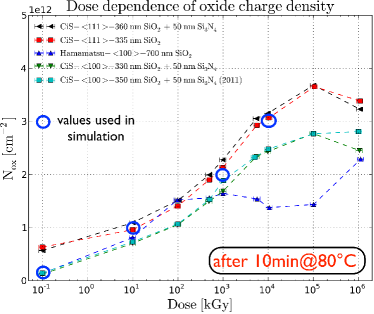
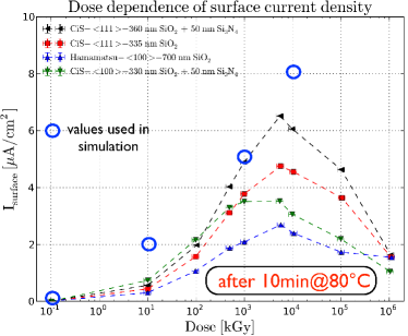
Measurements on test structures (MOS capacitors and gate-controlled diodes) have been used to determine the dose dependence of the density of oxide charges , and the surface-current density . The results are shown in figure 1 [7, 8]. In order to obtain reproducible results after irradiation, the test structures had to be annealed for 10 minutes at 80∘C [7]. It is found that increases with dose and saturates for doses above 10 MGy. The values for MOS capacitors from different vendors and for different crystal orientations show a spread of about a factor 2. In addition, annealing is observed already at room temperature [8]. also increases up to 10 MGy and then drops to lower values. The reason for this drop is not understood and still under study.
The values which were used in the TCAD simulations are indicated in the figure as circles. In the simulations it was assumed that is uniformly distributed along the Si-SiO2 interface. For the generation of the surface current the surface-recombination velocity with the elementary charge and the intrinsic charge-carrier density , was used. Details on the models for the device simulation and for the scaling of the 2D results to 3D for the pixels, can be found in [9]. The breakdown voltage was determined by the criterion
with the gradient of the current-voltage curve , and the ratio of the current to voltage .
3 Sensor optimization
Based on detector and science simulations [10], the AGIPD collaboration has specified the sensor parameters to be achieved for doses from 0 to 1 GGy listed in table 1.
| Parameter | Value |
|---|---|
| sensitive area | 10.52 2.56 cm2 |
| mechanical thickness | 500 20 m |
| distance pixel edges to cut edges | 1200 m |
| resistivity of doping | 3 - 8 kcm |
| pixel dimensions | 200 200 m2 |
| operating voltage | 500 V |
| breakdown voltage | > 900 V |
| coupling type | DC |
| inter-pixel capacitance@500V | < 500 fF |
| total sensor dark current@500V | < 50 A |
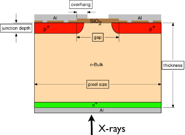
The parameters which have been optimized in the design of the sensor, some which are shown in figure 2, are for the pixels the gap, aluminum (Al) overhang and radius of junction and Al layer at the corners, for the guard-ring structure the number of rings, implantation widths, spacings and Al overhangs, and for the process parameters the depth of the junctions and the oxide thickness.
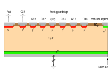
The performance parameters which have been optimized for doses between 0 and 1 GGy are the breakdown voltage, the leakage current and inter-pixel capacitance for the pixels, and the breakdown voltage and the voltage drop between the individual guard rings for the guard-ring structure.
Moreover, it has been ensured that the depletion boundary does not touch the scribe line.
The strategy applied for the optimization can be summarized as follows:
-
•
Guard ring (GR) optimization (2D simulations in (x,y) for the straight edges and in (r,z) for the corners):
-
1.
Optimize the breakdown voltage without guard ring (0 GR - only CCR) for different values of (, , , , and cm-2) as function of oxide thickness, junction depth and Al overhang.
-
2.
Estimate the number of floating GRs required for V.
-
3.
Vary the spacing between GRs, junction widths and Al overhangs, to achieve the maximum for a minimum width of the GR structure. This was achieved when the maximum electric fields in the gaps between the guard rings are approximately the same.
-
1.
-
•
Pixel optimization (2D simulations in (x,y)):
-
1.
Optimize the oxide thickness, Al overhang, gap and junction depth with respect to breakdown voltage, dark current and inter-pixel capacitance.
-
2.
Extrapolate the dark current and inter-pixel capacitances to 3D values.
-
3.
Check the breakdown voltage and dark current as function of voltage by a 3D simulation (only 1/4 pixel simulated).
-
1.
4 Results of the sensor optimization
4.1 Guard-ring structure
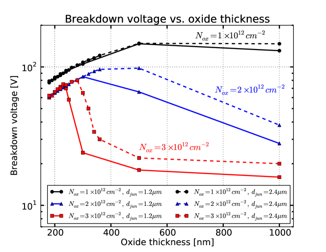
The breakdown voltage without guard ring (0 GR) as function of oxide thickness , for different oxide-charge densities , two junction depths and 2.4 m and an Al overhang of 5 m, is shown in figure 3. The breakdown voltages for values below cm-2 are above 180 V and are not shown. For cm-2 the values of increase from 80 V to 150 V when is increased. For higher values, reaches a maximum and then decreases. For cm-2 the value of drops from 70 V at nm, to 20 V at nm. This sudden decrease of is related to the electron-accumulation layer below the Al overhang: If an accumulation layer is present, there is a single high-field region at the edge of the junction. Without accumulation layer the voltage drop occurs over the entire region below the Al layer, with one high field region at the edge of the junction and a second one below the end of the Al overhang. In addition, a deeper junction results in a lower field at the edge of the junction, thus further increasing the breakdown voltage.
From the curves of cm-2 shown in figure 3, we conclude that the optimum value of the oxide thickness is 230 nm for a junction depth of 1.2 m, and 270 nm for 2.4 m. The corresponding breakdown voltages are between 70 and 80 V. This leads to the estimate that 15 floating GRs and a CCR are required to achieve a sensor-breakdown voltage of V.
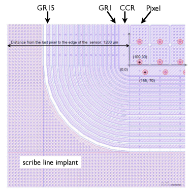
After choosing a junction depth of 2.4 m, an oxide thickness of 250 nm, and performing step 3 of the GR-optimization procedure, the following parameters for the optimized guard-ring structure have been determined:
-
•
Gap between pixels and CCR: 20 m.
-
•
Width of the junction of the CCR: 90 m.
-
•
Al overhang of CCR: 5 m.
-
•
Gap between CCR and 1st GR: 12 m.
-
•
Widths of the junctions of the GRs: 25 m.
-
•
Al overhangs towards pixel for GRs 1-15: 2, 3, 4,…, 16 m.
-
•
Al overhangs away from pixel for GRs 1-15: 5 m.
-
•
Gaps between GRs 1-2,2-3,…,14-15: 12, 13.5, 15, … 33 m.
A printout of the GDS file of the optimized guard-ring design is shown in figure 5 left. The simulated breakdown voltages of this structure for values of , and cm-2 and for different resistivities of the silicon are given in table 2. Shown are the results of 2D simulations in Cartesian coordinates (x,y) for the straight section of the guard rings, and in polar coordinates (r,z) for the corners. Given, that already 600 000 grid points are required for the 2D simulations, a 3D simulation of the guard-ring structure is not feasible. The results show that the minimum breakdown voltage is 830 V for a resistivity of 3 kcm and of cm-2. The breakdown voltage is above 900 V for resistivities of 5 and 8 kcm. Additional simulations with of cm-2 show that in the specified resistivity range of 3 to 8 kcm the depletion region does not touch the scribe line for voltages below 990 V. With increasing the extension of the depletion region towards the scribe line decreases.
| 3 kcm | 5 kcm | 8 kcm | ||||
|---|---|---|---|---|---|---|
| [cm-2] | 2D (x,y) | 2D (r,z) | 2D (x,y) | 2D (r,z) | 2D (x,y) | 2D (r,z) |
| V | 1060 V | V | V | V | V | |
| 1000 V | 830 V | 1080 V | 910 V | 950 V | 950 V | |
| 1010 V | 840 V | V | 910 V | 1000 V | 960 V | |
4.2 Pixel
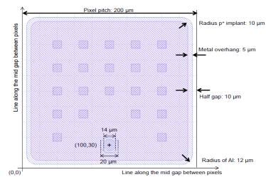
Because the pixel optimization is published in [9], here we only show that with above process parameters (junction depth of 2.4 m, oxide thickness 250 nm) and geometry parameters (gap of 20 m, Al overhang of 5 m, radius of junction of 10 m and radius of the Al layer of 12 m) the specification of table 1 are met. A printout of the GDS file of the optimized pixel layout is shown in figure 5 right.
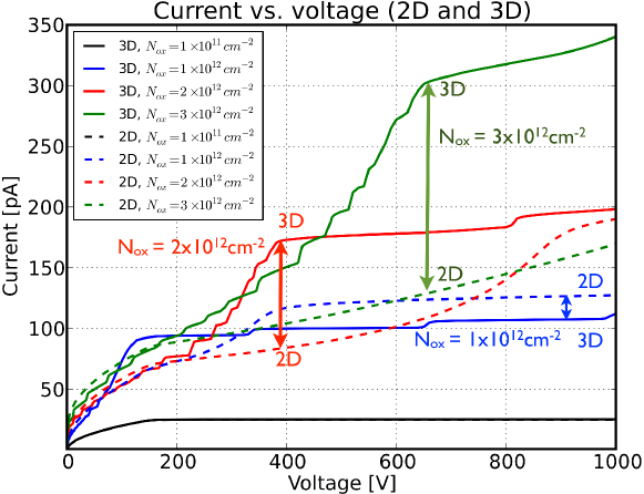
In figure 4 the I-V curves for 2D (x,y) simulations and for 3D simulations of a quarter of a pixel are plotted for the values of and given in table 3 for a resistivity of 5 kcm. The currents are scaled to the pixel size of 200 200 m2. The breakdown voltage of the pixels for this design is above 1000 V. The difference in the voltage dependence of the currents between the 2D and the 3D simulations for high values is due to the shape of the electron-accumulation layer at the corners of the pixel: The surface current is given by the product of the surface-current density times the area of the depleted surface at the Si-SiO2 interface. The corners of the pixels can only be properly simulated in 3D.
The inter-pixel capacitance , the sensor dark current and the CCR dark current are listed in table 3 for a voltage of 500 V and different values. All values are within the specifications.
| A/cm | A | A | [fF] | |
|---|---|---|---|---|
| 2 | 7.4 | 0.6 | 120 | |
| 5 | 12.7 | 0.9 | 270 | |
| 8 | 14.4 | 1.2 | 312 |
5 Summary
Experimental results on the dose dependence of the surface density of oxide charges and the surface-current density have been implemented in the SYNOPSYS TCAD simulation program and the design of the pixel and guard-ring layout for the AGIPD sensor has been optimized. The TCAD simulations show that the optimized sensor design meets the specifications for the AGIPD, in particular breakdown voltage, dark current and inter-pixel capacitance.
Acknowledgements.
This work was performed within the AGIPD Project financed by the European XFEL-Company. Additional support was provided by the Helmholtz Alliance Physics at the Terascale and J. Zhang was supported by the Marie Curie Initial Training Network MC-PAD. We thank the AGIPD colleagues for the excellent collaboration and the funding institutions for their support.References
- [1] M. Altarelli, et al., European X-ray free electron laser technical design report, Technical Report, The European XFEL, 2007.
- [2] B. Henrich et al., The adaptive gain integrating pixel detector AGIPD, a detector for the European XFEL, Nucl. Instr. Meth. A 633 (2011) S11-S14.
- [3] H. Graafsma, Requirements for and development of 2 dimensional X-ray detectors for the European X-ray Free Electron Laser in Hamburg, \jinst42009P12011.
- [4] Synopsys TCAD, webpage http://www.synopsys.com/.
- [5] A. Akkerman et al., Updated NIEL calculations for estimating the damage induced by particles and gamma-rays in Si and GaAs, Radiat. Phys. Chem. 62 (2001) 301.
- [6] T.R Oldham, Ionizing Radiation effects in MOS Oxides, World Scientific Publishing Co. (1999).
- [7] J. Zhang et al., Study of radiation damage induced by 12 keV X-rays in MOS structures built on high resistivity n-type silicon, J. Synchrotron Rad. 19 (2012) 340, arXiv:1107.5949.
- [8] J. Zhang et al., Investigation of X-ray Induced Radiation Damage at the Si-SiO2 Interface of Silicon Pixel Sensors for the European XFEL, 14th International Workshop on Radiation Imaging Detectors, 1-5 July 2012, Figueira da Foz, Coimbra, Portugal, paper submitted and arXiv:1210.0427.
- [9] J. Schwandt et al., Optimization of the Radiation Hardness of Silicon Pixel Sensors for High X-ray Doses using TCAD Simulations, \jinst72012C01006, arXiv:1111.4901.
- [10] G. Potdevin, U. Trunk, H. Graafsma, Performance simulation of a detector for 4th generation photon sources: The AGIPD, Nucl. Instr. Meth. A 607 (2009) 51-54.