Investigation of X-ray induced radiation damage at the Si-SiO2 interface of silicon sensors for the European XFEL
Abstract
Experiments at the European X-ray Free Electron Laser (XFEL) require silicon pixel sensors which can withstand X-ray doses up to 1 GGy. For the investigation of X-ray radiation damage up to these high doses, MOS capacitors and gate-controlled diodes built on high resistivity n-doped silicon with crystal orientations <100> and <111> produced by two vendors, CiS and Hamamatsu, have been irradiated with 12 keV X-rays at the DESY DORIS III synchrotron light source. Using capacitance/conductance-voltage, current-voltage and thermal dielectric relaxation current measurements, the surface densities of oxide charges and interface traps at the Si-SiO interface, and the surface-current densities have been determined as function of dose. Results indicate that the dose dependence of the surface density of oxide charges and the surface-current density depend on the crystal orientation and producer. In addition, the influence of the voltage applied to the gates of the MOS capacitor and the gate-controlled diode during X-ray irradiation on the surface density of oxide charges and the surface-current density has been investigated at doses of 100 kGy and 100 MGy. It is found that both strongly depend on the gate voltage if the electric field in the oxide points from the surface of the SiO to the Si-SiO interface. Finally, annealing studies have been performed at 60 ∘C and 80 ∘C on MOS capacitors and gate-controlled diodes irradiated to 5 MGy and the annealing kinetics of oxide charges and surface current determined.
keywords:
XFEL; radiation damage; oxide charge; interface trap; surface current; radiation-hard silicon sensor1 Introduction
At DESY, Hamburg, the European X-ray Free Electron Laser (XFEL) [1] is under construction. Starting in late 2015, it will open up completely new research opportunities for science as well as for industrial applications. Examples are the structural analysis of single complex organic molecules, the investigation of chemical reactions at the femtosecond scale, and the study of processes that occur in the interior of planets.
At the European XFEL, imaging experiments require silicon pixel detectors. One of the X-ray pixel detectors under development is the Adaptive Gain Integrating Pixel Detector (AGIPD) [2, 3], which has to satisfy extraordinary performance specifications [4]: Doses of up to 1 GGy in three years of operation, up to 105 12 keV photons per pixel of 200 m 200 m arriving within less than 100 fs, and a time interval between XFEL pulses of 220 ns. To address these challenges, radiation-hard silicon pixel sensors need to be developed, which requires good understanding of X-ray induced radiation damage.
The aim of this work is to (1) understand the radiation damage induced by X-rays, (2) extract the damage-related parameters, i.e. the surface density of oxide charges and surface-current density, which are the main inputs for sensor optimization with TCAD simulation [5], (3) investigate the effects due to the voltage applied to the gates of the MOS capacitor and the gate-controlled diode during irradiation, and (4) verify the long term stability and performance of silicon sensors with the help of annealing studies. The following sections will discuss the results for the above topics separately.
2 Radiation damage at the European XFEL environment
There are two kinds of radiation damage: bulk damage and surface damage. The former is due to the non-ionization energy loss (NIEL) [6, 7] of incident particles, i.e. protons, neutrons, electrons and gamma-rays, which cause silicon crystal damage; the latter is due to the ionization energy loss of charged particles or X-ray photons, which cause positive charges and traps to build up in the SiO2 and at the Si-SiO2 interface. The threshold energy for X-rays to cause bulk damage is 300 keV. Therefore, the main damage in silicon sensors at the European XFEL with a typical energy of 12 keV is the surface damage.
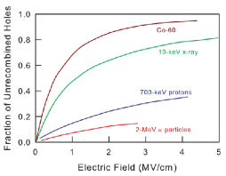
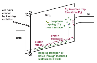
The mechanisms of surface damage have been described extensively in [8, 9, 10, 11, 12]. We shortly summarize them as follow: X-rays (or charged particles) produce electron-hole pairs in the SiO2. Depending on the strength of the electric field in the SiO2 and the type of incident particles, as seen in figure 1(a), a fraction of electrons and holes recombine. The remaining electrons and holes escaping from the initial recombination either drift to the electrode or to the Si-SiO2 interface, depending on the direction of the electric field in the SiO2. Some of the holes drift close to the interface, are captured by oxygen vacancies (most of the vacancies locate in the SiO2 close to the Si-SiO2 interface) and form trapped positive charges in the oxide, called oxide charges. During the transport of holes, some react with hydrogenated oxygen vacancies and result in protons. Those protons, which drift to the interface, break the hydrogenated silicon bonds at the interface and produce dangling silicon bonds, namely interface traps, with energy levels distributed throughout the band gap of silicon.
Figure 1(b) shows the mechanisms of formation of oxide charges (with density ) and interface traps (with density ) in a MOS capacitor biased with positive voltage. The values of and induced by X-ray ionizing radiation mainly depend on dose, electric field in the SiO2, annealing time and temperature, crystal orientation, and quality of the oxide. The influence of the above factors has been investigated and results will be discussed in Section .
3 Investigated structures and irradiation
To study the surface damage, test fields have been designed. Each test field includes a MOS capacitor and a gate-controlled diode. The MOS capacitor has a circular shape with a diameter of 1.5 mm. The gate-controlled diode contains a circular diode ( = 1.0 mm) in the center and 5 concentric surrounding gate rings. The width of the gate rings is 50 m and neighbouring gate rings are separated by 5 m spacing.
The investigated test fields fabricated on high resistivity n-type silicon with different orientations produced by two vendors, used for the study in Section , are listed in table 1. For the studies in Section and , the test fields with orientation <100> and <111> produced by CiS have been used, respectively.
| Label | CE2250 | CB0450 | 6336-01-03 | HAMA-MOS-04 |
| Producer | CiS [13] | CiS | CiS | Hamamatsu [14] |
| Material | FZ | DOFZ | Epi | FZ |
| Orientation | <100> | <111> | <111> | <100> |
| Doping | cm-3 | cm-3 | cm-3 | cm-3 |
| Insulator | 330 nm SiO2 | 360 nm SiO2 | 335 nm SiO2 | 700 nm SiO2 |
| + | + | |||
| 50 nm Si3N4 | 50 nm Si3N4 |
The irradiation of the test fields have been done at the DESY DORIS III beamline F4 with a "white" photon beam. The typical energy of the X-rays is 12 keV with a full width at half maximum of 10 keV. The flux at the beam center is approximately photons/(mms), which corresponds to a dose rate of 180 kGy/s in SiO2 . A chopper has been used to reduce the dose rate in order to avoid heating up the silicon during X-ray irradiation. The typical temperature during irradiations was in the range from 25 ∘C to 36 ∘C [15]. Details on the X-ray beam profile and dose calibration can be found in [15, 16].
The following procedures are used for the study in Section : (1) solid state measurements were performed on MOS capacitors and gate-controlled diodes before irradiation; (2) the test fields, each consisting of a MOS capacitor and a gate-controlled diode, were irradiated to a specific dose (the first irradiation dose is 10 kGy); (3) after irradiation, the solid state measurements were performed before and after annealing at 80 ∘C for 10 minutes111Annealing needs to be done in order to obtain reproducible results [17].; (4) the previously irradiated test fields were irradiated to higher doses and measured afterwards. The steps (2)-(4) were repeated till the 1 GGy dose had been reached. For the studies in Section and , only steps (1), (2) and (3) were done without repeat.
4 Methods to extract the parameters related to surface damage
4.1 Extraction of and
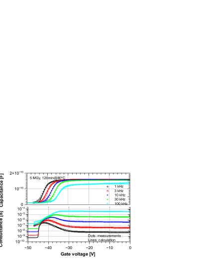
The capacitance/conductance-voltage (C/G-V) and thermal dielectric relaxation current (TDRC) measurements have been performed on the MOS capacitors, which are used to extract the surface density of oxide charges, , and the density of interface traps, . During the measurements, the voltage is applied to the gate of the MOS capacitor while the backside is grounded. The measurement procedures have been described in [16, 17]. The measured TDRC signal, , as function of temperature, , allows to determine the distribution of the density of interface states, , in the silicon band gap [18, 19, 20]. The total density of interface traps, , can be estimated by integrating the TDRC signal divided by the heating rate used in the measurement and the elementary charge : . To extract the surface density of oxide charges , a model describing the irradiated MOS capacitor by an RC-network is employed. The model allows to calculate the capacitance and conductance of a MOS capacitor as function of gate voltage for different frequencies using the measured TDRC signal and as input. , which just shifts the C/G-V curves along the voltage-axis, is obtained by adjusting its value till the calculated C/G-V curves describe the measurements. Figure 2(a) shows the comparison of the measured to the calculated C/G-V curves (parallel mode) of a MOS capacitor irradiated to 5 MGy after annealing for 120 minutes at 80 ∘C for frequencies between 1 kHz and 100 kHz. The model has been described in [17]. In the model calculations, all the interface traps within the silicon band gap are assumed to be acceptors, which gives the maximal estimate for the surface density of oxide charges introduced by X-rays.
4.2 Extraction of
To determine the surface-current density, , current-voltage (I-V) measurements have been done at room temperature for the gate-controlled diodes. For the I-V measurement, a constant DC voltage (-12 V in our case) is applied to the p+ electrode through a voltage source to partially deplete the central diode, and the current flow from the rear side n+ electrode is recorded as function of voltage on the 1st gate ring while keeping the 2nd gate ring grounded. The DC voltage applied to the p+ electrode should be enough so that the depletion regions below the diode and the 1st gate merge when the 1st gate is biased to depletion.
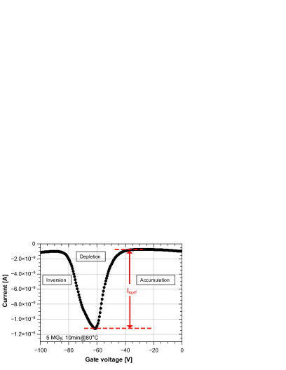
Figure 2(b) shows the I-V curve of a gate-controlled diode irradiated to 5 MGy after annealing for 10 minutes at 80 ∘C. The surface current, , is extracted from the "maximum" current measured in depletion of the 1st gate ring and the average value of the currents obtained in accumulation. It should be noted that the measured surface current is very sensitive to the temperature during the measurement, i.e. at room temperature its value changes by 8% if the temperature changes by 1 ∘C. In figure 3(a), the temperature dependence of the I-V curves of an irradiated gate-controlled diode measured at different temperatures from 213 K to 295 K is shown. The following scaling formula allows to describe the data
| (1) |
with the Boltzmann constant.
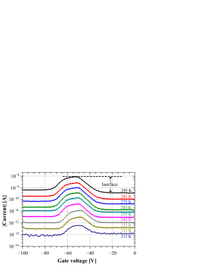
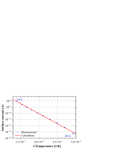
Figure 3(b) shows the comparison between the measured surface currents and the calculated ones according to the scaling formula 1 in the temperature range from 203 K to 295 K, which shows good agreement. Thus, all surface currents extracted from the measurements in our study have been scaled to the values at 20 ∘C. The surface-current density at 20 ∘C, , is calculated from the surface current scaled to 20 ∘C and the area of the 1st gate ring: .
5 Results
5.1 Dose dependence
We first present the results from MOS capacitors and gate-controlled diodes irradiated to eight X-ray doses in the range between 10 kGy to 1 GGy. During the irradiations, the electrodes of the MOS capacitors or the gate-controlled diodes were kept floating. The first C/G-V and I-V measurements were performed within 1 hour after each irradiation. As mentioned above, due to significant annealing of the radiation induced defects already at room temperature, measurements were also done after annealing at 80 ∘C for 10 minutes in order to obtain reproducible results. Hence, only the results after annealing will be shown in the following.
Figure 4 shows the surface density of oxide charges, , and the surface-current density, , as function of dose. A comparison of the measurements between cyan stars (CS: CiS-<100>-350 nm SiO2 + 50 nm Si3N4) and green dots (GD: CiS-<100>-330 nm SiO2 + 50 nm Si3N4) shows that the results for structures with the same technology and crystal orientation are compatible222The thickness of the SiO2 has been estimated from the capacitance of the MOS capacitor biased to accumulation assuming a Si3N4 thickness of 50 nm.. The results for CS, measured in 2011, are obtained from eight different MOS capacitors each one directly irradiated to the dose shown in figure 4(a). GD, measured in 2012, are the results from one MOS capacitor irradiated in steps to the doses given in the figure and annealed for 10 minutes at 80 ∘C after each step. Thus, it can be concluded that, under the same irradiation environment and annealing condition, the densities of defects introduced by X-ray ionizing radiation are independent of the way the irradiation is performed but depend on the "accumulated dose".
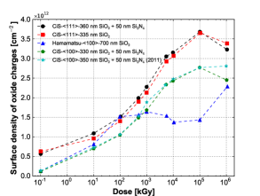
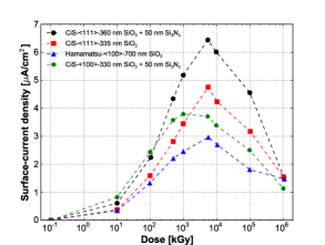
From the dose dependence of the surface density of oxide charges and the surface-current density , it is found that: (1) and for <100> silicon is lower than that for <111> silicon. (2) Little difference in is observed for the MOS capacitors with an insulating layer made of SiO2 and that made of SiO2 and Si3N4. (3) The values found for samples fabricated by CiS and Hamamatsu are different, agree however within a factor of 2, which indicates a dependence of radiation-induced defects on technology. (4) and either saturate or decrease at high irradiation doses. The significant decrease of at high doses is not understood and still under study.
5.2 Gate-voltage dependence
The presence of an electric field in the SiO2 during the irradiation plays an important role in the formation of oxide charges and interface traps: it determines not only the fraction of electrons and holes escaping from the initial recombination, but also the direction the electrons and holes drift, which impacts on the amount of oxide charges and interface traps that form in the Si-SiO2 interface region.
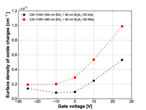
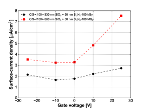
Figure 5 shows the gate-voltage dependence of the surface density of oxide charges, , and the surface-current density, , for doses of 100 kGy and 100 MGy. The maximum gate voltage used, 25 V, corresponds to an electric field of 0.7 MV/cm in the SiO2. The results will be discussed for three cases:
(i) For 0 V, the initial electric field in the SiO2 is zero and thus the situation is similar to the case without gate voltage applied. In both cases, the electric field in the SiO2 during irradiation is dominated by the field created by the oxide charges, which points from the Si-SiO2 interface to the aluminium gate. Hence, the values of and obtained under 0 V are similar to the values obtained without gate voltage (refer to the values of and at 100 kGy and 100 MGy in figure 4).
(ii) For negative gate voltages, the direction of the electric field in the SiO2 points from the Si-SiO2 interface to the aluminium gate, as for 0 V. The electric field in the SiO2 is the sum of the electric field due to external voltage and that created by the positive oxide charges close to the Si-SiO2 interface. With increasing "accumulated dose", the electric field due to the oxide charges increases; thus, the field due to the gate voltage is reduced. For example, the electric field created by the oxide charges with a density of cm-2 is 0.9 MV/cm if it is assumed that the oxide charges are located at the interface, compared to a field of 0.7 MV/cm for a gate voltage of -25 V. Therefore, no big difference is observed for the values of and obtained under negative gate voltage and under 0 V. However, the situation may change for a different spatial distribution of oxygen vacancies in the SiO2.
(iii) For positive gate voltages, the direction of the electric field in the SiO2 points from the aluminium gate to the Si-SiO2 interface. The number of holes drifting to the interface is larger than for negative or zero gate voltage. Thus, more holes are able to be captured by the oxygen vacancies located close to the interface and produce oxide charges. As the fraction of holes escaping from the initial recombination process increases with the electric field in the SiO2, the number of holes drifting to the interface increases with the positive gate voltage applied to the aluminium gate. Thus, a strong voltage dependence of and is observed in this case.
5.3 Time and temperature dependence of annealing
In order to understand the long term behaviour of the oxide charges and interface traps, annealing studies have been performed on MOS capacitors and gate-controlled diodes irradiated to 5 MGy. Different processes are responsible for the annealing of the oxide charges and interface traps.
The annealing of oxide charges is due to two different hole-removal processes [9]. Below 125 ∘C, the removal of oxide charges is mainly due to the recombination of trapped holes with electrons tunnelling into the SiO2 from the silicon, which has been described by a tunnelling model [21, 22]:
| (2) |
with . is the surface density of oxide charges at , the effective tunnelling time constant, the characteristic depth of the spatial distribution of oxide charges in the SiO2 and a parameter related to the barrier height, the tunnelling time constant, and the difference between the energy level of the defects in the SiO2 and the Fermi level in the silicon. Above 150 ∘C, a rapid removal or recombination of trapped holes in the SiO2 is observed, which is described by a thermal detrapping model [23].
The annealing mechanism of interface traps (dangling silicon bonds) is not well understood, but the kinetics can be described by the "two reaction model" according to [24, 25]. The first reaction is the passivation of dangling silicon bonds by hydrogen at the Si-SiO2 interface. The second reaction is the binding of two hydrogen atoms to a hydrogen molecule. The "two reaction model" predicts that the time dependence of the density of interface traps follows a power law. As the surface current is mainly generated by the interface states at the mid-gap of silicon, the annealing behaviour of the surface-current density is also described by a similar expression as for the annealing of :
| (3) |
with . is the surface-current density at , a parameter related to the ratio of the two reaction rates, the frequency factor and the activation energy.
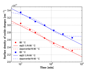
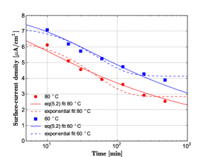
The annealing of oxide charges and interface traps in this study has been performed at 60 ∘C and 80 ∘C. Figure 6 shows and as function of annealing time. We fit to the measurements by the functions given in eq(2) and (3) and an exponential function, expected for a constant annealing probability. It can be seen that eq(2) and (3) provide a good description of the data supporting the tunnelling model and the "two reaction model". Table 2 and 3 show the parameters found from the fits for and by the functions given in eq(2) and (3). The data can be used to calculate the annealing behaviour of the oxide charges and the surface current at other temperatures. It is found that the annealing of is a slow process whereas the annealing of is relative fast. For example, using the parameters found it is predicted that it takes three years to remove 50% of the oxide charges at 20 ∘C but only 5 days to reduce the surface-current density by 50%.
| [cm-2] | [s] | [eV] | |
|---|---|---|---|
| [Acm-2] | [s] | [eV] | |
|---|---|---|---|
6 Summary and outlook
Results on the surface densities of oxide charges and the surface-current densities from MOS capacitors and gate-controlled diodes built on high resistivity n-type silicon with orientations <100> and <111> produced by two vendors, CiS and Hamamatsu, as function of 12 keV X-ray doses up to 1 GGy have been presented. The influence of the electric field in the oxide on the formation of oxide charges and interface traps has been investigated. Finally, first results on the annealing of the X-ray induced oxide charges and the surface current due to interface traps are presented.
Additional annealing studies will be performed for MOS capacitors and gate-controlled diodes irradiated to a dose of 100 MGy. The extracted parameters, extrapolated annealing behaviour at room temperature and detailed discussions will be reported in a separated paper.
Acknowledgements.
The work was performed within the AGIPD Project. J. Zhang would like to thank the Marie Curie Initial Training Network "MC-PAD" for his PhD funding. I. Pintilie gratefully acknowledges the financial support from the Romanian National Authority for Scientific Research through the Project PCE 72/5.10.2011. We would like to thank the colleagues within AGIPD collaboration for their helpful discussions on the results. The work was also supported by the Helmholtz Alliance "Physics at the Terascale".References
- [1] The webpage of the European XFEL GmbH: http://www.xfel.eu.
- [2] B. Henrich et al., The adaptive gain integrating pixel detector AGIPD - a detector for the European XFEL, Nucl. Instr. and Meth. A 633 (2011) S11-S14.
- [3] D. Greiffenberg, The AGIPD detector for the European XFEL, JINST 7 (2012) C01103.
- [4] H. Graafsma, Requirements for the development of 2 dimensional X-ray detectors for the European X-ray Free Electron Laser in Hamburg, JINST 4 (2009) P12011.
- [5] J. Schwandt et al., Optimization of the radiation hardness of silicon pixel sensors for high x-ray doses using TCAD simulations, JINST 7 (2012) C01006, arXiv: 1111.4901.
- [6] M. Moll, Radiation Damage in Silicon Particle Detectors - Microscopic Defects and Macroscopic Properties, PhD thesis, DESY-THESIS-1999-040 (1999) ISSN 1435-8085.
- [7] I. Pintilie et al., Radiation-induced point- and cluster-related defects with strong impact on damage properties of silicon detectors, Nucl. Instr. and Meth. A 611 (2009) 52-68.
- [8] E.H. Nicollian and J.R. Brews, MOS (Metal Oxide Semiconductor) Physics and Technology, New York: John Wiley and Sons (1982) ISSN 0-471-08500-6.
- [9] T.P. Ma and P.V. Dressendorfer, Ionizing Radiation Effects in MOS Devices and Circuits, New York: John Wiley and Sons (1989) ISBN 0-471-84893-X.
- [10] T.R. Oldham et al., An Overview of Radiation-Induced Interface Traps in MOS Structures, Internal Note of Harry Diamond Laboratories HDL-TR-2163 (1989).
- [11] T.R. Oldham and F.B. McLean, Total Ionizing Dose Effects in MOS Oxides and Devices, IEEE Trans. Nucl. Sci. 50 (2003) 483-499.
- [12] J.R. Schwank, Radiation Effects in MOS Oxides, IEEE Trans. Nucl. Sci. 55 (2008) 1833-1853.
- [13] The webpage of CiS Forschungsinstitut fuer Mikrosensorik und Photovoltaik GmbH: http://www.cismst.org.
- [14] The webpage of Hamamatsu Photonics: http://www.hamamatsu.com.
- [15] H. Perrey, Jets at Low Q2 at HERA and Radiation Damage Studies for Silicon Sensors for the XFEL, PhD thesis, DESY-THESIS-2011-021 (2011).
- [16] J. Zhang et al., Study of X-ray Radiation Damage in Silicon Sensors, JINST 6 (2011) C11013, arXiv: 1111.1180.
- [17] J. Zhang et al., Study of radiation damage induced by 12 keV X-rays in MOS structures built on high-resistivity n-type silicon, J. Synchrotron Rad. 19 (2012) 340-346, arXiv: 1107.5949.
- [18] J.G. Simmons and G.W. Taylor, Dielectric Relaxation and Its Effects on the Thermal Electric Characteristics of Insulators, Phys. Rev. B 6 (1972) 4804-4814.
- [19] J.S. Uranwala et al., Nonsteady-state techniques for determining the energy distribution of interface traps in MNOS (memory) devices, Appl. Phys. Lett. 26 (1975) 697-699.
- [20] H.A. Mar and J.G. Simmons, A Review of the Techniques Used to Determine Trap Parameters in the MNOS Structure, IEEE Trans. Electron Devices 24 (1977) 540-546.
- [21] A.J. Lelis et al., The Nature of the Trapped Hole Annealing Process, IEEE Trans. Nucl. Sci. 36 (1989) 1808-1815.
- [22] M. Schmidt and H. Koester, Hole Trap Analysis in SiO2/Si Structures by Electron Tunneling, Phys. Stat. Sol. (b) 174 (1992) 53-66.
- [23] T.R. Oldham et al., Spatial Dependence of Trapped Holes Determined from Tunnelling Analysis and Measured Annealing, IEEE Trans. Nucl. Sci. 33 (1986) 1203-1209.
- [24] M.L. Reed and J.D. Plummer, Chemistry of Si-SiO2 Interface Trap Reactions, J. Appl. Phys. 63 (1988) 5776-5793.
- [25] M.L. Reed, Models of Si-SiO2 Interface Reactions, Semicond. Sci. Technol. 4 (1989) 980-985.