Graphene terahertz uncooled bolometers
Abstract
We propose the concept of a terahertz (THz) uncooled bolometer based on n-type and p-type graphene layers (GLs), constituting the absorbing regions, connected by an array of undoped graphene nanoribbons (GNRs). The GLs absorb the THz radiation with the GNR array playing the role of the barrier region (resulting in nGL-GNR-pGL bolometer). The absorption of the incident THz radiation in the GL n- and p- regions leads to variations of the effective temperature of electrons and holes and of their Fermi energy resulting in the variation of the current through the GNRs. Using the proposed device model, we calculate the dark current and the bolometer responsivity as functions of the GNR energy gap, applied voltage, and the THz frequency. We demonstrate that the proposed bolometer can surpass the hot-electron bolometers using traditional semiconductor heterostructures.
I Introduction
Owing to the gapless energy spectrum 1 , graphene layers (GLs) absorb electromagnetic radiation in a wide spectral range (from the ultraviolet to terahertz) due to the interband transitions 2 ; 3 ; 4 . Therefore, GLs can be used in photodetectors, light sources, modulators, and mixers using the interband transitions 5 ; 6 ; 7 ; 8 ; 9 ; 10 ; 11 ; 12 ; 13 ; 14 ; 15 ; 16 ; 17 . The performance of these devices can be enhanced by utilizing multiple-GL structures 18 . For the infrared and visible spectral ranges, the interband absorption prevails over the intraband (Drude) absorption. However, in the terahertz (THz) range, especially at low THz frequencies, the Drude absorption can dominate. The intraband absorption in GLs can also be used in different devices for THz modulation and detection. The THz detectors, including uncooled detectors, exploiting the effect of electron or hole heating (hot-electron or hot-hole bolometers) in two-dimensional electron (hole) heterostructures made of A3B5, CdHgTe, and other compound systems were realized previously 19 ; 20 ; 21 ; 22 ; 23 . In this paper, we propose and analyze THz uncooled bolometric detectors based on GL structures. We demonstrate that such bolometers can exhibit fairly high responsivity, effectively operating at room temperatures and surpassing THz bolometers based on the traditional semiconductor heterostructures. The main advantages of GL-based room temperature bolometers are associated with the following three factors: (i) high electron and hole THz conductivities at room temperature 1 and, hence, elevated Drude absorption; (ii) the dominant mechanism establishing the interband and intraband equilibrium is the interaction with optical phonons 24 ; 25 ; (iii) long time of the electron and hole energy relaxation via optical phonons due to their large energy meV 1 (this time is proportional to a factor and is very large for GLs even at room temperature K).
II Model and main equations
Figures 1(a) and 1(b) show the proposed nGL-GNR-pGL bolometers. The bolometers consist of two gapless n-type and p-type GL absorbing regions connected by an undoped array of GNRs with sufficiently large energy gap (serving as the barrier region). The GLs can be doped chemically [as in Fig. 1(a)] or ”electrically” (using the conducting gates with the bias voltages, , of different polarity, as shown in Fig. 1(b)). The gates which control the electron and hole densities can be made using GLs 17 ; 26 ; 27 . It is assumed that the GNR width, , is sufficiently small, so that the energy gap , (where cm/s is the characteristic velocity of electrons and holes in GLs) is large enough to provide essential confinement of electrons in the n-GL and holes in the p-GL due to the formation of the barrier. The room temperature operation of field-effect transistors with sub 10 nm GNRs exhibiting fairly large energy gap was reported in Ref. 28 . The energy barrier in such GNRs ensures a relatively strong dependence of the current on the effective temperature of electrons and holes enhancing the bolometer responsivity.
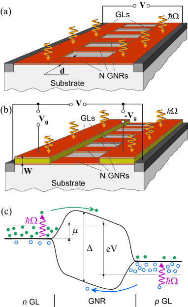
Figure 1(c) shows the resulting device band structure at sufficiently large bias voltage , where is the built-in voltage, is the Fermi energy of electrons and holes in GLs in equilibrium, and is the electron charge.
In the following, we assume that the interband absorption is relatively weak in comparison with the intraband absorption. This occurs when the energy of photons, , of the incident THz radiation is relatively small (corresponding to the frequency about few THz and lower). If , the interband transitions are forbidden due to the Pauli blocking. We assume that due to relatively high electron and hole densities, the intercarrier scattering time is sufficiently short to provide fast Maxwellization (or Fermization) of the photoexcited electrons and holes. Therefore, the electron and hole systems in GLs are characterized by quasi-Fermi energy and by the effective temperature . The heating of the electron and hole gases in the pertinent sections, i.e., the deviation of the effective temperature from the lattice temperature leads to the deviation of the Fermi energy from its equilibrium (dark) value . The quantities and are related by the following equation:
| (1) |
In the case of chemical doping, the quantity is equal to the donor (acceptor) density. In the detectors with electric doping, is given by , so that , where and are the dielectric constant and the thickness of the layer separating GLs and the gates and is the gate voltage [see Fig. 1(b)]. In the case under consideration, the electron and hole systems are sufficiently strongly degenerated (), hence, the Fermi energy is given by .
Considering the one-dimensional electron and hole transport in GNRs and the Fermi distributions of electrons and holes in GLs, in particular, near the GNR edges at , the sum of the electron and hole currents (i.e., the terminal current) between the p- and n-regions through parallel GNRs is equal to
| (2) |
Here is the kinetic energy of electrons and holes in GNR. In the absence of illumination, i.e., when and , Eq. (2) yields the following expression for the dark current :
| (3) |
Setting meV, and , for K we obtain A. This value is in a good agreement with experimental results 28 .
At relatively weak irradiation, and . Considering this, the variation of the current through the GNR array, , i.e., the photocurrent, can be presented in the following form:
| (4) |
The first and the second terms in the right-hand side of Eq. (4) describe the effect of variation of the effective temperature and the quasi-Fermi energy due to heating by the THz radiation. However, as follows from Eq. (1), when , the variation of the quasi-Fermi energy is relatively small, hence, the last term in the right-hand side of Eq. (4) can be omitted. Considering that the energy relaxation due to the processes governed by the interaction with optical phonons, the electron and hole effective temperature and the number of optical phonons obey the following equations:
| (5) |
| (6) |
Here, is the THz photon flux, , where , is the electron charge, is the speed of light, is the rate of the intraband transitions involving the emission and absorption of optical phonons, is the rate of optical phonon decay, and is proportional to the GL Drude ac conductivity 29 ; 30 :
| (7) |
where is the momentum relaxation time of electrons and holes, which, generally, is depending on and . Equations (5) and (6) govern the balance of the energy of the electron-hole system and the number optical phonons in GLs explicitly accounting for all the energy received by the electron-hole-optical phonon system from THz radiation going eventually to the thermostat.
Since , the expression for the term can be simplified 31 :
| (8) |
Here, is the time of the intraband phonon-assisted processes: the quantity plays the role of the effective energy relaxation time of electrons and holes. In equilibrium, Eqs. (5) and (6) yield and .
For the rate of optical phonons decay due to the unharmonic contributions to the interatomic potential, resulting in the phonon-phonon scattering, one can use the following simplified equation:
| (9) |
where is the decay time of optical phonons and is the number of optical phonons in equilibrium. Considering high heat conductivity of GLs 32 , the lattice temperature, i.e. the temperature of acoustic phonons, is assumed to be equal to the temperature of the contacts .
III Photocurrent and responsivity
Using Eqs. (4)-(9), we obtain
| (10) |
Here we also have introduced the rate of the generation of the electron-hole pairs due to the absorption of equilibrium optical phonons and parameter , where is the time of the interband transitions. The difference between and is due to the features of the density of states in GLs. At , one obtains 33 . The quantity weakly decreases with increasing the majority carrier concentration (if ) and strongly (exponentially) drops with decreasing temperature. At room temperature cm-2s-1 (compare with 24 ).
One can see from Eq. (10) that the intraband absorption of THz radiation leads to an obvious increase of the effective temperature .

Substituting from Eq. (10) into Eq. (4), we obtain
| (11) |
Here
| (12) |
Using Eqs. (11) and (12), for the bolometer current responsivity ( is the area of GLs), we obtain
| (13) |
For instance, considering a quasi-optic THz bolometer with a single GNR () integrated with a spiral antenna, we can assume that s, , m2, (about that in 22 ; 23 , K, and THz. Setting meV, meV, and cm-2s-1, we find A/W. If the applied bias voltage mV, setting A, for the voltage responsivity we obtain V/W. The later values of the current and voltage responsivities significantly exceed those for uncooled hot-electron bolometers based on the heterostructures made of the standard semiconductor (for example, CdHgTe hot-electron bolometers 22 ).
Using Eqs. (3) and (13), one can calculate the bolometer dark current limited detectivity . Since and , (for fixed ). At fixed value of , the detectivity achieves its maximum at .
Equation (12) shows that the heating of the optical phonon system due to the energy which this system receives from heated electrons and holes promotes an increase in the responsivity. The relative contribution of the optical phonon heating is determined by the factor . This implies that the bolometric effect in question is not purely a hot-electron or hot-hole effect. The bolometer spectral characteristic is determined by the frequency dependence of the ac Drude conductivity, which, as seen from Eq. (13) at , results in . If s, the responsivity roll-off occurs at THz.
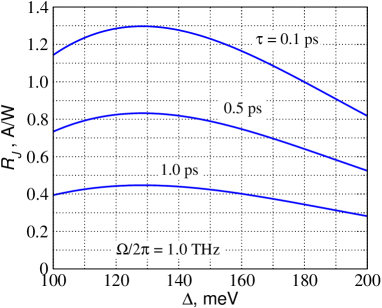
Figures 2 and 3 show the dependences of the responsivity and detectivity, respectively, on the energy gap in GNR, , calculated for the THz bolometers with and different momentum relaxation times for THz. It is assumed that meV and cm-2s-1.
According to Eq. (13), the responsivity increases with increasing number, , of GNRs, if the GL area is fixed. However, an increase in may require the related increase in the width of GLs and, consequently, in their area.
Similar bolometer can be based on n-GNR-n heterostructures. The results obtained above can also be applied to this device with small modifications: the dark current and responsivity given by Eqs. (3) and (13) should be multiplied by a factor , because the terminal dark current and photocurrent are due to the electrons injected from only one GL.
IV Conclusion
In conclusion, novel THz uncooled bolometers based on nG-GNR-pG heterostructures have been proposed. Using the developed model, we calculated the bolometer dark current and responsivity and demonstrated that nGL-GNR-pGL can surpass the hot-electron bolometers based on traditional semiconductor heterostructures.
V Acknowledgment
This work was supported by the Japan Society for Promotion of Science and TERANO-NSF grant, USA. The work at RPI was supported by NSF and ARL Alliance Cooperative Research Agreement program.
References
- (1) A. H. Castro Neto, F. Guinea, N. M. R. Peres, K. S. Novoselov, and A. K. Geim, Rev. Mod. Phys. 81, 109 (2009).
- (2) F. Bonnaccorso, Z. Sun, T. Hasan, and A. C. Ferrari, Nature Photonics, 4, 611 (2010).
- (3) R. R. Nair, P. Blake, A. N. Grigorenko, K. S. Novoselov, T. J. Booth, T. Stauber, N. M. R. Peres, and A. K. Geim, Science 320, 1308 (2008).
- (4) J. M. Dawlaty, S. Shivaraman, J. Strait, P. George, M. Chandrashekhar, F. Rana, M. G. Spencer, D. Veksler, and Y. Chen, Appl. Phys. Lett. 93, 131905 (2008).
- (5) F. T. Vasko and V. Ryzhii, Phys. Rev. B 77, 195433 (2008).
- (6) A. Satou, F. T. Vasko, and V. Ryzhii, Phys. Rev. B 78, 115431 (2008).
- (7) V. Ryzhii, V. Mitin, M. Ryzhii, N. Ryabova, and T. Otsuji, Appl. Phys. Express 1, 063002 (2008).
- (8) F. Rana, IEEE Trans. Nanotechnol. 7, 91 (2008).
- (9) V. Ryzhii and M. Ryzhii, Phys. Rev. B 79, 245311 (2009).
- (10) F. Xia, T. Murller, Y.-M. Lin, R. Golizadeh-Mojarad, M. Freitag, Y.-M. Lin, J. Tsang, V. Perebeinos, Ph. Avouris, Nano Lett. 9, 1039 (2009).
- (11) J. Park, Y. H. Ahn, and C. Ruiz-Vargas, Nano Lett. 9, 1742 (2009).
- (12) F. Xia, T. Murller, Y.-M. Lin, A. Valdes-Garsia, and F. Avouris, Nat. Nanotechnol. 4, 839 (2009).
- (13) V. Ryzhii, M. Ryzhii, V. Mitin, and T. Otsuji, J. Appl. Phys. 106, 084512 (2009).
- (14) T. Mueller, F. Xia, and P. Avouris, Nat. Photon. 4, 297 (2010).
- (15) V. Ryzhii, M. Ryzhii, N. Ryabova, V. Mitin, and T. Otsuji, J. Infrared Phys. and Technol. 54, 302 (2011).
- (16) V. Ryzhii, N. Ryabova, M. Ryzhii, N. V. Baryshnikov, V. E. Karasik, V. Mitin, and T. Otsuji, Optoelectronics Review 20, 15 (2012).
- (17) M. Liu, X. Yin, and X. Zhang, Nano Lett. 12, 1482 (2012).
- (18) M. Orlita and M. Potemski, Semicond. Sci. Technol. 25, 063001 (2010).
- (19) X. G. Peralta, S. J. Allen, M. C. Wanke, N. E. Harff, J. A. Simmons, M. P. Lilly, J. L. Reno, P. J. Burke, and J. P. Eisenstein, Appl. Phys. Lett. 81, 1627 (2002).
- (20) E. A. Shaner, M. Lee, M. C. Wanke, A. D. Grine, J. L. Reno, and S. J. Allen, Appl. Phys. Lett. 87, 193507 (2005).
- (21) V. Ryzhii, A. Satou, T. Otsuji, and M. S. Shur, J. Appl. Phys. 103, 014504 (2008).
- (22) A. Dobrovolsky, F. Sizov, V. Zabudsky, and N. Momot, Terahertz Sci. Technol. 3, 33 (2010).
- (23) A. Hammar, S. Bevilacqua, V. Drakinsky, J. State, and A. Kalabuhov, IEEE Trans. Terahertz Sci. Technol. 1, 395 (2011).
- (24) F. Rana, P. A. George, J. H. Strait, S. Shivaraman, M. Chanrashekhar, M. G. Spencer, Phys. Rev. B 79, 115447 (2009).
- (25) R. S. Shishir, D. K. Ferry, and S. M. Goodnick, J.Phys.: Conf. Ser. 193, 012118 (2009).
- (26) N. Kharche and S. K. Nayak, Nano Lett. 11, 5274 (2011).
- (27) V. Ryzhii, T. Otsuji, M. Ryzhii, and M. S. Shur, J. Phys. D 45, 3201 (2012).
- (28) X. Wang, Y. Ouyang, X. Li, H. Wang, J. Guo, and H. Dai, Phy. Rev. Lett. 100, 206803 (2008).
- (29) L. A. Falkovsky and A. A. Varlamov, Eur. Phys. J. B 56, 281 (2007).
- (30) V. Ryzhii, M. Ryzhii, A. Satou, T. Otsuji, A. A. Dubinov, and V. Ya. Aleshkin, J. Appl. Phys. 106, 084507 (2009).
- (31) V. Ryzhii, M. Ryzhii, V. Mitin, and T. Otsuji, J. Appl. Phys. 110, 094503 (2011).
- (32) A.A. Balandin, S. Ghosh, D.L. Nika and E.P. Pokatilov, Fullerenes, Nanotubes and Carbon Nanostructures, 18, 474 (2010).
- (33) V. Ryzhii, M. Ryzhii, V. Mitin, A. Satou, and T. Otsuji, Jpn. J. Appl. Phys. 50, 094001 (2011).