Oxidation effects on graded porous silicon anti-reflection coatings
Abstract
Efficient anti-reflection coatings (ARC) improve the light collection and thereby increase the current output of solar cells. By simple electrochemical etching of the Si wafer, porous silicon (PS) layers with excellent broadband anti-reflection properties can be fabricated. In this work, ageing of graded PS has been studied using Spectroscopic Ellipsometry, Transmission Electron Microscopy and X-ray Photoelectron Spectroscopy. During oxidation of PS elements such as pure Si (Si0), Si2O (Si+), SiO (Si2+), Si2O3 (Si3+), and SiO2 (Si4+) are present. In addition both hydrogen and carbon is introduced to the PS in the form of Si3SiH and CO. The oxide grows almost linearly with time when exposed to oxygen, from an average thickness of 0 - 3.8 nm for the surface PS. The oxidation is then correlated to the optical stability of multi-layered PS ARCs. It is found that even after extensive oxidation, the changes in the optical properties of the PS structures are small.
I Introduction
Good anti-reflection coatings (ARC) can improve the light collection and thereby increase the efficiency of solar cells considerably. Porous Silicon (PS) multilayers have excellent broadband anti-reflective properties, and can be made using electrochemical etching of Si wafers in an electrolyte containing hydrofluoric acid (HF). However, the structure is very sensitive to etching parameters such as current density, electrolyte composition, temperature and substrate doping Zhang (2004); Rossow et al. (1995a).
Several groups have reported results from using PS as antireflection coating in solar cells Yuan et al. (2009); Kwon et al. (2007); Lipinski et al. (2003); Yerokhov et al. (2000); Bilyalov et al. (2000); Selj et al. (2010). We have previously shown that graded PS ARCs with an effective reflection of 3 % over the solar spectrum can be produced in p+ material. PS has a very high internal surface area, 200-600 m2/cm3, and is therefore significantly more reactive than bulk SiHerino et al. (1987). In order for these structures to be used in a solar cell device, the electrical and optical properties must not degrade with ageing. Extensive oxidation has been shown by Canham et al. Canham (1997) to occur even in air ambient at room temperature, but strong dependence of the oxidation process on the porosity, morphology, thickness, and storage of the PS structures are observed.
Oxidation of PS can take place both through continued SiO2 formation and formation of Ox-Si-H groups. Grosman and Ortega Grosman and Ortega (2006a) reported that the natural oxidation of PS forms SiO2 together with Si-OH and SiO2-OH, where Si is bounded to one or three oxygen atoms Grosman and Ortega (2006a), in addition to SiHx (x= 1, 2, 3) groups Grosman and Ortega (2006b); Rao et al. (1990). Domashevskaya at al. Domashevskaya et al. (1998) found the presence of (CH3CH2)3SiOH compounds in addition to amorphous Si (Si:H) in PS layers using XPS. More common compounds found in oxidized Si samples are Si2O, SiO, Si2O3, and SiO2 Peden et al. (1993); Himpsel et al. (1988); Thøgersen et al. (2008). In this paper, Spectroscopic Ellipsometry (SE), Transmission Electron Microscopy (TEM) and X-ray Photoelectron Spectroscopy (XPS) have been used to study the various oxidation states present before and after ageing of PS, and the effect upon the optical properties.
II Experimental
The electrochemical etching was performed using a double cell anodic etching system PSB Plus 4 from advanced micromachining tools (AMMT). Prior to etching, the wafers were dipped in 5% HF to remove native oxide and to clean the samples. The electrolyte consisted of 49 wt % HF and ethanol (C2H5OH) in a volume ratio 2:3, giving a HF concentration of about 20%. The wafers used were boron doped, 300-350 m thick, one side polished, monocrystalline Si with a (100) orientation. PS is formed on the polished side of the wafer without any additional texturing. The resistivity of the wafers was determined by four point probe to be 0.012-0.018 cm, which corresponds to a doping level of approximately 5x10¹⁸. In order to simplify the identification and quantification of oxidation effects from the SE measurements, homogeneous PS layers were used. Five homogeneous PS samples were etched under galvanostatic conditions, at a current density of 50 mA/cm2 for 15 s. The single layer samples have approximately the same average porosity as the graded PS ARCs. Etching of the graded PS ARC structures is also performed in galvanostatic mode, by stepwise variation of the current density. Details of the procedure, such as the duration and current density of each step are described elsewhere Selj et al. (2010). Only the current density during etching is different for the homogeneous and multilayered samples and the average porosities of the two are similar.
The first homogeneous sample (Day 0) was rinsed in water, dried in N2 and stored in aluminium foil during transportation to the XPS. This was done in order to achieve a minimally oxidized starting sample. All remaining samples were rinsed in ethanol and air dried. Ethanol has a reduced surface tension compared to water and therefore reduces the risk of surface cracking and flaking of the PS films. The samples were stored in in air at room temperature.
Depth profile XPS was carried out by sputtering the surface using an Ar beam. Since this process alters the surface of the sample, one single sample could not be used for all measurements. Five nominally identical samples were therefore used for XPS. We have previously shown that the PS layers used in this work are reproducible to within an uncertainty of 1.5 % (90 % cl.) in thickness and porosity Selj et al. (2011).
The different elements present after the oxidation of PS have been studied by XPS. XPS was performed in a KRATOS AXIS ULTRADLD using monochromated Al K radiation (h =1486.6 eV) on plane-view samples at zero angle of emission (vertical emission). The x-ray source was operated at 1 mA and 15 kV. Depth profile sputtering was performed using a 4 kV ion gun, with a current of 100 A and a 500s cycle time. The etch depth was estimated to be approximately 100 nm. The mean free path () of Si-2p electrons in Si is 3.18 nm. This means that the photoelectron escape depth in Si is 3) = 9.54 nm, with . The spectra were peak fitted using CasaXPS http://www.casaxps.com after subtraction of a Shirley type background. Cross-sectional TEM samples were prepared by ion-milling using a Gatan precision ion polishing system with 5 kV gun voltage. The samples were analysed by HRTEM in a 200 keV JEOL 2010F microscope with a Gatan imaging filter and detector.
Ellipsometry measurements were carried out using a Woollam variable angle spectroscopic ellipsometer (WVASE) in the wavelength range 3001200 nm and at the angles of incidence 60∘, 65∘, 70∘, 75∘, and 80∘. Depolarization data is also collected for all samples. A model consisting of Si and voids in a Bruggeman effective medium approximation (EMA) provided a good fit to all the ellipsometric data sets Pettersson et al. (1998); Rossow et al. (1995b). Finally, reflectance was measured using a Standford Research System set-up in the wavelength range 4001100 nm.
III Results and Discussion
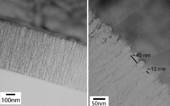
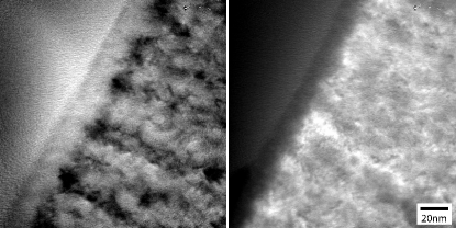
Two representative TEM images of the PS samples are shown in Figure 1. The PS layers are about 500 nm thick, with a pore size between 10-40 nm in diameter. A detailed study of the oxidation states and compounds present during ageing has been carried out using XPS. The SiOx thickness has also been calculated, and correlated to changes in porosity and refractive index during ageing. Energy Filtered TEM images in Figure 2 shows the SiOx thickness of the sample aged 42 days. Figure 2a filters the plasmon peak of SiO2 at 23 eV, while Figure 2b the plasmon peak of Si at 16 eV. The images clearly shows that the 15 nm thick layer outside the PS is due to SiOx and not to amorphous.
III.1 Peak-fitting Porous Silicon spectra
The Si-2p XPS spectra of both bulk and surface PS are shown in Figure 3, for samples exposed to oxygen for 0, 1, 7, 21 and 42 days. The XPS measurements of surface PS will collect photoelectrons down to a depth of about 20 nm, while the XPS spectra of bulk PS have been obtained after sputtering down to a depth of about 100 20 nm. In order to find all possible compounds present in the PS samples, a detailed peak fitting was carried out.
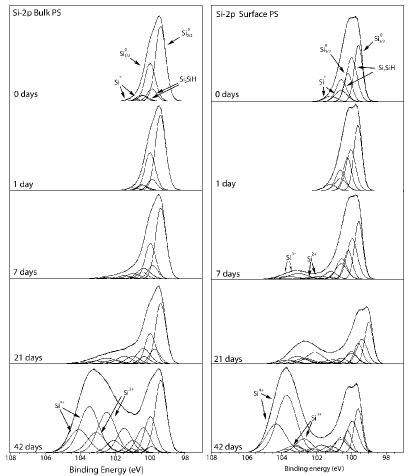
Cerofolini et al. Cerofolini et al. (2003) and Lu et al. Lu et al. (1993) showed a detailed peak fitting of the Si-2p spectra. A pure Gaussian function was shown to have the best fit for all oxide peaks. However, for bulk Si, an asymmetrical peak with a tail length of 6.5, tail scale of 0.6% and 70% Gaussian has been found to provide the best fit (GL(30)T(6.5)). The Si-2p1/2 and Si-2p3/2 were first fitted using this data, with a relative intensity of 1:2 (Si-2p1/2 / Si-2p3/2) Pleul et al. (2003). The SiOx peaks (Si+, Si2+, Si3+ and Si4+) were then fitted with a pure Gaussian function GL(0). The full width half maximum (FWHM) was set at 0.65 eV as has been reported for the Si-2p1/2 and Si-2p3/2 by Peden et al.Peden et al. (1993) and Himpsel et al. Himpsel et al. (1988). The binding energy of the 2p1/2 and 2p3/2 has been reported to be between 99.0 100.5 eV Cerofolini et al. (2003), while the binding energy of Si-2p for SiO2 is 103.6 eV Wagner et al. (1982). The chemical shift (EB(Si4+) - EB(Si0)) between the Si-2p1/2 and Si-2p3/2 is reported to be 0.6 eV with a FWHM of 0.65 eV Peden et al. (1993); Himpsel et al. (1988). The FWHM of the other oxidation states of Si were then found by comparing their relative sizes to our previous study for non-monochromatic XPS on Si Thøgersen et al. (2008). The appropriated FWHM values for the Si2O, SiO, Si2O3, and SiO2 were found to be 0.8 eV, 1.1 eV, 1.1 eV, and 1.2 - 1.5 eV respectively. There is a small difference in FWHM for surface PS and bulk PS, 0.55 eV and 0.70 eV respectively. The XPS spectra of surface and bulk PS were fitted to Si-2p3/2 peaks with a binding energy of 99.4, 100.4 eV, 101.4 eV, 102.5 eV, 103.6 eV, and 99.7 eV. The five first peaks correspond to pure Si (Si0), Si2O (Si+), SiO (Si2+), Si2O3 (Si3+), and SiO2 (Si4+). That leaves the peak with a binding energy of 99.7 eV.
III.1.1 Discussion of peak positions and FWHM
The fitted peak positions and FWHM is presented in Table 1 for all oxidation states. Oxidation states such as Si3SiH, Si2SiH2 or Si3SiC may also occur due to HF etching and C contamination at the surface Cerofolini et al. (2003). Si3SiH can be due to elemental silicon bonded to one hydrogen atom, and has 0.3 eV higher binding energy than for elemental silicon, while the compound Si2SiH2 has a 0.57 eV higher binding energy Cerofolini et al. (2003). The peak located at 99.7 eV has a 0.3 eV higher binding energy than elemental Si, which means that it is probably due to Si3SiH.
| Ox. state | EB | EB | FWHM |
| [eV] | [eV] | [eV] | |
| Si2p: Si0 | 99.4 | 100.0 | 0.55-0.7 |
| Si2p: Si+ | 100.4 | 101.0 | 0.8 |
| Si2p: Si2+ | 101.4 | 102.0 | 1.1 |
| Si2p: Si3+ | 102.5 | 103.1 | 1.1 |
| Si2p: Si4+ | 103.6 | 104.2 | 1.2-1.5 |
| Si2p: Si3SiH | 99.7 | 100.3 | 0.7 |
| O1s:SiOx | 532.5 | 1.5 | |
| O1s: C-OH | 533.4 | 1.4 | |
| C-O-C | |||
| O1s:C=O | 531.8 | 1.4 | |
| C1s: C | 284.5 | 1.2 | |
| C1s: C-O-C | 286.5 | 1.3 |
XPS spectra of the O1s peak for surface and bulk PS is presented in Figure 4 together with the surface PS spectra of the C1s peak. The O1s spectrum of both surface and bulk PS have two clear peaks. The O1s peak from SiO2 has a reported binding energy of 533.05 eV Hollinger et al. (1975). The O1s binding energy from C=O is reported to be between 531.2 531.6 eV, from C-OH and/or C-O-C between 532.2 533.4 eV, and for chemisorbed oxygen and perhaps some adsorbed water between 534.6535.4 eV Yue et al. (1999). The large peak at a binding energy of 532.5 eV seems to fit well with SiOx. The smaller peak at higher binding energy may therefore be due to C-OH and/or C-O-C. Bulk PS after 42 days shows an additional peak at 531.7 eV, which may be due to C=O. Figure 4 also shows the C1s peak of surface PS. The spectra can be fitted with two peaks located at a binding energy of 284.5 eV and 286.5 eV. Graphitic carbon has been reported to have a C1s binding energy of 284.6 eV, while CO between 290.4 290.8 eV Yue et al. (1999). From the O1s peaks the composition C-OH and/or C-O-C was identified. This composition can have a slightly smaller binding energy than CO, which would fit better with the observed binding energy. The two peaks may therefore correspond to pure C and C-OH and/or C-O-C.

There was a 0.15 eV difference in FWHM of Si0 between surface and bulk. Guerrero-Lemus et al Guerrero-Lemus et al. (1999) have studied the composition of PS using XPS and FTIR. They reported that XPS peaks in the Si-2p spectra can be attributed to Si-H bonds, in addition to amorphization of Si, due to a broadening of the Si peak. The presented Si-H peak is not shown clearly in the XPS spectrum, especially since there has been no peak fitting. In addition, no binding energy or FWHM values of the fitted peaks have been presented and compared to reference values. Ley et al. Ley et al. (1982) studied amorphous Si and found that the broadening in the XPS Si-2p peaks was due to a distribution of chemically shifted Si-2p lines. This shift occurred because of random charge fluctuations as the result of bond length variations in the amorphous network. However, a decrease of broadening was found in proportion to the number of hydrogen atoms attached to the silicon atom (Si, Si-H, Si-H2, Si-H3) due to charge transfer from Si to H. A small difference in FWHM between pure Si and Si-H was found to be 0.128 eV, a difference between a-Si and Si was 0.256 eV, while between a-Si:H and pure Si a difference of 0.186 eV was found. If the broadening in the Si2p peak for bulk PS for our data is due to Si-H bonds, the FHWM would decrease with time as the sample oxidises.
However, the fitted FWHM value is stable for all samples. Depth profile Ar sputtering of PS may however lead to a creation of amorphous Si (aSi) or amorphous hydrogenated Si (aSi:H). Ley et al. Ley et al. (1982) reported that these compounds have a 0.186 eV and 0.256 eV difference in binding energy compared to bulk crystalline Si. This broadening of the Si-2p spectra is comparable to what is observed for the Si-2p peaks for bulk PS in our samples.
III.2 Composition of the Porous Silicon before and after ageing
The elemental composition of the fitted Si-2p peaks for bulk and surface PS are presented in Table 2 and Table 3, respectively. The composition of surface PS, after 0 days, contains pure Si (Si0), Si2O (Si+) and Si3SiH. The composition between day 0 and day 1 for surface PS changes to some extent, where the amount of Si0 decreases as Si3SiH increases. However, between day 0 and day 1 for bulk PS, the composition of pure Si and Si3SiH only changes minimally. This indicates that during oxidation, the surface of PS will first react with oxygen, capping the PS layer, leaving ”bulk PS” unchanged during the first two days. During this natural oxidation process, some of the passivating Si-H surface bonds of freshly etched PS are replaced by Si-O bonds. After 7 days, the surface PS also contain the elements such as SiO, Si2O3, and SiO2. The dominating oxidation state of Si up to this point has been Si2O3 (Si3+). After 21 days, more oxidation of pure Si occurs in surface PS on the expense of pure Si, and the dominating oxidation state is SiO2 (Si4+).
| Days | Si0 | Si+ | Si2+ | Si3+ | Si4+ | Si3SiH |
|---|---|---|---|---|---|---|
| 0 | 81.9 | 6.0 | 0 | 0 | 0 | 12.1 |
| 1 | 84.2 | 5.3 | 0 | 0 | 0 | 10.5 |
| 7 | 67.2 | 13.0 | 4.4 | 2.8 | 0 | 12.6 |
| 21 | 50.6 | 16.6 | 9.1 | 9.9 | 1.5 | 12.4 |
| 42 | 25.8 | 10.4 | 11.3 | 23.4 | 27.6 | 1.6 |
| Days | Si0 | Si+ | Si2+ | Si3+ | Si4+ | Si3SiH |
|---|---|---|---|---|---|---|
| 0 | 43.8 | 12.8 | 0 | 0 | 0 | 43.4 |
| 1 | 50.2 | 12.5 | 0 | 0 | 0 | 37.3 |
| 7 | 37.4 | 14.5 | 4.5 | 8.7 | 1.2 | 33.6 |
| 21 | 28.1 | 10.5 | 8.3 | 20.6 | 11.1 | 21.4 |
| 42 | 14.3 | 7.4 | 5.1 | 12.4 | 45.3 | 15.4 |
III.3 Growth of SiOx
The thickness of the SiOx layers of surface and bulk PS have been calculated by using the method described by Watts and Wolstenholme Watts and Wolstenholme (2003)
| (1) |
where the mean free path for the Si 2p photoelectrons in SiO2 () is 3.7 nm, the angle of emission is 0, the ratio , and the ratio is Watts and Wolstenholme (2003)
| (2) |
where is the atomic number density (atoms pr unit volume) of Si in SiO2.
| (3) |
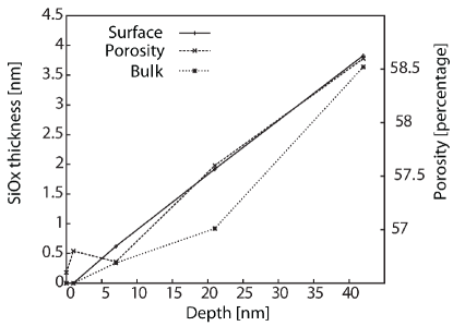
where is the density (mass pr unit volume) of SiO2 and is the formula weight of Si Watts and Wolstenholme (2003). From these equations we calculated the to be 0.61. The thickness of the SiOx was then found for the ten samples, and plotted in Figure 5. The plot shows that there is almost a linear relation of SiOx growth on both surface and bulk PS. The SiOx thickness at the surface PS grows from 0 nm to 3.8 nm during the 42 days. SiOx in the pores of bulk PS however, grows from 0 nm to 3.6 nm. This calculations is based on an oxide on a planer surface. Therefore, with a rough surface, such as for PS, an overestimation of the oxide will be carried out when calculating the SiOx thickness. However, this method of analysis does not take the sub-oxides into account, which in turn will result in a smaller thickness then what is expected.
The calculated oxide thickness is far smaller then what was observed with TEM in Figure 2, which was about 15 nm. If the oxide thickness after ageing was indeed 15 nm, no Si0 peak would be visible in the spectra from this sample. This implies that the SiOx coverage is not uniformly distributed on the PS. The oxide thickness calculated in this paper is therefore the average oxide thickness.
III.4 Refractive index and porosity of the Porous Silicon before and after oxidation.
Figure 6 shows the refractive index with depth in the PS layer at day 1 and day 42. The layers are birefringent, so the refractive indices in both x- and z- (normal to the sample surface) directions are shown. As there is only one axis of anisotropy, the refractive index in the y-direction is identical to the x-direction and is not shown. In both directions, a small reduction in the refractive index is observed from day 1 to day 42.
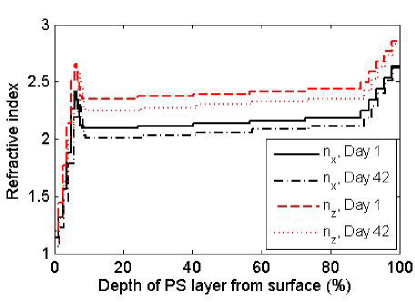
For best possible accordance between SE and XPS, each sample is measured by ellipsometry within day one after etching and then again just before XPS measurements. Comparing the information obtained about oxidation of the PS structures, it is clear that SE is rather insensitive to oxidation in the PS structures. Partly, the inclusion of oxide in the ellipsometry model is complicated by the number of different oxidation states; for most of the samples only a small fraction of the oxidized species is SiO2. It is also possible that an alternative model could give larger deflections with respect to oxygen content. However, when this is said, the marginal difference in and , and consequently in refractive index between day 1 and day 42, indicates that it is a challenge to determine oxidation of PS with SE. It is also rather common to neglect oxidation when performing ellipsometric characterization of PS Selj et al. (2011); Wongmanerod et al. (2001). Whether neglecting SiO2 is a viable approach or not depends, of course on the amount of oxide, but also on the information sought. Obviously, information about the chemical composition of the material is lost, but, on the other hand, changes in the effective refractive index of the material are small. Considering the densities and molecular weights of Si ( = 2330 kg/m3, = 28.0855 g/mol) and SiO2 ( = 2200 kg/m3, = 60.0843 g/mol) it can be seen that for an oxide of thickness t, the fractional consumption of the Si wall is
| (4) |
while the remaining 0.56t is expansion into the pores (26). A locally flat surface, i.e. isotropic expansion through the volume (27), and oxidation by SiO2 only is assumed. The net effect of oxidation can then be thought of as a replacement of a medium consisting of 44 % Si and 56 % air with a medium consisting of 100 % SiO2. In the Bruggeman effective medium model (BEMA), 44 % Si and 56 % air have an effective refractive index, Neff, given by the equation
| (5) |
Inserting the refractive indices NSi(700 nm) = 3.77 and NAir(700 nm) = 1.00, gives an effective refractive index Neff (700 nm) = 2.07. The refractive index of SiO2 at the same wavelength is 1.45, hence the change in effective refractive index of the oxidized area is relatively small. The small reduction in refractive index gives the observed outcome of increased porosity in the ellipsometric modelling. The apparent increase in porosity with ageing is therefore ascribed to an increase in oxide content of the structure. As stated earlier, the oxidation growth is almost linear, this seems also to be the case for the porosity of the PS. The apparent increase in porosity is relatively modest and generates only a small change in the reflectance of these samples. However, adding SiO2 in the ellipsometric modelling does not improve the fit for any of the samples.
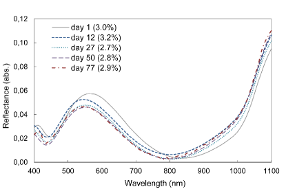
The evolution of the reflectance from a graded PS ARC with ageing is showed in Figure 7. The reflectance integrated over the solar spectrum is shown in parenthesis. Reflectance measurements are performed immediately after fabrication and then with intervals of approximately two weeks. A small wavelength shift and amplitude lowering of the reflectance peak is visible. The uncertainty of the measurements is estimated to be 0.15 % absolute, while the measured effective reflectance of the ARC varies by 0.5 % over time. Therefore, it seems that the ARC experiences small variations in the reflectance with time, but the performance is more inclined towards an improvement than a degradation.
IV Conclusion
During oxidation of the PS elements such as pure Si (Si0), Si2O (Si+), SiO (Si2+), Si2O3 (Si3+), and SiO2 (Si4+) is present. In addition, both hydrogen and carbon is introduced to the PS in the form of Si3SiH and CO. Also, when sputtering the PS with Ar for depth profiling, aSi is created in the structure. This results in an increased FWHM of the Si2p peaks. Ageing the PS results in a linear increase in the average SiOx thickness, which grows from 0 nm to 3.8 nm during the 42 days. Bulk PS however, grows from 0 nm to 3.6 nm. The porosity shows the same trend, with a linear increase in porosity from 56.6 % to 58.6 % with ageing and the increase in SiOx thickness. The reflectance of the multilayer structures is apparently quite robust and not subject to any degradation. If structure and storage conditions are known, the small change in reflectance due to oxidation could be accounted for in the design of the coatings to improve the effective reflectivity further.
References
- Zhang (2004) X. G. Zhang, Journal of The Electrochemical Society 151, C69 (2004).
- Rossow et al. (1995a) U. Rossow, U. Frotscher, M. Thonissen, M. G. Berger, and S. Frohnhoff, Thin Solid Films 255, 5 (1995a).
- Yuan et al. (2009) H. Yuan, V. E. Yost, M. R. Page, P. Stradins, D. L. Meier, and H. Branz, Appl. Phys. Lett. 95, 123501 (2009).
- Kwon et al. (2007) J. Kwon, S. Lee, and B. Ju, J. Appl. Phys. 101, 104515 (2007).
- Lipinski et al. (2003) M. Lipinski, S. Bastide, P. Panek, and C. Levy-Clement, Physica status solidi(a) 197, 512 (2003).
- Yerokhov et al. (2000) V. Yerokhov, I. Melnyk, A. Tsisaruk, and I. Semochko, Opto-elect. rev. 8, 414 (2000).
- Bilyalov et al. (2000) R. Bilyalov, R. Ludemann, W. Wettling, L. Staalmans, J. Poortmans, J. Nijs, L. Schirone, G. Sotgiu, S. S., and C. Levy-Clemet, Solar Energy Materials and Solar Cells 60, 391 (2000).
- Selj et al. (2010) J. H. Selj, A. Thøgersen, S. Foss, and E. Marstein, J. Appl Phys. 107, 074904 (2010).
- Herino et al. (1987) R. Herino, G. Bomchil, K. Barla, C. Bertrand, and J. L. Ginoux, J. Electrochem. Soc. 134 (1987).
- Canham (1997) L. Canham, Properties of Porous Silicon (EMIS Datareviews Series No 18, 1997).
- Grosman and Ortega (2006a) A. Grosman and C. Ortega, Properties of Porous Silicon EMIS Data Reviews Series No 18. (The institution of Electrical Engineers, London, UK, 2006a).
- Grosman and Ortega (2006b) A. Grosman and C. Ortega, Properties of Porous Silicon. (The institution of Electrical Engineers, London, UK, 2006b), p. 145.
- Rao et al. (1990) A. Rao, F. Ozanam, and J.-N. Chazalviel, J. of Elec. Spec. and Rel. Phenom. 54-55, 1215 (1990).
- Domashevskaya et al. (1998) E. Domashevskaya, V. Kashkarov, E. Manukovskii, A. Schukarev, and V. Terekhov, J. of. Elec. Spec. Rel. Phenom. 88, 969 (1998).
- Peden et al. (1993) C. H. F. Peden, J. W. Rogers, N. D. S. Jr., K. B. Kidd, and K. L. Tsang., Phys. Rev. B 47, 15622 (1993).
- Himpsel et al. (1988) F. Himpsel, F. McFeeley, A. Taleb-Ibrahimi, J. Yarmoff, and G. Hollinger., Phys. Rev. B 38, 6084 (1988).
- Thøgersen et al. (2008) A. Thøgersen, S. Diplas, J. Mayandi, T. Finstad, A. Olsen, J. F. Watts, M. Mitome, and Y. Bando, J. of Appl. Phys. 103, 024308 (2008).
- Selj et al. (2011) J. Selj, E. Marstein, A. Thøgersen, and S. Foss, Status Physica Solidi (c) 8, 1860 (2011).
- (19) http://www.casaxps.com.
- Pettersson et al. (1998) L. A. A. Pettersson, L. Hultman, and H. Arwin, Appl. Opt. 37, 4130 (1998).
- Rossow et al. (1995b) U. Rossow, U. Frotscher, M. Thonissen, M. G. Berger, S. Frohnhoff, H. Munder, and W. Richter, Thin Solid Films 255, 5 (1995b).
- Cerofolini et al. (2003) G. F. Cerofolini, C. Galati, and L. Renna, Surf. Interface Anal. 35, 968 (2003).
- Lu et al. (1993) Z. H. Lu, M. Graham, D. Jiang, and K. Tan, Appl. Phys. Lett. 63, 2941 (1993).
- Pleul et al. (2003) D. Pleul, R. Frenzel, M. Eschner, and F. Simon, Anal Bioanal Chem 375, 1276 (2003).
- Wagner et al. (1982) C. D. Wagner, D. E. Passoja, H. F. Hillery, T. G. Kinisky, H. A. Six, W. T. Jansen, and J. A. Taylor, J. Vac. Sci. Technol. A 21, 933 (1982).
- Hollinger et al. (1975) G. Hollinger, Y. Jugnet, P. Pertosa, and T. M. Duc, Chem. Phys. Lett. 36, 441 (1975).
- Yue et al. (1999) Z. Yue, W. Jiang, L. Wang, S. Gardner, and C. P. Jr., Carbon 37, 1785 (1999).
- Guerrero-Lemus et al. (1999) R. Guerrero-Lemus, J. Moreno, R. Martin-Palma, F. Ben-Hander, J. M. Martinez-Duart, J. Fierro, and P. Gomez-Garrido, Thin Solid Films 354, 34 (1999).
- Ley et al. (1982) L. Ley, J. Reichardt, and R. L. Johnson, Phys. Rev. Lett. 49, 1664 (1982).
- Watts and Wolstenholme (2003) J. Watts and J. Wolstenholme, An introduction to Surface Analysis by XPS and AES (WILEY, 2003).
- Wongmanerod et al. (2001) C. Wongmanerod, S. Zangooie, and H. Arwin, Appl. Surf. Sci. 172, 117 (2001).