Composition and structure of Pd nanoclusters in SiOx thin film
Abstract
The nucleation, distribution, composition and structure of Pd nanocrystals in SiO2 multilayers containing Ge, Si, and Pd are studied using High Resolution Transmission Electron Microscopy (HRTEM) and X-ray Photoelectron Spectroscopy (XPS), before and after heat treatment. The Pd nanocrystals in the as deposited sample seem to be capped by a layer of PdOx. A 1-2 eV shift in binding energy was found for the Pd-3d XPS peak, due to initial state Pd to O charge transfer in this layer. The heat treatment results in a decomposition of PdO and Pd into pure Pd nanocrystals and SiO2.
I Introduction
Material systems containing silicon and germanium nanocrystals have attracted much attention due to their optical and electronic properties Agan et al. (2006); Salh et al. (2007), as well as their potential applications in photo detectors Wang et al. (2002a), light emitters Wang et al. (2002b), single electron transistors Averin and Likharev (1986) and non-volatile memories Kanoun et al. (2004). Nanoclusters embedded in a SiO2 matrix is an attractive option towards nanocluster based device development Yang et al. (2005). The most important factors influencing the optical properties of the SiO2-nanocluster devices are size, spatial distribution, atomic and electronic structure as well as the surface properties of the nanoclusters.
Pd is an especially interesting material when used for catalytic converters in auto-mobile technology for the elimination of NOX (Nitrogen Oxides) in the exhaust gases of gasoline engines Kielhorn et al. (2002). Considerable research has also been conducted in the use of Pd catalysts for the combustion of methane. Particle morphology and oxidation state can play an important role in defining the active sites on Pd catalysts. Pd is also found in other applications such as Granular Metal (GM) films, cermets or nano-cermets, where metal particles on MgO cubes Ichinohe et al. (2004). Transition metal particles have interesting properties due to quantum size effect, owing to the dramatic reduction of the number of free electrons Teranishi and Miyake (1998). The nanoparticle matrix may formed advanced material system with new electronic, magnetic, optic, and thermal properties Teranishi and Miyake (1998).
In this work, samples containing both Pd nanocrystals and Ge clusters embedded in SiO2 layers supersaturated with Si, were studied in detail, before and after heat treatment. The formation, composition, distribution, and the atomic and electronic structure of Ge and Pd nanoclusters were studied by High Resolution Transmission Electron Microscopy (HRTEM) and X-ray Photoelectron Spectroscopy (XPS).
II Experimental
The samples were produced by growing a 3 nm layer of SiO2 on a p-type Si substrate by Rapid Thermal Oxidation (RTO) at 1000∘C for 6 sec. Prior to growing the RTO layer the wafers were cleaned using a standard RCA procedure (Radio Corporation of America, industry standard for removing contaminants from wafers) followed by immersion in a 10 % HF solution to remove the native oxide. Then a 10 nm layer of silicon rich oxide (46 at. %) was sputtered from a SiO2:Si composite target onto the RTO-SiO2 and heat treated in a N2 atmosphere at 1000∘C for 30 min, as described in our previous article Thøgersen et al. (2008a, b). A 20nm SiO2 layer containing 0.5 at. % Ge and 0.5 at. % Pd, was then sputtered. This sample is reffered to as the as deposited sample (sample ASD) The heat treated sample (sample HT) was then annealed again at 900∘C in a N2 atmosphere for 30 minutes to nucleate Ge and Pd nanocrystals. Cross-sectional TEM samples were prepared by ion-milling using a Gatan precision ion polishing system with a 5 kV gun voltage.
The nanocrystals were studied with HRTEM using a 300 keV JEOL 3100FEF TEM with an Omega imaging filter. Additional HRTEM images were acquired using a 200 keV JEOL 2010F TEM. XPS was performed in a KRATOS AXIS ULTRADLD using monochromatic Al K radiation ( eV) on plane-view samples using 0∘ angle of emission (vertical) and charge compensation with ion energy electrons from a flood gun. The X-ray source was operated at 10 mA and 15 kV. The inelastic mean free path of the Ge3d electrons in SiO2 is 3.9 nm Moulde et al. (1992); NIST (2009). Emission normal to the surface results in a photoelectron escape depth of 11.8 nm NIST (2009), which allowed us to study the silicon nanoclusters located 11.8 nm below the surface of the oxide. Accordingly the inelastic mean free path of the Pd-3d electrons in SiO2 is 3.38 nm, which allows us to study Pd nanocrystals within an analysis depth of 10.1 nm. The spectra were peak fitted using the CasaXPS program http://www.casaxps.com/ after subtraction of a Shirley type background. The spectra were calibrated by adjusting peak positions of the O-1s and Si-2p signals from SiO2 at 533 eV and 103.6 eV respectively, and the Si-2p from the Si substrate at 99.5 eVMoulde et al. (1992). Composition depth profile was performed with Ar ion etching, on a 3x3 mm spot area, at 2 kV, 100 A current and a cycle time of 20 s.
III Results and Discussion
Nanoclusters of different sizes in various layers were observed in both the as deposited (ASD) and heat treated sample (HT), see Figure 1. Dark Ge and Pd nanoclusters are visible in the SiO2-Ge-Pd layer, 10 nm from the outermost surface (SiO2/glue interface) and 13 nm from the Si substrate. Lattice fringes can be seen in the largest nanoclusters, indicating that many of them are crystalline. The average nanocluster size for sample HT and ASD is 4 nm and 2.5 nm, respectively . Smaller (1-2 nm) clusters are visible in the SiO2-Si layer 6 nm from the Si substrate in sample HT. No lattice fringes were observed in these nanoclusters, indicating an amorphous structure. Since Si has almost no contrast when embedded in SiO2, these nanoclusters contain either Pd or Ge.
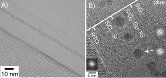
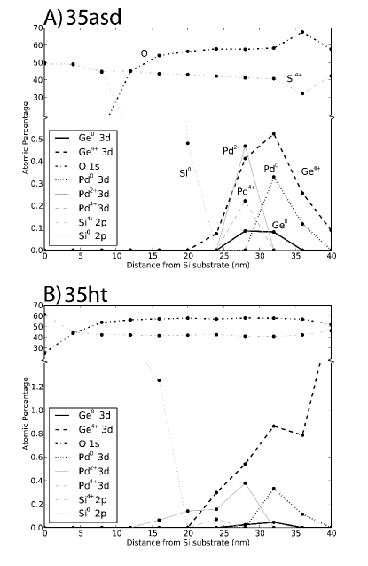
Figure 2 shows the high resolution Si2p, Ge3d, and Pd3d XPS spectra acquired during depth profiling with Ar+ sputtering of samples HT and ASD. The XPS spectra of sample HT show that Ge is distributed wider in the SiO2-Ge-Pd layer, compared to sample ASD, where Ge is located in a narrow band. In addition, Ge surface segregation seems to occur upon annealing in accordance with previous work by Agan et al. Agan et al. (2006) and Marstein et al. /citemarstein:1. Sample ASD looks very similar to sample HT, apart from the location of the Si and Ge (see Figure 2). The Pd distribution is almost the same in both samples. As seen in Figure 1, small nanoclusters were observed in the SiO2-Si layer of samples HT. The Ge-3d and Pd-3d spectra of sample HT show very little or no increase in the Ge and Pd concentration in the SiO2-Si layer. This indicates that the nanoclusters shown in Figure 1 that are present in the SiO2-Si layer, have diffused to this area during electron beam exposure. There is a visible shift in the position of the Pd peaks with the depth in sample ASD. This shift, not seen in sample HT, will be discussed in Section V.2. Figure 4 shows the elemental distribution with depth for sample ASD and HT. The quantification is based upon peak fitting, being shown in more in the following sections.
The results of the as deposited samples are more complicated to interpret. We therefore present first the less complicated results of the heat treated samples, followed by the as deposited ones.

IV Results and Discussion: Heat treated samples
The composition of the heat treated samples measured with XPS, EELS, EFTEM and EDS is presented in Section IV.1, while the atomic structure found by TEM is presented in Section IV.2.
IV.1 Nanocluster composition
XPS was used to identify the chemical state of different elements present in sample HT. Figure 3B and D shows the fitted XPS spectrum of the Pd-3d and Ge-3d peak. The measured binding energies of the two Ge peaks were 29.8 eV and eV, with an energy separation eV. The literature binding energy value for pure Ge is 29.4 eV Moulde et al. (1992) and 32.5 eV for GeO2 Wu et al. (2002). The Ge-3d energy separation/chemical shift between Ge0 and GeO2 is reported to be 3.3 eV NIST (2009). The chemical shift is less susceptible to energy referencing when the same reference is used and both peaks defining the chemical shift exist in the same spectrum. Therefore the above data suggests that the peak at 29.8 corresponds to pure Ge, while the peak at 33.1 eV and eV is from GeO2.
The XPS spectrum in Figure 3B shows the Pd-3d peak. The spectrum is fitted with six components. The two peaks located at binding energies of 348.9 eV and 345.9 eV belong to Ge-LMM. The remaining four peaks may be contributions from Pd and Pd. The measured binding energies are presented in Table 2, and the chemical shifts in Table 3. Pure Pd has a binding energy of 340.4 eV (3d3/2) and 335.1 eV (3d5/2) Moulde et al. (1992), PdO of 341.6 eV (3d3/2) and 336.3 eV (3d5/2), and PdO2 of 343 eV (3d3/2) and 337.9 eV (3d5/2) Kim et al. (1974). The reference values show chemical shifts for the Pd2+-Pd0=1.2 eV, and for Pd4+-Pd0=2.6 eV.
The two smallest peaks in Figure 3B at 341.6 eV and 336.3 eV fit well with PdO, while the larger peaks at 340.1 eV and 334.8 eV correspond to pure Pd. This is in agreement with the chemical shift of 1.5 between the Pd2+-Pd0 of both the 3d3/2 and 3d5/2 peaks. The Pd0 peaks were fitted using slightly asymmetric components, with a FWHM of about 1 eV. These XPS results are shown and discussed in Section V.2 and V.3.
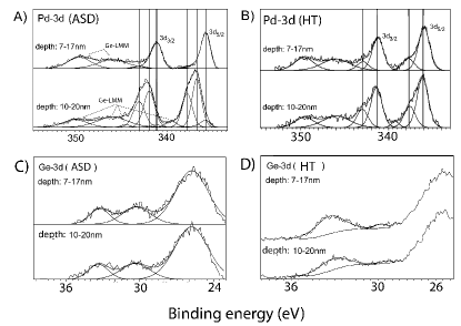
Figure 2 shows significant differences in the Si4+/Si0 intensity ratio in the SiO2-Si layer between the two samples. The increased Si4+/Si0 intensity ratio in the SiO2-Si zone as well as in the Si substrate of the annealed sample is attributed to oxidation upon annealing. This oxidation may also be responsible for the small decrease in pure Ge concentration, as seen in Figure 4.
IV.2 Atomic structure of the nanocrystals
| Sample | Observed | Pd Owen and Yates (1933) | Pd3O4 Meyer and Mueller-Buschbaum (1979) | PdO Christy and Clark (1995) | Pd2Si Nylund (1966) |
|---|---|---|---|---|---|
| d-value | (nm) | (nm) | (nm) | (nm) | |
| (nm) | |||||
| HT | 0.198 | 0.195 | |||
| ASD | 0.226 | 0.224 | |||
| ASD | 0.210 | 0.204 | 0.211 | 0.211 |
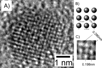
The atomic structure of the nanocrystals in sample HT were studied by Fast Fourier Transform (FFT) patterns. FFT patterns of the Si substrate and two nanocrystals are presented as insets in Figure 1. The FFT of the Si substrate is used as a reference, since the Si unit cell dimensions are known ( nm). The FFT of the two nanocrystals yielded a d-value of nm. The HRTEM image shown in Figure 1 shows a squared pattern with the same lattice plane spacing of nm. The measured d-values as well as references are presented in Table 1. Pure Pd has a Fm-3m space group, with lattice parameter 0.389 nm. The largest d-value is (200): 0.195nm Owen and Yates (1933). This fits well with the measured d-values.
V Results and Discussion: As deposited samples
The composition and atomic structure of sample ASD is presented in the following sections. XPS measurements of sample ASD is presented in Section V.2, and the discussion of the results in in Section V.3.
V.1 Nanocluster composition and atomic structure
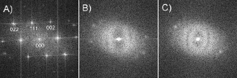
A HRTEM image of a Pd nanocrystal in sample ASD is presented in Figure 5. FFT patterns from the Si substrate and from two nanocrystals are presented in Figure 6. FFT patterns of three different nanocrystal areas in sample ASD yielded the measured d-values of nm, nm, and nm. The experimentally observed d values are then compared to reference values (presented in Table 1). The d-values measured on the three nanocrystal areas in sample ASD fit with Pd3O4, PdSi, Pd2Si, PdO, and pure Pd.
Voogt et al. Voogt et al. (1996) studied PdO particles with a metallic Pd core. The surface tension of PdO is lower than the surface tension of pure metallic Pd, and upon annealing Pd will not dissolve in PdO Voogt et al. (1996). It is therefore reasonable to find particles containing, a metallic core and an oxide skin when heat treated at higher temperatures, because the migration of atoms is relatively easy. During heat treatment this core will grow linearly proportional to the surface area, transforming to Pd and SiOx towards reaching thermodynamic equilibrium. This may explain why we see more Pd oxide in the as deposited samples.
It is therefore reasonable for the Pd nanocrystals in the as deposited samples to have a few atomic layers of PdO and/or Pd2Si around them. During heat treatment, these compounds will react to form pure Pd and SiO2. XPS results of these samples is shown and discussed in the next section.
The HRTEM and XPS of the as deposited and heat treated sample shows that Ge and Pd behave in an opposite manner. After annealing, Pd decomposes into pure Pd and SiO2, whereas Ge oxidises. This may be influenced by residual oxygen in the annealing ambient. The differences in oxidation may also be due to oxygen transfer from Pd to Ge (and Si), as a result of differences in the enthalpy.
V.2 Pd-3d binding energy shifts
| Peak | Sample ASD | Sample HT | References 111Reference Moulde et al. (1992)222Reference Kim et al. (1974) |
|---|---|---|---|
| EB (eV) | EB (eV) | EB (eV) | |
| Pd0-3d3/2 | 341.0 | 340.1 | 340.4 |
| Pd0-3d5/2 | 335.7 | 334.8 | 335.1 |
| Pd2+-3d3/2 | 341.9 | 341.6 | 341.6 |
| Pd2+-3d5/2 | 336.8 | 336.3 | 336.3 |
| Pd4+-3d3/2 | 343.0 | 343.0 | |
| Pd4+-3d5/2 | 337.9 | 337.9 |
The Pd-3d and Ge-3d spectra from sample ASD are shown in Figure 3A and C, while the Pd-3d spectra from sample HT are shown in Figure 3B and D. The experimental binding energies, chemical shifts and reference values are shown in Table 2 and Table 3. We observe a shift in the Pd-3d binding energy with depth in the as deposited sample compared to the heat treated one (Figure 3). The chemical shift is defined as the binding energy difference 3d- 3d. HRTEM image of samples ASD shown in the previous section gave d-values which match well with Pd3O4 (Pd+4 and Pd+2), PdSi (Pd+4), Pd2Si (Pd+2), PdO (Pd+2), and pure Pd (Pd0).
The Pd-3d peak for sample ASD is visible at sample depth range of 7-17 nm and 10-20 nm, due to a 10 nm photoelectron escape depth for Pd in SiO2. The depth was determined using the Si-2p peak from the Si substrate and the photoelectron escape depth. The spectrum at 7-17 nm is from the top of the band of Pd nanocrystals, and the spectrum at 10-20 nm is from the bottom.
The Pd-3d spectra of both samples at a depth of 7-17 nm show four peaks in addition to the peaks belonging to Ge-LMM. Figure 2 shows the Si-2p peaks of sample ASD. Only Si from SiO2 (Si4+) was detected at either depths. This in combination with the Pd peaks means that Pd2Si and PdSi are not present in the samples. The smaller peaks in Figure 3 A must therefore result from PdO and/or Pd3O4.
The chemical shift between the two 3d3/2 and 3d5/2 peak maxima in Figure 3 A at a depth of 7-17 nm are 2 eV and 2.2 eV respectively for sample ASD. The chemical shift values are higher than the expected one for Pd2+ (1.2 eV) and lower than the one expected for Pd4+ (2.6 eV Kim et al. (1974); Moulde et al. (1992)). A reduced chemical shift could be attributed to the presence of Pd2+/Pd4+ mixed valency. Pd3O4 contains a mixed valency of two Pd2+ and one Pd4+ ions. The peaks at 343 eV and 337.9 eV most probably are due to the presence of Pd3O4.
| Sample | Chem. shift: | 3d3/2 | 3d5/2 |
| () | (eV) | (eV) | |
| ( 0.14 eV) | ( 0.14 eV) | ||
| HT | Pd+2- Pd0 | 1.5 | 1.5 |
| ASD | Pd+2- Pd0 | 0.9 | 0.9 |
| ASD | Pd+4- Pd0 | 2 | 2.2 |
| reference Moulde et al. (1992) | Pd0-Pd+2 | 1.2 | 1.2 |
| reference Kim et al. (1974) | Pd0-Pd+4 | 2.6 | 2.8 |
The Pd-3d spectra from a depth of 10-20 nm in sample ASD contain six compounds in addition to the Ge-LMM peaks. The two largest compounds were fitted with a pure Gaussian peak. The chemical shift between the largest compounds and the Pd0 peaks is 0.9 eV for both the 3d3/2- and 3d5/2- peak in sample ASD. These peaks can probably be assigned to a Pd2+ peak (PdO or PdOx).
Figure 3 shows that pure Pd is mostly found in the upper part of the nanocluster band, while the (sub)oxides were found in the lowest part of the nanocluster band, either as an oxide skin around the Pd nanocrystals and / or as pure oxide nanocrystals. This inhomogenity has most probably occurred during sputtering deposition. A small shift to a higher binding energy is observed for both Pd0 (1 eV) and Pd2+ peaks (0.5-0.7 eV) as compared to the reference values Kim et al. (1974); Moulde et al. (1992). The chemical shift between Pd2+ and Pd0 is lower than the reference values and lower than what was found in sample HT. This will be discussed in the next section.
V.3 The nature of the Pd-3d binding energy shift
In a previous paper, we studied the binding energy shifts of Er2O3 nanoclusters in SiO2, and the various factors influencing the binding energy were discussed in detailThogersen et al. (2009). In this work we performed a similar study on Pd nanoclusters in SiO2 in order to evaluate the decrease in chemical shifts found in the as deposited sample as compared to the heat treated sample. Shifts in binding energy can be expressed as
| (1) |
In the above equation, is a measure of the Coulomb interaction between the valence and core electrons, and expresses changes in the valence charge. reflects therefore charge transfer effects. is the contribution of the changes in Madelung potential. contains changes in energy referencing, including variations of the sample work function and of the energy of charge compensating electrons, which may be important in the case of insulators. The first two terms in Equation 1 refer to initial state effects, while the third term expresses the dependence of on energy referencing in the case of insulators. The fourth term is the contribution of the relaxation energy , which is the kinetic energy gained (negative sign) when the electrons in the solid screen the photohole produced by the photoemission process; this is a final state effect.
A 1-2 eV core level shift to higher in the Pd-3d peak was observed in the work by Ichinohe et al. Ichinohe et al. (2004), who studied Pd clusters in SiO2. The shift was attributed to final state effects as a consequence of the decrease in particle size, which is an initial state effect, and a subsequent decrease in screening. This demonstrates how the initial state influences the final state effects. In the case of nanoclusters in an insulating matrix, the core hole relaxation, screening could contain matrix contributions to some extent. Since Pd is a metal, it is characterized by a large screening efficiency. SiO2, on the other hand, is an insulator and has a low screening efficiency. Therefore, assuming an external screening contribution by SiO2, the screening in bulk Pd is higher than the screening in Pd nanocrystals embedded in SiO2, due to the low screening contribution from the oxide. Quantum confinement effects and an increased band gap may also reduce screening since the core hole screening by the conduction band depend on the band gap. The larger the band gap is the lower the screening efficiency becomes. A reduction in core hole screening appears as an increase in binding energy.
The (sub)oxide in the as deposited samples has a decreased chemical shift compared to the heat treated samples. PdO has a higher dielectric constant than its surrounding SiO2 matrix similarly to Er2O3 in the same matrix Thogersen et al. (2009). In accordance with the previous argumentation Thogersen et al. (2009), the screening contribution of the surrounding SiO2 on the Pd and PdO clusters is expected to be small. Considering absence of energy referencing issues, initial state effects seem to have a dominant role in the increase of the binding energy of Pd nanocrystals and PdOx clusters. As for the Er2O3 nanoclusters Thogersen et al. (2009), charge transfer from Pd to O can lead to the creation of positive surface charges. The increased binding energy may therefore be due to initial state effects, such as charge transfer from Pd towards the interface. The smaller the nanocluster size, the higher the surface/volume ratio. Therefore interfacial transport phenomena are more enhanced. Variations in the effectiveness of charge neutralization on Pd nanocrystals with and without a PdOx skin may also account for differences in peak shifts.
VI Conclusion
Multilayer samples containing Pd, Ge and Si were made in order to study the nucleation, distribution, composition as well as atomic and electronic structure of Ge and Pd nanoclusters. The nanocrystals were observed by HRTEM, EDS and EFTEM imaging. Ge was observed in the form of small amorphous nanoclusters. The as deposited samples contained not only pure Pd nanocrystals, but also Pd-oxides. A 1-2 eV shift in binding energy found for the XPS Pd-3d peak of pure Pd and Pd2+ was attributed to initial state effects arising from an increased charge transfer from Pd to O in the nanocrystals and / or to electrostatic charging. According to the combined TEM and XPS data, the Pd nanoclusters in the as deposited samples consist of Pd and PdOx.
References
- Agan et al. (2006) S. Agan, A. Dana, and A. Aydinli, J. Phys.: Condens. Matter 18, 5037 (2006).
- Salh et al. (2007) R. Salh, L. Fitting, E. V. Kolesnikova, A. A. Sitnikova, M. V. Zamoryanskaya, B. Schmidt, and H.-J. Fitting, Semiconductors 41, 387 (2007).
- Wang et al. (2002a) K. L. Wang, J. L. Liu, and G. Jin, J. Cryst. Growth 237-239, 1892 (2002a).
- Wang et al. (2002b) Y. Q. Wang, G. L. Kong, W. D. Chen, H. W. Diao, C. Y. Chen, S. B. Zhang, and X. B. Liao, Appl. Phys. Lett. 81, 4174 (2002b).
- Averin and Likharev (1986) D. V. Averin and K. K. Likharev, J. Low-Temp. Phys. 77, 2394 (1986).
- Kanoun et al. (2004) M. Kanoun, , A. S. A. Baron, and F. Mazen, Appl. Phys. Lett. 84, 5079 (2004).
- Yang et al. (2005) Y. M. Yang, X. L. Wu, L. W. Yang, G. S. Huang, G. G. Siu, and P. K. Chu, J. Appl. Phys. 98, 064303 (2005).
- Kielhorn et al. (2002) J. Kielhorn, C. Melber, D. Keller, and I. Mangelsdorf, International Journal of Hygiene and Environmental Health 205, 417 (2002).
- Ichinohe et al. (2004) T. Ichinohe, S. Masaki, K. Uchida, S. Nozaki, and H. Morisaki, Thin solid films 466, 27 (2004).
- Teranishi and Miyake (1998) T. Teranishi and M. Miyake, Chem. Mater. 1998 10, 594 (1998).
- Thøgersen et al. (2008a) A. Thøgersen, J. Mayandi, J. S. Christensen, T. Finstad, M. Mitome, Y. Bando, and A. Olsen, J. Appl. Phys. 104, 094315 (2008a).
- Thøgersen et al. (2008b) A. Thøgersen, S. Diplas, J. Mayandi, T. Finstad, A. Olsen, J. F. Watts, M. Mitome, and Y. Bando, J. Appl. Phys. 103, 024308 (2008b).
- Moulde et al. (1992) J. F. Moulde, W. F. Stickle, P. E. Sobol, and K. D. Bomben, Handbook of X-Ray Photoelectron Spectroscopy (Perkin-Elmer Corporation, 1992), p. 201.
- NIST (2009) NIST, http://srdata.nist.gov/xps/ (2009).
- (15) http://www.casaxps.com/.
- Wu et al. (2002) X. Wu, M. Lu, and W. Yao, Surf. and Coat. Tech. 161, 92 (2002).
- Kim et al. (1974) K. Kim, A. Gossmann, and N. Winograd, An. Chem. 46, 197 (1974).
- Owen and Yates (1933) E. Owen and E. Yates, Phil. Mag. 15, 472 (1933).
- Meyer and Mueller-Buschbaum (1979) H. J. Meyer and H. Mueller-Buschbaum, Zeitschrift fuer Naturforschung, Teil B. Anorganische Chemie, Organische Chemie (33,1978-41,1986) 34, 1661 (1979).
- Christy and Clark (1995) A. G. Christy and S. M. Clark, Physical Review, Serie 3. B - Condensed Matter (18,1978-) 52, 9259 (1995).
- Nylund (1966) A. Nylund, Acta Chemica Scandinavica 20, 2381 (1966).
- Voogt et al. (1996) E. Voogt, A. Mens, O. Gijzeman, and J. Geus, Surf. Sci. 350, 21 (1996).
- Thogersen et al. (2009) A. Thogersen, J. M. A. Finstad, A. Olsen, S. Diplas, M. Mitome, and Y. Bando, J. of Appl. Phys. 106, 014305 (2009).