Electronic and crystalline structures of zero band-gap PdLuBi thin films grown epitaxially on MgO(100)
Abstract
Thin films of the proposed topological insulator PdLuBi - a Heusler compound with the structure - were prepared on Ta-Mo-buffered MgO(100) substrates by co-sputtering from PdBi2 and Lu targets. Epitaxial growth of high-quality PdLuBi films was confirmed by X-ray spectrometry and reflection high-energy electron diffraction. The root-mean-square roughness of the films was as low as 1.45 nm, although the films were deposited at high temperature. The film composition is close to the ideal stoichiometric ratio. The valence band spectra of the PdLuBi films, observed by hard X-ray photoelectron spectroscopy, correspond perfectly to the ab-initio-calculated density of states.
Zero energy consumption in electron transport, spin channel splitting, protection of spins from thermal activity, and other interesting, recently proposed, physical properties in topological insulators (TIs) would greatly improve the performance of semiconductor devices, achieve spin control in spintronics devices without application of magnetic fields, and provide an excellent platform for the application of quantum physics, e.g., quantum computers Kane and Mele (2005); Bernevig, Hughes, and Zhang (2006); Qi, Hughes, and Zhang (2008); Konig et al. (2007). Until now, most studies of TIs have focused on HgTe/CdTe/HgTe quantum wells with two-dimensional (2D) topological states Konig et al. (2007) and three-dimensional (3D) TIs, Bi1-xSbx, Bi1-xTex, and Sb1-xTex Fu, Kane, and Mele (2007); Zhang et al. (2009); Chen et al. (2009). Electrical properties related to the quantum spin Hall effect have only been observed in HgTe/CdTe/HgTe quantum wells, which have been fabricated by molecular beam epitaxy and used as rudimentary devices. Even for HgTe/CdTe/HgTe quantum wells, the difficult and expensive fabrication of the devices has impeded further study. In order to resolve this problem, we suggest a new platform based on half-Heusler compounds for the study of TIs Chadov et al. (2010). A band gap arises in half-Heusler compounds when the total number of valence electrons equals 18 as a result of a closed-shell electronic configuration Jung, Koo, and Whangbo (2000), although the material consists of three metals. The and bands are inverted in some semiconducting Heusler compounds with heavy elements as a result of strong spin–orbit coupling Chadov et al. (2010); Xiao et al. (2010). This leads to a TI state with a zero band gap that can be used in 2D TI quantum well structures. Considering the large range of lattice constants corresponding to the variety of materials and the easy fabrication conditions of Heusler compounds, we suggest that TI devices with Heusler compounds may become feasible for applications. For this purpose, high-quality epitaxial PdLuBi films were fabricated by co-sputtering.
Samples with the structures MgO(100)/Mo (2 nm)/Ta (20 nm)/Mo (1 nm)/ PdLuBi (40 nm)/MgO (17 nm) were prepared by direct-current magnetron co-sputtering under an Ar atmosphere. The base pressure of the sputtering chamber was below Pa. The angle of inclination between each target and the substrate was about and the distance between the sources and target was about 7.95 inches. The substrate was rotated during film growth. The composition of the PdLuBi thin film was analyzed by Rutherford backscattering spectrometry and particle-induced X-ray emission. The crystalline structure was examined by X-ray diffraction (D8-Discover, Bruker AXS Inc.). The surface morphologies of the films were analyzed in situ using reflection high- energy electron diffraction (RHEED, STAIB Instrument Inc.). Ex situ surface analysis was carried out using atomic force microscopy (5600LS, Agilent Technologies Inc.). The valence band spectra of the PdLuBi films were observed using hard-X-Ray photoelectron spectroscopy (HAXPES) at BL47XU of Spring-8 (Japan). For details of the HAXPES experiments, see References Fecher et al. (2008); Ouardi et al. (2011a); Kozina et al. (2011).
Mo and Ta layers were deposited at C, and then annealed at C. The Mo layer was used to induce growth of Ta(100) on MgO(100) instead of Ta(110). After this process, a single-crystalline film of Ta–Mo(100) was built on MgO(100) with a in-plane rotation. Because Mo and Ta can be miscible with each other at high temperatures, the lattice constant of Ta–Mo can be tuned by precise adjustment of the composition. In this study, the lattice constant of PdLuBi was slightly smaller than twice the lattice constant of Ta. A thin Mo layer was therefore used between the Ta and PdLuBi layers. The root-mean-square roughness of the Ta–Mo layer was below 3 Å. The PdLuBi layer was deposited at C. To obtain a semiconducting Heusler film of high quality, a high substrate temperature is usually necessary. However, as a result of the low bonding energy between Bi atoms, Bi almost disappears above a substrate temperature of C when the film is sputtered from three separate targets. On the other hand, the melting point of PdBi2 (C) is much higher than that of Bi (C), implying a higher bonding energy of Pd–Bi. Bi was therefore sputtered from a PdBi2 target to reduce the problem of Bi loss at high growth temperatures. In this case, the composition ratio of Pd:Bi could be tuned using the annealing temperature and the composition ratio of Lu:Pd could be tuned using the sputtering power. Using this procedure, films with a composition ratio of Pd:Lu:Bi = 33.5:33.4:33.1 (at%; %) were obtained at C.
Figure 1 shows the X-ray diffraction pattern of a PdLuBi thin film on Ta–Mo-buffered MgO(100). Only the (200) and (400) diffraction peaks of the PdLuBi film are observed in the (100) polar -scan (see 1(a)). The lattice constant of the PdLuBi film is Å and corresponds to that reported for the bulk material Hasse et al. (2002). The (111) polar scan and the azimuth -scan of the PdLuBi(111) diffraction peak (inset of 1(b)) with four-fold symmetry prove epitaxial growth of the PdLuBi film.
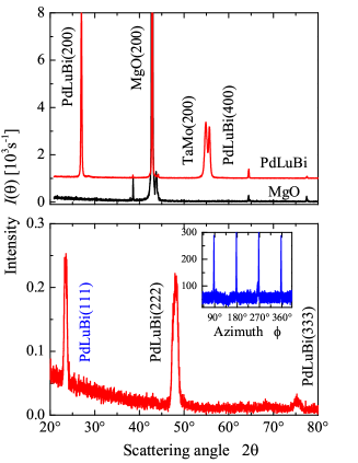
(a) (100) polar scan of PdLuBi (red curve); the black solid curve indicates the background from the MgO(100) substrate. (b) (111) polar scan of PdLuBi and azimuth scan of PdLuBi(111) (inset).
The surface morphology of the film is shown in Figure 2(a). The root-mean-square roughness is around 1.45 nm, although the film was deposited at C. The RHEED pattern of the PdLuBi film without a cap layer is shown in Figure 2(b). It is known that single-crystalline films with an atomically flat 2D surface produce a stripe pattern, whereas single-crystalline films with an atomically rough (3D) surface produce a transmission pattern, i.e., a set of broad spots Ichimiya and Cohen (2004). Polycrystalline films and textured films without in-plane orientation form a set of concentric circles instead. It is clear from Figure 2 that a spotty pattern was observed. This indicates that a single-crystalline PdLuBi film with an atomically rough surface—either via a 3D island (Volmer–Weber) growth mode or a layer-plus-island (Stranski–Krastanov) growth mode—was obtained successfully.
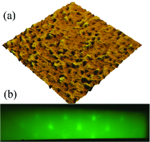
(a) Atomic force microscopy three-dimensional surface representation of PdLuBi with cap layer, (b) reflection high-energy electron diffraction pattern of PdLuBi.
The electronic structure of PdLuBi was calculated using Wien2k Blaha et al. (2001). More details are given in Reference Ouardi et al. (2010). Spin–orbit interactions were included for all atoms and LDA with the self- interaction correction double-counting scheme for Lu. An effective Coulomb energy of Ry was used to reproduce the measured energy of the Lu doublet; Å was found for the relaxed lattice parameter. The result of the electronic structure calculations is shown in Figure 3. The compound turns out to be similar to a zero band gap semiconductor (compare Ouardi et al. (2011b); Shekhar et al. (2012) and references there). The optical gap at is closed. The valence and conduction bands have a small overlap of about 130 meV. A fraction of about electrons is found in the conduction band. This situation may change for slightly smaller lattice parameters (see Figure 3(c)) or a slight tetragonal distortion. Both effects are principally able to open up the band gap again at (compare also Reference Xiao et al. (2010)). A slight tetragonal distortion may particularly occur in thin films with pseudomorphic growth.

(a) shows the complete band structure for the relaxed lattice parameter. (b) and (c) show the band structure in the vicinity of the Fermi energy for the thin film lattice parameter and a 5% compressed lattice parameter, respectively. In (c), a small band gap of width 40 meV is opened. Calculations were performed with spin–orbit interactions for all elements and LDA for the Lu electrons.
Valence band spectra of PdLuBi are presented in Figure 4 and compared to the calculated density of states. Figure 4(a) shows the valence band spectra excited by photons of energy about 8 keV. The high intensity with a maximum between -12.5 and -11 eV corresponds to excitation of the low-lying Bi states with symmetry, as is seen by comparison with the density of states. The Lu - spin–orbit doublet is found at energies of eV and eV, with a spin–orbit splitting of eV. The Lu states reside on top of the states from the MgO protective overlayer that usually appear at about -9 eV. Such MgO states were previously also observed in the spectra from MgO-covered Co2MnSi Fecher et al. (2008). The upper part of the valence spectra above -6.5 eV exhibits the typical structure of the PdLuBi valence bands with four major maxima (-6, -5.16, -4.31, -2.1 eV) and a smaller one at -2.9 eV. The splitting of the states at about -4 eV is not resolved in the spectrum. Slight energy differences between the maxima in the density of states and maxima of the spectrum are observed. These energy shifts are larger for states further away from the Fermi energy (for example 0.3 eV at the -2.1 eV maximum and 0.6 eV at the -5.16 eV maximum). This is a typical effect of the photoemission process and emerges from the complex self-energy of the photoelectrons interacting with the remaining electron system. The spectra exhibit no clear cut-off at the Fermi energy as is observed when a metallic-type density is terminated by the Fermi–Dirac distribution, but a rather smooth, linearly decreasing intensity is observed. A similar behavior was found in bulk materials of the zero band gap Heusler compounds PtYSb Ouardi et al. (2011b) and PtLuSb Shekhar et al. (2012). A splitting of the La states was reported for thin PtLaBi films grown on YAlO3(001) by three-source magnetron co-sputtering Miyawaki et al. (2012). The appearance of the satellite peaks is explained as being the result of charge transfer, as appears, for example, in oxides. The PdLuBi films reported here did not exhibit any additional splitting of core levels, which also indicates their high quality with respect to impurities, structure, and composition.
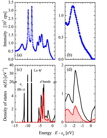
(a)–(b) show the valence band spectra taken with a photon energy of about 8 keV. (c)–(d) show the density of states, and the density localized at the Pd atoms is marked by the shaded area. (b) and (d) show the valence band close to the Fermi energy on an enlarged scale.
In summary, high-quality epitaxial thin films of the Heusler TI PdLuBi were successfully prepared. The composition of Pd:Lu:Bi in the film grown at C is stoichiometric, with ratios of 1:1:1. The valence band spectra of thin PdLuBi films observed by HAXPES perfectly match the density of states from first principles calculations. PdLuBi has a similar band structure to that of HgTe and thus may be used for the construction of 2D TI quantum well structures.
Acknowledgements.
Financial support by the DFG-JST (projects P 1.3-A and P 2.3-A in research unit FOR 1464 ASPIMATT) is gratefully acknowledged. HAXPES was performed at BL47XU of SPring-8 with approval of JASRI (Proposal No. 2012A0043).References
- Kane and Mele (2005) C. L. Kane and E. J. Mele, Phys. Rev. Lett. 95, 146802 (2005).
- Bernevig, Hughes, and Zhang (2006) B. A. Bernevig, T. L. Hughes, and S. C. Zhang, Science 314, 1757 (2006).
- Qi, Hughes, and Zhang (2008) X. Qi, T. L. Hughes, and S. C. Zhang, Phys. Rev. B 78, 195424 (2008).
- Konig et al. (2007) M. Konig, S. Wiedmann, C. Brune, A. Roth, H. Buhmann, L. W. Molenkamp, X. L. Qi, and S. C. Zhang, Science 318, 766 (2007).
- Fu, Kane, and Mele (2007) L. Fu, C. L. Kane, and E. J. Mele, Phys. Rev. Lett. 98, 106803 (2007).
- Zhang et al. (2009) H. J. Zhang, C. X. Liu, X. L. Qi, X. Dai, Z. Fang, and S. C. Zhang, Nature Phys. 5, 438 (2009).
- Chen et al. (2009) Y. L. Chen, J. G. Analytis, J. H. Chu, Z. K. Liu, S. K. Mo, X. L. Qi, H. J. Zhang, D. H. Lu, X. Dai, Z. Fang, S. C. Zhang, I. R. Fisher, Z. Hussain, and Z. X. Shen, Science 325, 178 (2009).
- Chadov et al. (2010) S. Chadov, X. L. Qi, J. Kübler, G. H. Fecher, C. Felser, and S. C. Zhang, Nature Mat. 9, 541 (2010).
- Jung, Koo, and Whangbo (2000) D. Jung, H. J. Koo, and M. H. Whangbo, J. Mol. Struct. Theochem. 527, 113 (2000).
- Xiao et al. (2010) D. Xiao, Y. Yao, W. Feng, J. Wen, W. Zhu, X.-Q. Chen, G. M. Stocks, and Z. Zhang, Phys. Rev. Let. 105, 096404 (2010).
- Fecher et al. (2008) G. H. Fecher, B. Balke, A. Gloskowskii, S. Ouardi, C. Felser, T. Ishikawa, M. Yamamoto, Y. Yamashita, H. Yoshikawa, S. Ueda, and K. Kobayashi, Appl. Phys. Lett. 92, 193513 (2008).
- Ouardi et al. (2011a) S. Ouardi, G. H. Fecher, X. Kozina, G. Stryganyuk, B. Balke, C. Felser, E. Ikenaga, T. Sugiyama, N. Kawamura, M. Suzuki, and K. Kobayashi, Phys. Rev. Lett. 107, 036402 (2011a).
- Kozina et al. (2011) X. Kozina, G. H. Fecher, G. Stryganyuk, S. Ouardi, B. Balke, C. Felser, G. Schönhense, E. Ikenaga, T. Sugiyama, N. Kawamura, M. Suzuki, T. Taira, T. Uemura, M. Yamamoto, H. Sukegawa, W. Wang, K. Inomata, and K. Kobayashi, Phys. Rev. B 84, 054449 (2011).
- Hasse et al. (2002) M. G. Hasse, T. Schmidt, C. G. Richter, H. Block, and W. Jeitschko, J. Solid State Chem. 168, 18 (2002).
- Ichimiya and Cohen (2004) A. Ichimiya and P. I. Cohen, Reflection High Energy Electron Diffraction (Cambridge University Press, Cambridge, UK, 2004).
- Blaha et al. (2001) P. Blaha, K. Schwarz, G. K. H. Madsen, D. Kvasnicka, and J. Luitz, WIEN2k, An Augmented Plane Wave + Local Orbitals Program for Calculating Crystal Properties (Karlheinz Schwarz, Techn. Universität Wien, Wien, Austria, 2001).
- Ouardi et al. (2010) S. Ouardi, G. H. Fecher, B. Balke, X. Kozina, G. Stryganyuk, C. Felser, S. Lowitzer, D. Ködderitzsch, H. Ebert, and E. Ikenaga, Phys. Rev. B 82, 085108 (2010).
- Ouardi et al. (2011b) S. Ouardi, C. Shekhar, G. H. Fecher, X. Kozina, G. Stryganyuk, C. Felser, S. Ueda, and K. Kobayashi, Appl. Phys. Lett. 98, 211901 (2011b).
- Shekhar et al. (2012) C. Shekhar, S. Ouardi, G. H. Fecher, A. K. Nayak, C. Felser, and E. Ikenaga, Appl. Phys. Lett. 100, 252109 (2012).
- Miyawaki et al. (2012) T. Miyawaki, N. Sugimoto, N. Fukatani, T. Yoshihara, K. Ueda, N. Tanaka, and H. Asano, J. Appl. Phys. 111, 07E327 (2012).