A -type Heusler compound:
Growth, structure, and properties of epitaxial thin NiYBi films on MgO(100).
Abstract
Epitaxial semiconducting NiYBi thin films were directly prepared on MgO(100) substrates by magnetron sputtering. The intensity ratio of the (200) and (400) diffraction peaks, , was close to the theoretical value (3.03). The electronic structure of NiYBi was calculated using WIEN2k and a narrow indirect band gap of width 210 meV was found. The valence band spectra of the films obtained by linear dichroism in hard X-ray photoelectron spectroscopy exhibit clear structures that are in good agreement with the calculated band structure of NiYBi.
Heusler compounds of formula and structure are attractive candidates for electronic applications because they become semiconducting at a valence electron concentration of 6 per atom. and stand for elements of the to the group of the periodic table, and represents an element from the to the group. The great diversity of Heusler compounds makes them versatile functional materials in different fields. For example, CoTiSb, NiTiSn, and similar compounds exhibit large Seebeck coefficients and are good candidates as thermoelectric materials Yang et al. (2008); Ouardi et al. (2010). Compounds with heavy elements (PtLuBi, PtLuSb, PtLaBi, etc.) have very recently been predicted to be promising topological insulators (TIs)Chadov et al. (2010). Because of the structural symmetry of Heusler TIs, the band gap around the Dirac point is closed. One feasible way to realize TI states may be the fabrication of quantum well structures using Heusler compounds. However, the lattice constants of almost all Heusler TIs are in the range from 6.4 Å to 7.0 Å. The epitaxial film growth of Heusler TIs also needs quite a high annealing temperature to ensure perfect film quality. The above two aspects hamper the use of conventional semiconductors as barrier layers, and thus Heusler semiconductors become better candidates for this purpose. Although the Heusler compounds are attracting broad interest, studies of semiconducting Heusler films are rare so far. In this work, semiconducting NiYBi films were produced and investigated. Such films are expected to be good candidates for nanostructured thermoelectrics Jaeger et al. (2011); Kozina et al. (2011a), as well as components of Heusler TI devices, because of their suitable lattice parameters and high melting points. Previously, thin films of NiHfSn Wang et al. (2010) or NiTiSn and NiZr0.5Hf0.5Sn Jaeger et al. (2011); Kozina et al. (2011a) Heusler compounds with 1:1:1 stoichiometries and structures were grown by sputtering using different buffer layers. Such films exhibit -type conductivity, as do most Heusler compounds used as thermoelectric materials. In the present work, thin NiYBi films with -type character were grown directly on MgO substrates.
The epitaxially grown films were investigated with respect to composition, crystalline structure, transport properties and electronic structure. Concerning the latter, hard X-ray photoelectron spectroscopy (HAXPES) is a powerful method for probing both chemical states and bulk electronic structures of thin films and buried layers in a non-destructive way Fecher et al. (2008). The combination of HAXPES with polarized radiation for excitation significantly extends its applicability. The use of linearly - and -polarized light in HAXPES enables the analysis of the symmetry of bulk electronic states Ouardi et al. (2011). In the present study, the valence band electronic structures of NiYBi thin films were investigated using HAXPES and linear dichroism.
Samples with structures MgO(100)/NiYBi (20, 40, 80 nm) were prepared at different substrate temperatures from a composite target with a stoichiometry of Ni:Y:Bi = 1:1:1.2 by direct-current magnetron sputtering under an Ar atmosphere. The base pressure of the sputtering chamber was below Pa. The films were capped by MgO(10 nm) layers to prevent oxidation. The compositions of the films were analyzed using Rutherford backscattering spectrometry and particle-induced X-ray emission.
The Ni:Y:Bi ratio of the films depends on the growth temperature and was found to be about 26.7:38.6:34.7 at C, 32.3:38.3:29.4 at C, and 32.7:38.6:28.7 at C, with an uncertainty of %. Obviously, Bi is slowly lost with increasing annealing temperature. Figure 1 shows X-ray diffraction patterns of NiYBi thin films of thickness 40 nm on MgO(100) substrates. Here, means that the film was deposited at room temperature and post-annealed at temperature ; is the substrate temperature during film growth. The peak at around arises from the aluminum sample holder and corresponds to Al(111). There was no clear crystal structure formed when the films were prepared at room temperature, even if they were post-annealed at C, as shown in Figure 1(a). The (111) orientation appears in the film deposited at C and the films grow along the (100) orientation when is higher than C. The lattice constant of NiYBi is around 6.41 Å. The direct mismatch between NiYBi(100) and MgO(100) is very large (%), but the mismatch (1.7%) becomes acceptable if a NiYBi lattice can be built on one-and-a-half MgO lattice parameters with their (100) planes parallel to each other. To confirm this point, a (111) in-plane polar scan was used, as shown in Figure 1(b). The four-fold symmetry of the (111) reflection proved that “epitaxial” NiYBi films were directly grown on the MgO(100) substrate. The intensity asymmetry arises from the rectangular shape of the sample. The structure allows for three different structures, corresponding to Ni, Y, or Bi atoms at the Wyckoff position (4c) of the lattice. From these, the structure with Ni at (4c) has the lowest energy and thus is the most stable. Although the peak positions in the X-ray patterns are the same, the intensity ratios are different for the three structures. A peak ratio of was found for the film prepared at C. This is close to the theoretical value (3.03), implying an ideal atomic arrangement in the lattice of the NiYBi film grown under this condition.
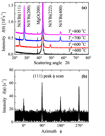
(a) Polar scans of films prepared at different temperatures. is the post-annealing temperature and is the substrate temperature. (b) NiYBi(111) azimuth scan.
The temperature dependence of the resistance of a 20 nm NiYBi film prepared at C is shown in Figure 2(a). The resistance decreases slowly with increasing temperature and suggests weak semiconducting behavior of the NiYBi films. This behavior was also observed in other half-Heusler semiconductors and is a typical characteristic of half-Heusler semiconductors as a result of heavy doping arising from composition deviationsCanfield et al. (1991); Oestreich et al. (2003). The low resistivity of the film results from the same reason rather than from the width of the band gap, which can be significantly enhanced by carrier neutralization in the film through doping Ouardi et al. (2010). The root-mean-square roughness of the film prepared at C is about 2.8 nm. The maximum value between peak and valley is approximately 29.8 nm. In order to check the influence of roughness on resistivity in NiYBi films, three samples with thicknesses of 20, 40, and 80 nm were deposited at C. Figure 2(b) shows the thickness dependence of the sheet resistance and resistivity. The fitted resistivity based on the sheet resistance (17.2 m) is the same as the average resistivity (17 m) measured from the three samples directly. This proves that the roughness hardly affects the resistance of the films.
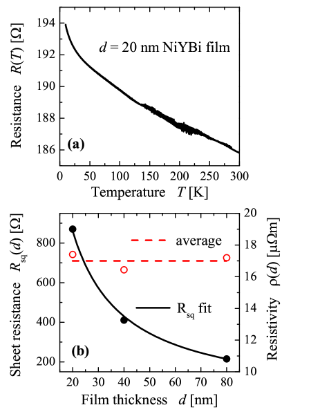
(a) Temperature-dependent resistance of a 20 nm NiYBi film. (b) Thickness dependence of sheet resistance (full symbols) and resistivity (open symbols).
The electronic structure of NiYBi was calculated using Wien2k Blaha et al. (2001), as described in detail in Reference Ouardi et al. (2010). The result is shown in Figure 3. The compound turns out to be a narrow gap semiconductor. The indirect gap between and has a width of meV. The optical gap at is also small, with a width of only 390 meV. The valence bands touching the Fermi energy have character at . The lower-lying states that cause a very high density of states at about -1.8 eV have character. The bottom of the upper part of the valence band is formed by states of character at . The states emerging from the Bi electrons are split off from the valence band and appear at about -11 eV.
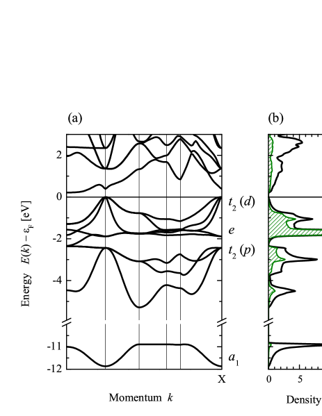
(a) shows the band structure and (b) the density of states. The density localized at the Ni atoms is marked by the shaded area. The labels assign the irreducible representations of the states at the point.
The HAXPES experiment was performed at BL47XU of Spring-8 (Japan). For details of the HAXPES experiment, see Ouardi et al. (2011); Kozina et al. (2011b, a). The valence band spectra of NiYBi are presented in Figure 4. The figure shows the valence band spectra excited by photons of energy about 8 keV with different polarizations and linear dichroism (). The high intensity at about -13 to -10 eV corresponds to excitation of the low-lying bands, as can be seen by comparison with the density of states (see Figure 3(b)). The intensity maximum centered at about -9 eV has no counterpart in the density of states of NiYBi. This arises from the MgO protective overlayer. Similar structures were previously also observed in the spectra from MgO-covered Co2MnSi Fecher et al. (2008). The upper part of the valence spectra above -6 eV exhibits the typical structure of NiYBi valence bands with three major maxima. In particular, the topmost of the three maxima exhibits a pronounced splitting. The spectra exhibit a clear cut-off at the Fermi energy. This is typical of -type materials, where the Fermi–Dirac distribution terminates the density of states slightly inside the valence band that is not fully occupied by electrons.
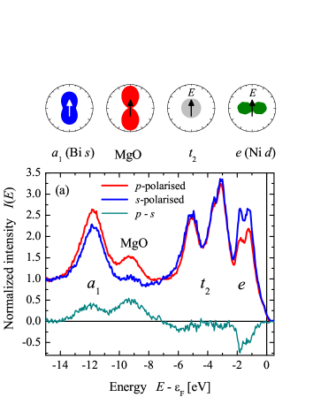
The figure shows the polarization-dependent valence band spectra , , and the difference . The spectra were obtained with a photon energy of about 8 keV. The emission characters of the different states are shown above the spectra in the upper part (note that the schematic intensities are not scaled by the cross-sections). Arrows indicate the direction of the electric field vector.
More differences in the intensities become obvious when the photon polarization is changed. In particular, for electrons, one expects lower intensities when using -polarized photons. This is because the angular asymmetry parameter becomes 2 for states in the spherical approximation, resulting in a vanishing intensity for -polarization. Similar to other Heusler compounds (compare with Reference Ouardi et al. (2011)), the intensity of the states does not vanish but is only reduced. The effect of the polarization is more pronounced at the MgO states (note the lower intensity but larger difference between the spectra in this energy region). This points to a parameter closer to 2 for these states. The relation between the linear dichroism (asymmetry ) and the angular asymmetry parameter is given by
| (1) |
for complete linear polarization of the photons. The linear dichroism asymmetries of the MgO and NiYBi states are (after subtraction of linear backgrounds) about 92% and 22%, resulting in angular asymmetry parameters of and , respectively. Assuming a slightly incomplete -polarization as a result of a small misalignment of the phase retarder, might come close to the expected value of 2, but even in that case, the parameter of the NiYBi state with cubic symmetry stays clearly below 1 and thus has a large deviation from spherically symmetric, atomic-type states with pure () character. The emission characteristics resulting from the different parameters are shown in the upper part of Figure 4.
Most parts of the valence band above -6 eV do not differ much when the polarization is changed, that is, the emission is rather spherically symmetric. The most distinct difference appears at -1.75 eV, where the intensity for - polarized light is higher than that of -polarized light. This is a result of the different characters of the and states. Here, this points to strong localization of the states at Ni, as is seen from the electronic structure in Figure 3.
In conclusion, -type semiconducting epitaxial NiYBi films were prepared directly on MgO(100) substrates. X-ray diffraction and HAXPES confirmed the good quality of the films in terms of crystalline and electronic structures, respectively. This material could therefore be a promising buffer layer or barrier in TIs, spintronic devices, and nanostructured thermoelectrics based on Heusler compounds, although the composition of the films may need to be further tuned for the specific requirements of these potential application.
Acknowledgements.
Financial support by the DFG-JST (project P 1.3-A in research unit FOR 1464 ASPIMATT) is gratefully acknowledged. HAXPES was performed at BL47XU of SPring-8 with approval of JASRI (Proposal No. 2011B1566).References
- Yang et al. (2008) J. Yang, H. Li, W. Zhang, L. Cheng, and J. Yang, Adv. Func. Mater. 18, 2880 (2008).
- Ouardi et al. (2010) S. Ouardi, G. H. Fecher, B. Balke, X. Kozina, G. Stryganyuk, C. Felser, S. Lowitzer, D. Ködderitzsch, H. Ebert, and E. Ikenaga, Phys. Rev. B 82, 085108 (2010).
- Chadov et al. (2010) S. Chadov, X. L. Qi, J. Kübler, G. H. Fecher, C. Felser, and S. C. Zhang, Nature Mat. 9, 541 (2010).
- Jaeger et al. (2011) T. Jaeger, C. Mix, M. Schwall, X. Kozina, J. Barth, B. Balke, M. Finsterbusch, Y. U. Idzerda, C. Felser, and G. Jakob, Thin Solid Films 520, 1010 (2011).
- Kozina et al. (2011a) X. Kozina, T. Jaeger, S. Ouardi, A. Gloskowskij, G. Stryganyuk, G. Jakob, T. Sugiyama, E. Ikenaga, G. H. Fecher, and C. Felser, Appl. Phys. Lett. 99, 221908 (2011a).
- Wang et al. (2010) S.-H. Wang, H.-M. Cheng, R.-J. Wu, and W.-H. Chao, Thin Solid Films 518, 5901 (2010).
- Fecher et al. (2008) G. H. Fecher, B. Balke, A. Gloskowskii, S. Ouardi, C. Felser, T. Ishikawa, M. Yamamoto, Y. Yamashita, H. Yoshikawa, S. Ueda, and K. Kobayashi, Appl. Phys. Lett. 92, 193513 (2008).
- Ouardi et al. (2011) S. Ouardi, G. H. Fecher, X. Kozina, G. Stryganyuk, B. Balke, C. Felser, E. Ikenaga, T. Sugiyama, N. Kawamura, M. Suzuki, and K. Kobayashi, Phys. Rev. Lett. 107, 036402 (2011).
- Canfield et al. (1991) P. C. Canfield, J. D. Thompson, W. P. Beyermann, A. Lacerda, M. F. Hundley, E. Peterson, Z. Fisk, and H. R. Ott, J. Appl. Phys. 70, 5800 (1991).
- Oestreich et al. (2003) J. Oestreich, U. Probst, F. Richardt, and E. Bucher, J. Phys.: Condens. Matter 15, 635 (2003).
- Blaha et al. (2001) P. Blaha, K. Schwarz, G. K. H. Madsen, D. Kvasnicka, and J. Luitz, WIEN2k, An Augmented Plane Wave + Local Orbitals Program for Calculating Crystal Properties (Karlheinz Schwarz, Techn. Universität Wien, Wien, Austria, 2001).
- Kozina et al. (2011b) X. Kozina, G. H. Fecher, G. Stryganyuk, S. Ouardi, B. Balke, C. Felser, G. Schönhense, E. Ikenaga, T. Sugiyama, N. Kawamura, M. Suzuki, T. Taira, T. Uemura, M. Yamamoto, H. Sukegawa, W. Wang, K. Inomata, and K. Kobayashi, Phys. Rev. B 84, 054449 (2011b).