Gating the charge state of a single molecule by local electric fields
Abstract
The electron acceptor molecule TCNQ is found in either of two distinct integer charge states when embedded into a monolayer of a charge transfer-complex on a gold surface. Scanning tunneling spectroscopy measurements identify these states through the presence/absence of a zero-bias Kondo resonance. Increasing the (tip-induced) electric field allows us to reversibly induce the oxidation/reduction of TCNQ species from their anionic or neutral ground state, respectively. We show that the different ground states arise from slight variations in the underlying surface potential, pictured here as the gate of a three-terminal device.
A goal of molecular electronics is to use single molecules as transistors AviramCPL74 ; ParkNature00 ; JoachimNature00 ; SongNature09 . To achieve this paradigm a high degree of charge localization in the device is required NitzanScience03 . Charge localization favors that a molecular device can only change its electron occupation in integer numbers, leading to discrete changes of its transconductance ParkNature02 ; LinagNature02 . However, a molecule contacted by metal electrodes generally shows non-integer charge states, in which the electron density is redistributed throughout the bond with the leads NitzanScience03 ; XuePRB03 . To achieve a large degree of charge localization, the interaction of the molecule with the metal leads has to be sufficiently weak. This is best achieved by introducing an ”effective tunneling barrier” to electronically decouple molecular states from the metal. Several STM studies on single molecules adsorbed on atomically clean and well-structured metal surfaces have shown that this is achievable using thin insulating layers (ionic or oxide thin films) separating the molecule from the surface WuPRL04 ; ReppScience04 ; ReppPRL05 ; PradhanNanolett05 ; FuPRL09 ; SwartNanoLett11 . A comparable level of decoupling has been observed when combining two different molecules in a monolayer directly adsorbed on a metal surface FrankePRL08 ; TorrentePRL08 . In this case, the proximity of the metal surface screens more efficiently charges localized at the molecule, leading to a reduction of Coulomb charging energy U and, hence, of the energy cost to change the electron occupation of the molecule TorrenteJPCM08 . Here, we find a similar degree of charge localization on the electron acceptor molecule tetracyanoquinodimethane (TCNQ) mixed with the electron donor tetramethyl-tetrathiafulvalene (TMTTF) in a stoichiometrically ordered monolayer. The methylation of the TTF backbone reduces the interaction of the molecular ad-layer with the metal substrate in comparison to the parent compound TTF-TCNQ TorrentePRL08 ; GonzLakPRL08 , while maintaining ground states with integer charge occupation.
A second requirement for molecules acting as electronic building blocks is the tunability of their charge state which would allow us to control the molecular transconductance Kouwenhoven01 . To change the charge state one needs an external handle (i.e. a potential) that shifts the alignment of molecular levels around the leads’ chemical potential. A successful approach consists in using the local electric field induced by the proximity of a metal STM tip to induce such shift WuPRL2004 ; PradhanPRL05 ; NazinPRL05 ; TeichmannPRL08 ; WiesendangerPRB2008 . In this case, the critical field for changing the charge state can be controlled by either the applied sample bias or the tip position.
In this Letter, we demonstrate the localization of charge and its manipulation by an electric field in individual electron-acceptor molecules embedded into a self-assembled monolayer on a metal surface. Tunneling transport measurements reveal the existence of two integer charge states that can be manipulated reversibly by means of a gating electric field, locally applied using the tip of a scanning tunneling microscope (STM). Our results suggest that this model molecular junction can be treated conceptually as a three-terminal transistor.
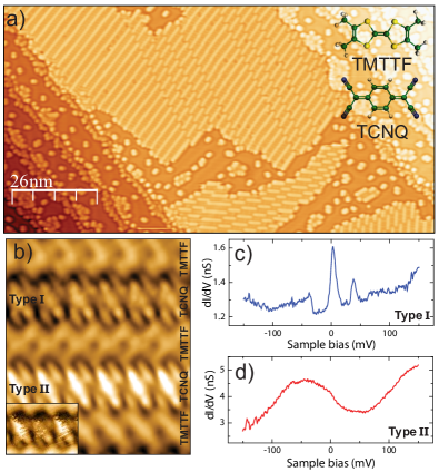
TMTTF-TCNQ monolayers are grown by sequential sublimation of the two compounds on an atomically clean Au(111) surface kept at room temperature and in ultra-high vacuum note1 . STM images, obtained at a base temperature of 4.8 K, show ordered molecular domains composed of electron-donor and -acceptor species alternating in molecular rows (Fig. 1a and 1b). The molecules interact among each other through their H (donor)-CN (acceptor) terminal groups, while keeping their backbone plane parallel to the metal surface. The TMTTF-TCNQ layer leaves the herringbone reconstruction intact and incorporates numerous dislocations in its structure (as shown in Fig. 1a). A crucial finding here is that TCNQ molecules show striking variations of their apparent height in the STM images at low bias; for example, molecules labeled Type I and Type II in Fig. 1b show a height difference of 20 pm, and some may even exhibit bistable behavior between the two heights during STM scanning [inset of Fig. 1b]. We will show next that the differences in apparent height are correlated with a different charge state of the TCNQ species.
To identify the electronic ground state of the two types of TCNQ molecules we use tunneling spectroscopy. Focusing first on the spectral region close to the Fermi level (E), the differential conductance plots on the darker TCNQ species (Type I) show a narrow (7 mV FWHM) zero-bias peak (ZBP), similar to that found on the parent TTF-TCNQ compound TorrentePRL08 . This ZBP is a manifestation of the spin Kondo effect and reveals that TCNQ molecules have a S=1/2 magnetic ground state. Such state is created by the occupation of the TCNQ LUMO with a single electron donated by its environment (here TMTTF and surface). The Kondo peak measured at the center of the molecule appears split in two side bands centered at 40 meV, corresponding to the excitation of an in-plane molecular vibration, which strongly couples with the TCNQ LUMO TorrentePRL08 . The spectra of the brighter molecules (Type II), in contrast, are rather flat without any indication of a Kondo resonance. They thus lie in a different, presumable neutral, electronic ground state.
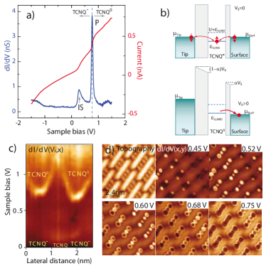
The charge state of the two types of molecules can be manipulated by increasing the electric field at the molecular junction. This is done by ramping the sample bias (Vs) in a wider bias range. Examples of the simultaneously recorded current and conductance spectra are shown in Figures 2a and 3a. On Type I molecules, the conductance plots show two types of features at positive bias (Fig. 2a): a step-like onset at 0.2 eV (IS), corresponding to a (molecular-induced) interface state note2 , and a sharp ”peak” (P). The position of peak P shifts gradually to lower values as the distance between tip and molecule is reduced (Fig. 2c), hence, as the electric field at the molecule is increased. This behavior is qualitatively interpreted by a double barrier tunneling junction (DBTJ).
In the DBTJ model (Fig. 2b) a small fraction of the applied bias potential drops between the molecule and the surface PradhanPRL05 ; NazinPRL05 ; DattaPRL97 . Correspondingly, the molecular levels shift by an amount Vs with respect to the surface chemical potential. In Type I molecules, a positive bias shifts the alignment of the singly occupied TCNQ- LUMO (i.e. the SOMO) to higher energy. Upon crossing the surface chemical potential, the SOMO is emptied, leaving the molecule in a neutral state. This sudden discharging causes a stepped increase of the tunneling current and, consequently, a sharp peak (P) in the differential conductance WuPRL2004 ; note7 .
The fraction increases as the tip approaches the molecule, and the double barrier junction becomes more symmetric. In full agreement with this model, constant current dI/dV maps in Fig. 2d show that the ”discharging” peak P is distributed around the TCNQ molecules with an elliptical contour, whose perimeter increases with the sample bias. These ellipses depict contours of constant electric field inducing the discharging NazinPRL05 ; PradhanPRL05 ; the region inside corresponds to the neutral specie, discharged by the proximity of the STM tip.
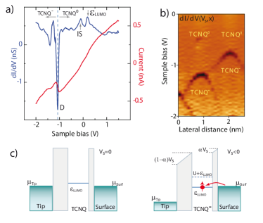
The spectra of brighter TCNQ molecules in Fig. 1b (Type II) show, in a similar energy scale, a quite different behavior (Fig. 3a). The most striking feature is a sharp dip (D) at negative bias, which, as for Type I species, shifts towards E for closer tip distances to the molecule (Fig. 3b). This property is thus a fingerprint of the opposite effect than peak P: the local charging (i.e. the reduction) of the TCNQ molecule induced by the field-driven downshift of their empty LUMO level below E (Fig. 3c) note7 .
The magnitude of the electric field which acts as a gate potential for molecular discharging/charging is controlled by adjusting the tip position with respect to the molecule. This control of the charge state thus resembles the situation in a three terminal device. The change in charge state of the molecule leads to a step in the tunneling current following the same trend for both type I and II molecules: charging a TCNQ molecule causes a partial blockade of the current (visualized as a step-wise decrease in the current spectra of Figs. 2a and 3a and the charging onset as the bias is scan from right to left), while discharging causes a substantial increase in the current. The lower tunneling transmission through negatively charged molecules is attributed to the interface dipole created by the anion and its image charge, resulting in an increase of the local work function note3 . This is also consistent with the lower apparent height of type I molecules in STM images at low bias (e.g. Fig. 1b).
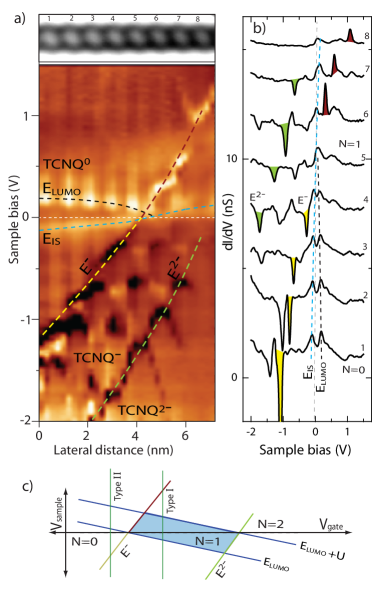
The existence of two ground states with different electron occupation is caused by subtle variations in the chemical equilibrium of TCNQ molecules with their environment. Inhomogeneities of the surface potential induce a modulation of the LUMO alignment with respect to the Fermi level note5 that eventually can lead to a change of the charge state along the molecular rows. Fig. 4a shows a dI/dVs(Vs,x) map collecting a series of spectra taken along eight TCNQ molecules embedded in an extended row. Accordingly, the spectral map shows a gradual shift of their features with the lateral position along the chain. The left most molecules are Type II (neutral) species (compare with individual dI/dVs plots extracted in Fig. 4b). Their spectra show a charging dip (marked by line in Fig. 4a) and the onset of the interface state (IS) at negative bias, as well as the unoccupied LUMO state (ELUMO line) slightly above E. All these features gradually shift towards E as we explore molecules towards the right. A cross-over to a different ground state occurs at the fifth molecule, where the three spectroscopic features cross through E. TCNQ molecules to the right of the fifth molecule lie in an anionic ground state. The line separating the neutral and charged state is now at positive bias, indicating the discharging peaks of the TCNQ anions. At the same time the LUMO resonance vanishes as it becomes singly occupied note9 and the interface state (IS line) becomes depopulated. This indicates that the interface state provides the charge required for the stabilization of the TCNQ anion.
Following the DBTJ model, the map in Fig. 4a allows us to obtain the bias fraction dropping at the molecule-metal interface. For Type II molecules, corresponds to the ratio , amounting to for the spectra in Fig. 4 note6 . This value is comparable with the one reported for molecules on alumina films NazinPRL05 . The small vacuum barrier underneath the TCNQ molecules behaves similar to thin insulating films with larger relative permeabilities
Below the line, a second conductance dip indicates the onset for doubly charging the TCNQ molecules ( line). The bias separation between the two charging lines ( 1.2 V), corrected by the factor , corresponds to a Coulomb charging energy U 180 meV. This value lies in the expected range for molecules on metal surfaces and is much smaller than the U in organic solids due to the charge screening effect of the underlying metal surface TorrenteJPCM08 .
The gradual shifts of the onset for charging/discharging with the position of the molecules within the chain resembles the transport characteristics of three-terminal quantum devices (as sketched in Fig. 4c), where the alignment of the quantum levels are tuned externally by a gate potential Kouwenhoven01 ; JarilloNature04 ; BrarNatphys11 . In these devices, the different charging states are represented as a set of Coulomb Diamonds appearing in spectral maps as a function of the applied gate and source-drain potential. In our experiments, the molecular charge state is shown to be tuned in two different ways: i) the finite voltage drop at the molecule-metal interface mimics a gating potential, which can be tuned by the tip-sample distance. ii) the local adsorption potential energy surface acts as a ”static” gate potential, tuning various charge states depending on the lateral position along molecular TCNQ rows (as in Fig. 4).
In summary, our results show that charge localization in molecular layers directly on a metal is possible at the level of reaching integer molecular charge states, which can be manipulated. We observed that TCNQ molecules may be found with two distinct oxidation states (anionic and neutral), depending on small variations of the underlying adsorption potential. These charge states are crucially affected by externally applied local electric fields, allowing tuning the molecular tunneling conductance by field effect.
We thank Jordi Fraxedas for driving us into this study, and Felix von Oppen and Tobias Umbach for stimulating discussions. This research has been supported by the DFG through grants FR2726, SPP1243 and Sfb658.
References
- (1) A. Aviram, M.A. Ratner, Chem. Phys. Lett. 29, 277 (1974).
- (2) C. Joachim, J.K. Gimzewski, A. Aviram, Nature 408, 541, (2000).
- (3) H. Park et al. Nature 407 57 (2000).
- (4) H. Song et al., Nature 462, 1039 (2009).
- (5) A. Nitzan and M.A. Ratner, Science 300, 1384 (2003).
- (6) J. Park et al., Nature 417, 722 (2002).
- (7) W. Liang, M. P. Shores, M. Bockrath, J. R. Long and H. Park, Nature 417, 7265 (2002).
- (8) Y. Xue, A. Ratner, Phys. Rev. B 68, 115406 (2003).
- (9) S.W. Wu et al., Phys. Rev. Lett. 93, 236802 (2004).
- (10) J. Repp et al. Phys. Rev. Lett. 94, 026803 (2005).
- (11) N.A. Pradhan et al. Nano Lett. 5, 55 (2005).
- (12) Y.-S. Fu et al., Phys. Rev. Lett. 103, 257202 (2009).
- (13) K.J. Franke et al., Phys. Rev. Lett. 100, 036807 (2008).
- (14) I. Fernández-Torrente, K.J. Franke, J.I. Pascual, Phys. Rev. Lett. 101, 217203 (2008).
- (15) I. Fernández-Torrente, K.J. Franke, J.I. Pascual, J. Phys.: Condens. Matt. 20, 184001 (2008).
- (16) N. Gonzalez-Lakunza et al., Phys. Rev. Lett. 100, 156805 (2008).
- (17) L.P. Kouwenhoven, D.G. Austing, S. Tarucha, Rep. Prog. Phys. 64, 701-736, (2001).
- (18) J. Repp et al., Science 305, 493 (2004).
- (19) I. Swart, T. Sonnleitner, J. Repp, Nano Lett. 11, 156805 (2011).
- (20) F. Marczinowski et al., Phys. Rev. B 77, 115318 (2008).
- (21) S. Wu et al., Phys. Rev. Lett. 93, 236802 (2004).
- (22) N.A. Pradhan et al., Phys. Rev. Lett. 94, 076801 (2005).
- (23) G.V. Nazin, X.H. Qiu, W. Ho, Phys. Rev. Lett. 95, 166103 (2005).
- (24) K. Teichmann et al., Phys. Rev. Lett. 101, 076103 (2008).
- (25) The Au(111) surface was cleaned by repetitive cycles of sputtering and annealing. Tungsten tips were prepared in situ by gently dipping them into the gold substrate until they show no tip-related spectroscopic feature. Sublimation temperatures of TMTTF and TCNQ are 90∘C and 140∘C, respectively.
- (26) This state resembles the interface band reported in ref. GonzLakPRL08 originated by the depopulation of the Au(111) surface state by charge donation into the acceptor molecule. This onset appears at negative sample bias when inspecting Type II molecules, reflecting the ”local” population of the interface band and, consequently an increase in the Density of State (DoS) at E underneath these species.
- (27) S. Datta et al., Phys. Rev. Lett. 79, 2530 (1997).
- (28) We note that these effects were not observed when using instead the parent specie TTF, but only after the incorporation of methyl terminations in the TTF backbone. This suggests that the methylation induces a larger separation of the TCNQ plane from the surface and, consequently, enhances the DBTJ behaviour.
- (29) It is remarkable that, upon charging Type II molecules at negative bias, the blockade induced by the formation of a local dipole is more important than the expected increase in tunneling transmission due to an additional resonance (the now singly occupied orbital) below E.
- (30) These variations are probably originated by the stress caused by the underlying Au(111) herring-bone reconstruction. Regions with many dislocation lines show only the anionic species and no reconstruction.
- (31) The two single particle peaks at SOMO and SOMO+U are expected to have less intensity in the spectra than the corresponding fully unoccupied (LUMO) resonance and, then, difficult to resolve Temirov .
- (32) R. Temirov, A. Lassise, F. B. Anders, and F. S. Tautz. Nanotechnology 19, 065401 (2008).
- (33) With increasing tip-sample distance this value decreases proportionally.
- (34) P. Jarillo-Herrero et al., Nature 429, 389 (2004).
- (35) V.W. Brar et al., Nature Physics 7, 43 (2011).
- (36) I. Horcas et al. Rev. Sci. Instrum. 78, 013705 (2007).