Nonequilibrium electron-vibration coupling and conductance fluctuations
in a C60-junction
Abstract
We investigate chemical bond formation and conductance in a molecular C60-junction under finite bias voltage using first-principles calculations based on density functional theory and nonequilibrium Green’s functions (DFT-NEGF). At the point of contact formation we identify a remarkably strong coupling between the C60-motion and the molecular electronic structure. This is only seen for positive sample bias, although the conductance itself is not strongly polarity dependent. The nonequilibrium effect is traced back a sudden shift in the position of the voltage drop with a small C60-displacement. Combined with a vibrational heating mechanism we construct a model from our results that explain the polarity-dependent two-level conductance fluctuations observed in recent scanning tunneling microscopy (STM) experiments [N. Néel et al., Nano Lett. 11, 3593 (2011)]. These findings highlight the significance of nonequilibrium effects in chemical bond formation/breaking and in electron-vibration coupling in molecular electronics.
pacs:
73.63.-b, 68.37.Ef, 61.48.-cI Introduction
The influence of an external bias voltage and electronic currents on the formation and breaking of chemical bonds is a topic of increasing importance with the continued down-scaling of electronic components. This is especially accentuated in the limit of single-molecule devices.Galperin et al. (2008)
A substantial current may flow through a single bond and its effect on the stability and impact on transport is crucial. The phenomenon of random two-level conductance fluctuations (TLF) is generally observed in a wide range of simple atomic and molecular contacts.Agraït et al. (1993); Donhauser et al. (2001); Wassel et al. (2003); Thijssen et al. (2006); Sperl et al. (2010) It is often possible to relate these to changes in the bonding configuration driven by the current. Clearly, controlled and reversible switching between well-defined conductance states is a useful function.Molen and Liljeroth (2010) Over the years many examples of atomicEigler et al. (1991); Stroscio and Celotta (2004); Sperl et al. (2010) and molecule-basedStipe et al. (1998); Choi et al. (2006); Henzl et al. (2006); Liljeroth et al. (2007); Danilov et al. (2008); Halbritter et al. (2008); Trouwborst et al. (2009); Kumagai et al. (2009); Mohn et al. (2010); Ohmann et al. (2010); Brumme et al. (2011); Huang et al. (2011); Kumagai et al. (2012) switches have been demonstrated. However, the understanding of how the nonequilibrium electronic structure impact chemical bonding and conformational changes still pose many open questions. First-principles calculations and comparisons with well-characterized, time-resolved experiments can shed light on these issues.
Nonequilibrium dynamics of C60-systems has been under intense studyPark et al. (2000); Danilov et al. (2008); Schulze et al. (2008); Néel et al. (2011). Here we focus on recently reported time-resolved measurements of single C60-contacts with a scanning tunneling microscope (STM),Néel et al. (2011) which showed that TLF occur in a narrow transition regime between tunneling and contact to C60. The advantage of STM is the possibility to identify the orientation of individual C60-moleculesLarsson et al. (2008); Néel et al. (2008) before and after controllable formation of the tip-molecule contact.Néel et al. (2007) Moreover, the role of detailed electrode bonding geometry Schull et al. (2009, 2011a) and contact point on the junction conductance has been clarified.Schull et al. (2011b)
More specifically, the experiment revealed the following interesting properties: (i) In the tunneling regime spectroscopy shows that transport is dominated by the lowest unoccupied molecular orbital (LUMO) (seen as a resonance centered at a positive sample voltage of V), while (ii) in contact the curve is close to linear in the voltage range V, suggesting a relatively symmetric coupling of the LUMO resonance to the two electrodes. Intriguingly, (iii) the TLF was only observed at positive sample voltage around contact formation. These findings were discussed in Ref. Néel et al., 2011 solely on the basis of spectra in the tunnel regime. Essentially, only the spectral properties of the molecular adsorbate in equilibrium with the substrate were considered. Here we present a different view on the experimental findings based on our demonstration of a remarkably strong bias-dependent electronic coupling to the center-of-mass (CM) motion of the C60 at the point when a bond is being formed between C60 and the apex atom of the STM tip. From first-principles calculations we obtain a detailed description of the C60-junction geometry as well as the molecular LUMO resonance near the Fermi level. This allows us to construct a model for the TLF, which provides an explanation for the experimental findings. Our results demonstrate that the full nonequilibrium electronic structure needs to be accounted for to understand the observed TLF.
Our paper is organized as follows. In Sec. II we describe the first-principles method and our setup of the C60-contact system. In Sec. III we then describe the results obtained without fitting parameters for the contact formation between STM-tip and C60 in equilibrium. Here we identify the formation of the chemical bond between the molecule and the tip apex atom. This is followed by our study of nonequilibrium effects and a discussion of the identified polarity-dependent strong coupling between the C60 CM motion and voltage drop (Sec. IV). From these first-principles calculations we extract in Sec. V parameters for a simple single-resonance model, most importantly the bias-dependent electron-vibration coupling to the CM motion. Together with a few additional parameters the model is used to calculate the TLF behavior, which can be compared to the experiment. Before concluding we discuss how the nonequilibrium forces modify the energy landscape for the CM-motion (Sec. VI).
II Method and setup
To study the contact formation and TLF we employ the SiestaSoler et al. (2002) density functional theory (DFT) method, and its extension to finite bias using nonequilibrium Green’s functions (DFT-NEGF) in the TranSiesta scheme.Brandbyge et al. (2002) The generalized gradient approximation (GGA-PBE) is applied for exchange and correlation (xc).Perdew et al. (1996)
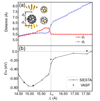
The C60 junction geometry is modelled as shown in the inset to Fig. 1. The periodic supercell used in the DFT calculations contains one C60 molecule supported on top of seven fixed Cu(111) layers (27 Cu atoms per layer) with a pyramid-shaped Cu tip mounted on the bottom layer. To accurately describe the Cu surface and the chemical bonding with C60, an optimized diffuse basis set was applied for Cu surface layers and the tip.Garcia-Gil et al. (2009) The counterpoise correctionBoys and Bernardi (1970) for the basis set superposition errors (BSSE) was applied to the total energy calculations, which was checked against complementary calculations with the Vasp Kresse and Furthmüller (1996) plane wave code as shown in Fig. 1(b).
The -point approximation was employed for Brillouin zone integrations in the electronic structure calculation, while the transmission function was sampled over k-points in the 2D Brillouin zone parallel to the electrode surfaces. The residual atomic forces were lower than 0.02 eV/Å for the atoms that were relaxed. The C60 CM force constant was calculated from DFT total energies corresponding to configurations where the C60 CM was rigidly displaced, up to Å from its equilibrium position.
III Contact formation
We first focus on the bond-formation point at zero bias, and consider the approach of the STM tip towards a 5:6 C60-bond, i.e., a bond between a pentagon and a hexagon. We note that the fluctuations were observed for this orientation in the experiments,Néel et al. (2011) and that no molecular rotations occur during contact formation in either the experimentsNéel et al. (2008) or in our structure optimizations.
We optimize the junction geometry by stepwise reducing the size of the DFT-supercell in the direction perpendicular to the surface, while relaxing the C60 and tip atoms. Fig. 1(a) shows the relaxed bond lengths and , between the C60 center-of-mass (CM) and the surface and the tip atoms, respectively, as a function of electrode separation . Around a characteristic separation Å, the distance decreases rapidly while increases dramatically as the cell shrinks. This signals the onset of a chemical bond formation between the STM tip and the C60 molecule. This tip-C60 attraction lowers the total energy of the system as witnessed by the binding energy curve in Fig. 1(b).
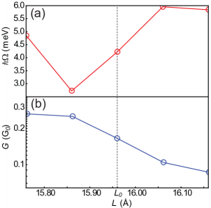
The corresponding vibrational energy associated with the C60 CM motion as well as the zero-bias conductance G (conductance quantum G) of the junction are shown in Fig. 2 in the transition regime between tunneling and contact for the DFT equilibrium geometries. At we find three eigenchannels contributing to the total transmission with the values . The first channel dominates the transmission, because the three-fold degeneracy of the C60 LUMO has been lifted.Hands et al. (2010); Heinrich et al. (2011) Thus, the C60 symmetry is broken in the contact configuration. One observes that the bond formation to the tip softens the C60-vibration [Fig. 2(a)] and increases the conductance by roughly a factor of 2.5 [Fig. 2(b)]. We note that the calculated conductance value of the order G0 agrees very well with the experimental conductance in the transition region between tunneling and contact where the TLF occur.Néel et al. (2011) Moreover, the calculated vibrational energies agree with a recent theoretical study of the C60 CM-motion on the Au(111) surface.Hamada et al. (2012)
According to our equilibrium DFT calculations we could not identify two well-defined stable configurations (for any fixed electrode separation) which could explain the existence of two different conductance states. Instead we observe a shallow energy landscape around the point of contact formation indicating that C60 is rather free to move between the electrodes (e.g., the softening of the C60 CM mode). We therefore speculate that a small barrier of the order of 10 meV, separating two distinct configurations, could be masked by limited numerical accuracy or by inherent approximations in the applied xc functional. In fact, recent theoretical studies of a somewhat simpler system consisting of graphene on Ni(111) have shown that various xc functionals can yield differences in the potential energies describing the carbon-metal distance much beyond the energies relevant for our system.Vanin et al. (2010); Wellendorff et al. (2012) The disregard of current-induced forces acting on the atoms could also play an important role in the energy landscape,Dzhioev and Kosov (2011) a point we return to at the end of this paper. Finally, we note that the actual experiments involve a complex reconstructed surface structure which we did not take into account. Because of these circumstances we shall therefore in our TLF-model (Sec. V) postulate the existence of two configurations in the contact region separated by a small barrier (on the order of DFT-accuracy), and instead focus our attention on the electron-CM vibration coupling and the resulting current-induced heating, which can explain the observed polarity-dependent TLF.
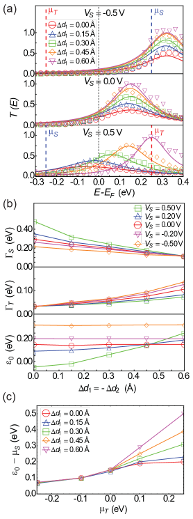
As the electrode separation is characteristic for the point of tip-C60 bond formation, we take this configuration as the starting point for an exploration of how the nonequilibrium electronic structure and electron transport depend on C60 motion. Fig. 3(a) shows the transmission spectra (with a prominent LUMO resonance) for several positions of C60 between the electrodes under three different applied sample voltages . In each situation the transmission function is approximately given by a Breit-Wigner functionDatta (1995); Novaes et al. (2011)
| (1) |
where
| (2) |
is the partial density of states of the LUMO resonance, positioned at , due to the coupling to the tip (sample) electrode (neglecting energy dependence in ). We take the equilibrium Fermi energy as the energy reference and define the tip and surface chemical potentials as and , respectively. The resonance parameters are readily fitted to the DFT-NEGF calculations as a function of C60-position and voltage, as shown in Fig. 3(b).
IV Voltage drop
Remarkably, the nonequilibrium electronic structure reveals a strong variation of with C60-position for positive sample voltages. This is a central finding of this work and below we shall show that it can explain the strong polarity dependence of the TLF seen in the experiments. In Fig. 3(c) we illustrate this by plotting the change in relative to , as a function of for the various C60-displacements. For the mainly follows , while for a small increase in and thus coupling to the tip, makes follow rather than , despite .
The voltage dependence of , or equivalently the voltage profile across the junction, can be understood roughly as a disposition of the system to maintain a constant electron charge in the resonance.Brandbyge et al. (1999) In order to illustrate this we consider a simple model calculation. Within the resonance model the LUMO charge is given by
| (3) |
If we assume constant LUMO charge independent of the applied bias, i.e., , we may determine the bias-dependent change in LUMO position, from Eq. (3). To mimic the change in C60-tip distance, , for fixed electrode distance, , we vary for fixed . In Fig. 4(a) it is seen how this simplified model reproduces the cross-over in the full DFT calculation [Fig. 3(c)] for positive sample voltage when the contact is formed. Thus the main voltage drop changes from being between tip and C60 for to being between surface and C60 when and the distance to the tip is decreased (). From Eq. (3) we can thus infer that in nonequilibrium there is a sensitive balance between coupling strengths () and electrode chemical potentials () that can displace the voltage drop from one interface to the other with a small relative change in coupling strengths.
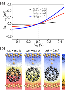
The voltage drop effect can also be seen directly in the actual voltage drop landscape (change in the one-electron potential with respect to equilibrium) shown in Fig. 4(b). The voltage drop is observed to shift from the C60-tip interface to the C60-substrate interface with a small C60-displacement, an effect not present for (not shown).
V Heating and fluctuations
We next explain how the strong variation of with C60-position for can be related to the strong polarity dependence of the TLF. We start by assuming that the main current-dependence comes from the excitation of C60 CM-motion, described by a harmonic potential with meV [cf. Fig. 2(a) at ]. Guided by the fact that the switching rates observed in the experiments (ms time scale) are very slow compared to CM oscillations, we propose that the switching involves a slow “bottle-neck” process, possibly involving tunneling along the reaction coordinate (RC), and that this process takes place when the excursion of the C60 () is beyond some critical distance from the equilibrium position. Inspired by the study of tunneling of a C60 molecule in the low-conductance regime Danilov et al. (2008) we express the switching rate as
| (4) |
i.e., as a product of the probability of C60 being at an excursion away from equilibrium and of a rate, , describing the slow process along the RC. The critical distance , or equivalently the energy barrier , controls how far the C60 needs to move in order to facilitate switching. The mean displacement , or equivalently the mean oscillator energy , are quantities which we can calculate within our TLF-model.
The excitation of the C60-CM motion by the current is determined from the electronic coupling to this motion. Using Fig. 3(b) we extract the electron-vibration coupling from the shift in resonance position with C60-displacement viaGao et al. (1997)
| (5) |
We evaluate the slope, , around Å, which is in the middle of the transition region [Fig. 3(b)], and note that the slope does not change significantly as we increase . The characteristic oscillator length is Å (C60 mass ), which is comparable to the size of the transition region in Fig. 2. The extracted electron-vibration coupling, , is shown in Fig. 5 as a function of sample voltage. A remarkably strong enhancement is evident for .
The excitation of the CM-motion, as seen in its mean energy , can be obtained from the bias-dependent rates of phonon emission, , and of electron-hole pair generation, . These rates can be determined within first order perturbation theory (Fermi’s Golden rule). Since is much smaller than all other electronic parameters, we may write
where . From these rates we can write a rate equation for the mean phonon occupation ,
| (8) |
where represents the vibrational relaxation due to anharmonic coupling to phonons in tip/substrate and is the Bose-Einstein (equilibrium) phonon occupation of the considered mode. The steady-state solution is simply
| (9) |
Following Refs. 48; 47 one can estimate a phonon damping to the substrate of C60-CM motion via the formula
| (10) |
where is the mass of a substrate atom, and meV a frequency characterizing the elastic response. This damping is likely to be exaggerated compared to the experimental situation since the C60 is adsorbed on a reconstructed surface with low-coordinated surface atoms and lower density of long wavelength phonons. This is a critical point for the explanation of the experimental result. We find that the best agreement is obtained for . In Fig. 6 we show how , , and varies with the sample voltage along with the effective temperature defined through a Bose-Einstein distribution . In all cases we see an enhancement for . If we use the mean occupation and effective temperature become a factor 100 smaller, but exhibit the same behavior as in Figs. 6(c)-(d). Finally we can calculate the oscillator energy as and thus the current-dependent rate from Eq. (4).
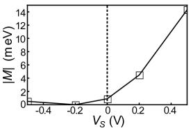
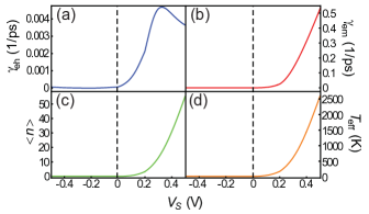
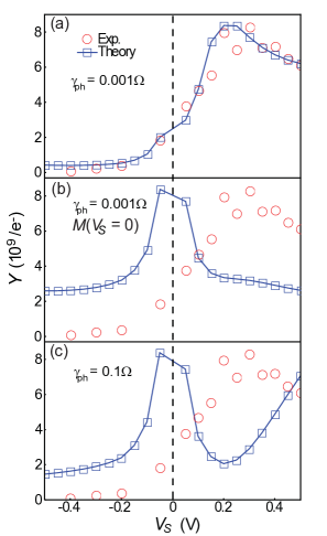
Fig. 7(a) shows how the calculated switching yield (blue squares), defined as the switching rate per tunneling electron, can reproduce the experimental data (red circles) if we use a barrier height of , a “tunnel-rate” ms-1, , and a background temperature of K as fitting parameters. The slightly elevated temperature, compared to the experiment performed at K, helps to smoothen the onset of the switching rate at small voltages. This can be justified by vibrational heating of other modes and their anharmonic coupling to the CM motion of the C60. The relatively slow is consistent with a tunneling process, and the small is consistent with the fact that we could not determine the barrier with our DFT calculations.
In Fig. 7(b) we show the calculated fluctuation rate in the case of constant zero-bias electron-vibration coupling where only the spectral energy-dependence of the molecule are considered, cf. the explanation presented in Ref. Néel et al., 2011 for the polarity dependence. However, it is clear that we are only able to reproduce the experimental results if we take the behaviour of the electron-vibration matrix element with bias into account. These findings suggests that (i) the strong polarity dependence of the switching is rooted in the nonequilibrium electron-vibration coupling in the transition region where the bond-formation between tip and C60 takes place, and (ii) that the reason for the observed saturation of the switching rate per electron is due to the steadily increasing electron-hole pair damping with bias, Eq. (V), so this becomes comparable with . This is an important point as illustrated in Fig. 7(c) where we show how the switching yield using the estimate grows for V (contrary to the experiment).
We note that the calculated current is roughly linear in voltage as in the experiments, and thus do not contribute significantly to the polarity dependence of the switching compared to the pronounced effect seen in Fig. 5 for the electron-vibration coupling . We further note that one theoretical studySergueev et al. (2005) has previously reported a nonlinear, polarity-independent for a smaller symmetric molecular junction and only at significantly higher voltages V.
VI Effect of current-induced force
In this section we estimate the change in the potential energy landscape in Fig. 1(b) when a nonequilibrium force is exerted on the C60–tip bond during contact formation. To calculate this additional bond force we consider the interaction between the C60 LUMO resonance and a wide band centered on the tip (see inset in Fig. 8). For this system we define the following two-site Hamiltonian
| (11) |
where we explicitly stress the dependence on bias and bond length . The interaction strength is calculated using , where is the wide band density of states on the tip, i.e., a constant which can be fitted to reproduce the transmission spectra in Fig. 3(a). The bond force is calculated using the general expressionTodorov et al. (2000)
where a factor of 2 is included to account for spin. The elements, and () of the density matrix D are determined from the spectral properties of the considered states,Brandbyge et al. (2003) which can be calculated from the fits in Fig. 3(b).
Since we only consider motion along a single coordinate the current-induced force is energy conserving, , enabling us to calculate the change in bond energy at a given bias,
| (13) |
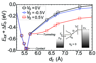
The integration limits are defined such that initially a contact is established, Å cf. the equilibrium curve in Fig. 8, and then we integrate along a path where the C60-tip contact is gradually separated. Addition of the energy term in Eq. (13) on top of the equilibrium total energy in Fig. 1(b) yields the bias-corrected curves shown in Fig. 8. Astoundingly, we see that only at positive a tiny barrier of the order a few meV may appear between two stable configurations corresponding to contact and tunneling cases, respectively. The origin of the significant lowering of the tunneling part of the binding energy curve for positive is related to the asymmetry in resonance position, which yields a large contribution from in Eq. (VI) only at positive . Finally, we note that the order of magnitude of the nonequilibrium barrier is in accordance with our assumption in the fluctuation calculation in Fig. 7.
VII Conclusions
In summary, we have presented the results of first-principles calculations which combined with a heating model and assuming a small energy barrier can explain the experimentally observed bias-dependent TLF observed in a C60 STM junction. Our main point is that the electron-vibration coupling can depend very strongly on the bias polarity. In this system we can trace this back to sensitivity of the nonequilibrium electronic structure/voltage drop with respect to the C60-motion just when the contact is being formed. The bias dependence of the electron-vibration coupling has so far not been considered in most calculations of inelastic electron transport and current-induced excitations. It remains to be answered to what extend this is important in general. In order to model the experimental switching we had to assume a small energy barrier for the C60-motion at the contact formation point. Although it is likely that the small barrier is masked by inaccuracy inherent in the DFT, the finite unit-cell employed, or numerical error, we showed that the nonequilibrium can induce significant changes in the potential energy surface. Our estimate of the current-induced force exerted on the C60-tip bond did indeed indicate an energy barrier for positive sample voltage.
In the presence of a significant current a number of different excitation mechanisms can become active. Recently, it has been discussed how current-induced forces can lead to “run-away” instabilities such as bond-rupture for highly conducting systems , and voltages in the range involved in the present experimentDundas et al. (2009); Lu et al. (2010). TLF experiments seems to be a promising way to probe these. The runaway effect requires the action of several vibration modes and we have limited our discussion here to a single mode. Our results demonstrate how the full nonequilibrium electronic structure can be of crucial importance for the formation/breaking of chemical bonds and electron-vibration coupling in the presence of current.
Acknowledgements.
We are grateful to Richard Berndt, Jörg Kröger, and Nicolás Néel for stimulating discussions and comments on an early version of our manuscript. We are also thankful to Hiromu Ueba for valuable suggestions. We also acknowledge computer resources from the DCSC.References
- Galperin et al. (2008) M. Galperin, M. A. Ratner, A. Nitzan, and A. Troisi, Science 319, 1056 (2008).
- Agraït et al. (1993) N. Agraït, J. Rodrigo, and S. Viera, Phys. Rev. B 47, 12345 (1993).
- Donhauser et al. (2001) Z. Donhauser, B. Mantooth, K. Kelly, L. Bumm, J. Monnell, J. Stapleton, D. Price, A. Rawlett, D. Allara, J. Tour, et al., Science 292, 2303 (2001).
- Wassel et al. (2003) R. Wassel, R. Fuierer, N. Kim, and C. Gorman, Nano Lett. 3, 1617 (2003).
- Thijssen et al. (2006) W. H. A. Thijssen, D. Djukic, A. F. Otte, R. H. Bremmer, and J. M. van Ruitenbeek, Phys. Rev. Lett. 97, 226806 (2006).
- Sperl et al. (2010) A. Sperl, J. Kröger, and R. Berndt, Phys. Rev. B 81, 035406 (2010).
- Molen and Liljeroth (2010) S. J. v. d. Molen and P. Liljeroth, J. Phys.: Condens. Matter 22, 133001 (2010).
- Eigler et al. (1991) D. M. Eigler, C. P. Lutz, and W. E. Rudge, Nature 352, 600 (1991).
- Stroscio and Celotta (2004) J. A. Stroscio and R. J. Celotta, Science 306, 242 (2004).
- Stipe et al. (1998) B. C. Stipe, M. A. Rezaei, and W. Ho, Phys. Rev. Lett. 81, 1263 (1998).
- Choi et al. (2006) B.-Y. Choi, S.-J. Kahng, S. Kim, H. Kim, H. W. Kim, Y. J. Song, J. Ihm, and Y. Kuk, Phys. Rev. Lett. 96, 156106 (2006).
- Henzl et al. (2006) J. Henzl, M. Mehlhorn, H. Gawronski, K.-H. Rieder, and K. Morgenstern, Angew. Chem. Int. Ed. 45, 603 (2006).
- Liljeroth et al. (2007) P. Liljeroth, J. Repp, and G. Meyer, Science 317, 1203 (2007).
- Danilov et al. (2008) A. V. Danilov, P. Hedegård, D. S. Golubev, T. Bjørnholm, and S. E. Kubatkin, Nano Lett. 8, 2393 (2008).
- Halbritter et al. (2008) A. Halbritter, P. Makk, S. Csonka, and G. Mihaly, Phys. Rev. B 77, 075402 (2008).
- Trouwborst et al. (2009) M. L. Trouwborst, E. H. Huisman, S. J. van der Molen, and B. J. van Wees, Phys. Rev. B 80, 081407 (2009).
- Kumagai et al. (2009) T. Kumagai, M. Kaizu, H. Okuyama, S. Hatta, T. Aruga, I. Hamada, and Y. Morikawa, Phys. Rev. B 79, 035423 (2009).
- Mohn et al. (2010) F. Mohn, J. Repp, L. Gross, G. Meyer, M. S. Dyer, and M. Persson, Phys. Rev. Lett. 105, 266102 (2010).
- Ohmann et al. (2010) R. Ohmann, L. Vitali, and K. Kern, Nano Lett. 10, 2995 (2010).
- Brumme et al. (2011) T. Brumme, O. A. Neucheva, C. Toher, R. Gutierrez, C. Weiss, R. Temirov, A. Greuling, M. Kaczmarski, M. Rohlfing, F. S. Tautz, et al., Phys. Rev. B 84, 115449 (2011).
- Huang et al. (2011) T. Huang, J. Zhao, M. Feng, A. A. Popov, S. Yang, L. Dunsch, and H. Petek, Nano Lett. 11, 5327 (2011).
- Kumagai et al. (2012) T. Kumagai, A. Shiotari, H. Okuyama, S. Hatta, T. Aruga, I. Hamada, T. Frederiksen, and H. Ueba, Nature Mater. 11, 167 (2012).
- Park et al. (2000) H. Park, J. Park, A. K. L. Lim, E. H. Anderson, A. P. Alivisatos, and P. L. McEuen, Nature 407, 57 (2000).
- Schulze et al. (2008) G. Schulze, K. J. Franke, A. Gagliardi, G. Romano, C. S. Lin, A. L. Rosa, T. A. Niehaus, T. Frauenheim, A. D. Carlo, A. Pecchia, et al., Phys. Rev. Lett. 100, 136801 (2008).
- Néel et al. (2011) N. Néel, J. Kröger, and R. Berndt, Nano Lett. 11, 3593 (2011).
- Larsson et al. (2008) J. A. Larsson, S. D. Elliott, J. C. Greer, J. Repp, G. Meyer, and R. Allenspach, Phys. Rev. B 77, 115434 (2008).
- Néel et al. (2008) N. Néel, J. Kröger, L. Limot, and R. Berndt, Nano Lett. 8, 1291 (2008).
- Néel et al. (2007) N. Néel, J. Kröger, L. Limot, T. Frederiksen, M. Brandbyge, and R. Berndt, Phys. Rev. Lett. 98, 065502 (2007).
- Schull et al. (2009) G. Schull, T. Frederiksen, M. Brandbyge, and R. Berndt, Phys. Rev. Lett. 103, 206803 (2009).
- Schull et al. (2011a) G. Schull, T. Frederiksen, A. Arnau, D. Sanchez-Portal, and R. Berndt, Nat. Nanotechnol. 6, 23 (2011a).
- Schull et al. (2011b) G. Schull, Y. J. Dappe, C. González, H. Bulou, and R. Berndt, Nano Lett. 11, 3142 (2011b).
- Soler et al. (2002) J. M. Soler, E. Artacho, J. D. Gale, A. Garcia, J. Junquera, P. Ordejon, and D. Sanchez-Portal, J. Phys.: Condens. Matter 14, 2745 (2002).
- Brandbyge et al. (2002) M. Brandbyge, J.-L. Mozos, P. Ordejon, J. Taylor, and K. Stokbro, Phys. Rev. B 65, 165401 (2002).
- Perdew et al. (1996) J. P. Perdew, K. Burke, and M. Ernzerhof, Phys. Rev. Lett. 77, 3865 (1996).
- Garcia-Gil et al. (2009) S. Garcia-Gil, A. Garcia, N. Lorente, and P. Ordejon, Phys. Rev. B 79, 075441 (2009).
- Boys and Bernardi (1970) S. F. Boys and F. Bernardi, Mol. Phys. 19, 553 (1970).
- Kresse and Furthmüller (1996) G. Kresse and J. Furthmüller, Phys. Rev. B 54, 11169 (1996).
- Hands et al. (2010) I. D. Hands, J. L. Dunn, and C. A. Bates, Phys. Rev. B 81, 205440 (2010).
- Heinrich et al. (2011) B. W. Heinrich, M. V. Rastei, D.-J. Choi, T. Frederiksen, and L. Limot, Phys. Rev. Lett. 107, 246801 (2011).
- Hamada et al. (2012) I. Hamada, A. Masaaki, and M. Tsukada, Phys. Rev. B 85, 121401(R) (2012).
- Vanin et al. (2010) M. Vanin, J. J. Mortensen, A. K. Kelkkanen, J. M. Garcia-Lastra, K. S.Thygesen, and K. W. Jacobsen, Phys. Rev. B 81, 081408(R) (2010).
- Wellendorff et al. (2012) J. Wellendorff, K. T. Lundgaard, A. Møgelhøj, V. Petzold, D. D. Landis, J. K. Nørskov, T. Bligaard, and K. W. Jacobsen, Phys. Rev. B 85, 235149 (2012).
- Dzhioev and Kosov (2011) A. A. Dzhioev and D. S. Kosov, J. Chem. Phys 135, 074701 (2011).
- Datta (1995) S. Datta, Electronic transport in mesoscopic systems (Cambridge University Press, 1995).
- Novaes et al. (2011) F. D. Novaes, M. Cobian, A. Garcia, P. Ordejon, H. Ueba, and N. Lorente, arXiv:1101.3714v1 (2011).
- Brandbyge et al. (1999) M. Brandbyge, N. Kobayashi, and M. Tsukada, Phys. Rev. B 60, 17064 (1999).
- Gao et al. (1997) S. Gao, M. Persson, and B. Lundqvist, Phys. Rev. B 55, 4825 (1997).
- Leiro and Persson (1989) J. Leiro and M. Persson, Surf. Science 207, 473 (1989).
- Sergueev et al. (2005) N. Sergueev, D. Roubtsov, and H. Guo, Phys. Rev. Lett. 95, 146803 (2005).
- Todorov et al. (2000) T. N. Todorov, J. Hoekstra, and A. P. Sutton, Philos. Mag. B 80, 421 (2000).
- Brandbyge et al. (2003) M. Brandbyge, K. Stokbro, J. Taylor, J.-L. Mozos, and P. Ordejon, Phys. Rev. B 67, 193104 (2003).
- Dundas et al. (2009) D. Dundas, E. J. McEniry, and T. N. Todorov, Nat. Nanotechnol. 4, 99 (2009).
- Lu et al. (2010) J.-T. Lu, M. Brandbyge, and P. Hedegard, Nano Lett. 10, 1657 (2010).