Electronic properties of graphene nanoribbons under gate electric fields
Abstract
Quantum-dot states in graphene nanoribbons (GNR) were calculated using density-functional theory, considering the effect of the electric field of gate electrodes. The field is parallel to the GNR plane and was generated by an inhomogeneous charge sheet placed atop the ribbon. Varying the electric field allowed to observe the development of the GNR states and the formation of localized, quantum-dot-like states in the band gap. The calculation has been performed for armchair GNRs and for armchair ribbons with a zigzag section. For the armchair GNR a static dielectric constant of could be determined.
pacs:
73.22.Pr, 85.35.Be, 71.15.Ap, 71.15.MbI Introduction
After their experimental realization, single and bilayer graphene sheets and nanoribbons have attracted intensive attention due to their peculiar properties, which make graphene and its derivatives one of the most prominent material classes for future nanoelectronics.Geim and Novoselov (2007); Castro Neto et al. (2009); Geim (2009) The vast range of possible applications is due to the high carrier mobility,Novoselov et al. (2005); Zhang et al. (2005); Avouris et al. (2007); Das Sarma et al. (2011) and remarkably long spin lifetimes and phase coherence lengths, which are particularly valuable for quantum information processing.Trauzettel et al. (2007) The peculiar electronic structure of gapless semiconductor graphene prevents electrostatic confinement due to Klein tunneling and gives rise to unique transport properties.Katsnelson et al. (2006) Experimentally, graphene-based tunable nanodevices can be realized, as shown, e.g., for graphene nanoribbons,Chen et al. (2007); Han et al. (2007); Li et al. (2008) interference devices,Miao et al. (2007); Russo et al. (2008) and graphene quantum dots.Stampfer et al. (2008a); Ponomarenko et al. (2008) Graphene nanoribbons (GNRs) play a particularly important role since they are often used in field-effect transistors (FET) setups where the current flow is regulated by a gate electric field. Additionally, gated nanoribbons can also be used to create quantum dots. Hereby, the spin qubits in quantum dots are a promising candidate for quantum information processing,Loss and DiVincenzo (1998) for which graphene is better suited than III–IV semiconductors due to its reduced hyperfine coupling and spin-orbit interaction.Trauzettel et al. (2007); Kane and Mele (2005); Min et al. (2006); Huertas-Hernando et al. (2006); Stampfer et al. (2008b); Liu et al. (2009) For nanoelectronics applications, the preferred width of a GNR is in the range of 1–3 nm as for wider ribbons the band gap diminishes.Son et al. (2006); Fiori and Iannaccone (2007)
For a proper theoretical description of GNR FET and GNR-based quantum dots, both the effect of an external electric field and the precise electronic structures of the ribbons have to be considered. In ribbons of small width the details of the termination and exact structure of the edges play an important role for ribbon’s electronic structure due to the quantum confinement effects, which have to be properly taken into account. The two most common types of edge termination of the ribbons lead to very different electronic structures in the vicinity of the Fermi energy: while armchair ribbons are insulating with a band gap of up to approximately 2.5 eV, zigzag ribbons exhibit metallic edge states.Fujita et al. (1996); Wang et al. (2007) For the former, the band gap decreases with increasing width of the ribbon and oscillates in magnitude with a periodicity of three as more rows of carbon atoms are added.Son et al. (2006) Experimentally, armchair ribbons with the width of 1 nm with well-defined edgesCai et al. (2010) and FET with widths down to 2 nm have been realized.Wang et al. (2008) On the other hand, ribbons with the width of around 50 nm have been used to create quantum dots.Ponomarenko et al. (2008); Güttinger et al. (2010)
The sensitivity of the electronic properties of narrow GNRs to an external electric field and to the details of the structure, as well as the mechanism for the formation of the quantum dot states, calls for a description and analysis within the highly accurate density-functional theory techniques (DFT). In this work, we study the properties of narrow GNRs in an electric field, generated by finite gates, by employing a new scheme specifically designed for this purpose and realized within the full-potential linearized augmented plane-wave (FLAPW) method. In contrast to common approaches, the latter scheme allows to consider any given distribution of charge in the gates, thus enabling the versatility necessary for studies of complex nanostructured devices from first principles. Here, we describe the details of this approach as implemented within the FLAPW method,Krakauer et al. (1979) and study the development of the electronic structure and screening properties of narrow GNRs as the strength of the electric field is varied. We focus particularly on the emergence of the quantum-dot like states, localized under the gates, and analyze their spatial distribution and symmetry properties.
II Inclusion of the electric field
In a realistic device the electronic properties of the graphene nanoribbon will be modified by gate electrodes. While more complex interactions between the gates and the graphene nanoribbon exist, the most prominent effect of the gates is the electric field they generate. These electric-field effects can be included in a calculation based on DFT,Hohenberg and Kohn (1964); Kohn and Sham (1965); Fiolhais et al. (2003) and in the past several different implementations of external fields in DFT codes have been reported.Bengtsson (1999); Neugebauer and Scheffler (1993); Meyer and Vanderbilt (2001); [][(inGerman).]phd:Erschbaumer; Erschbaumer et al. (1990); Heinze et al. (1999); Weinert et al. (2009) However, in contrast to most of these approaches, which model a situation in which the electric field is applied normally to a surface, the key effect of the gates we study is the field and potential distribution in the plane of the graphene ribbon.
II.1 Computational scheme
We use the film FLAPW methodKrakauer et al. (1979) as implemented in the fleur codeFLEUR for our calculations. Two slightly different schemes to include the electric fields of the gates have been tested in which the effect of the gates is modeled by: (i) a charged sheet far in the vacuum in which the charge varies parallel to the GNR or (ii) a plane in the vacuum at which a varying boundary condition to the Coulomb potential is applied. While the second approach is closer to the picture of a metallic gate applying an electric field, the generation of the potential from a charge distribution is performed in all existing DFT codes and, hence, the first approach is easy to implement. We discuss all details of the implementation of the gate electric field in the appendix.
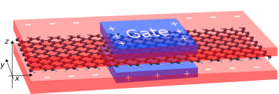
For modeling the effect of a gate electrode on a GNR we have chosen a free-standing 13-carbon-atom-wide graphene nanoribbon of armchair type [see Fig. 1(a)]. The dangling bonds are passivated using hydrogen leading to a ribbon which is about 5.1 nm long and 1.7 nm wide, consisting of 312 carbon and 48 hydrogen atoms. The setup is periodically repeated in -direction to form an infinite ribbon. As our code requires a two-dimensional periodicity, we also have to repeat the ribbon in direction. A supercell approach with a separation of 5 Å between adjacent cells is used to simulate a single isolated GNR. The center of the GNR is sandwiched between positively charged top and back gates whose charge is compensated by negatively charged top and back gates such that both the GNR and the two charge sheets remain as a whole charge neutral. The positively charged gate has a size of Å2 and the distance between the GNR plane and the charge sheets is 7 Å. For simplicity, we used a homogeneous surface-charge-density distribution on the gates [method (i)]. However, for the dimensions of this system, the potential at the position of the plane of the GNR is qualitatively the same for a gate with constant potential – the potential only differs strongly close to the gate (not shown). The calculations were performed with the Perdew-Burke-Ernzerhof (PBE) exchange-correlation functional.Perdew et al. (1996)
II.2 Screening of the electrical field
The height dependence ( dependence) of the electric field is shown in Fig. 1(b), cutting vertically through the GNR (with being at the middle of the ribbon). In the plane of the ribbon (), the field is fully in plane and parallel to the direction. Above the plane (), an out-of-plane component exists, which grows towards the center ( Å) and the left/right side ( and Å). At exactly those points, the field is perpendicular to the GNR plane and the field strength is low, while for the points in between the field is nearly in-plane and stronger. Thus, the potential should cause a charge accumulation under the gate.
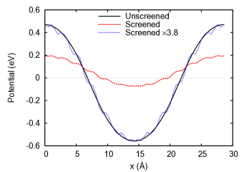
Figure 2(a) shows the gate potential along the center of the ribbon for a gate charge of nm2. These curves have been obtained by subtracting the total potential without an applied field from the potential with applied gate field canceling the potential from the mostly inert ion cores. The (in-plane) applied electric field at the position of the ribbon is given by the slope of the solid black curve and has a maximal value of 0.056 eV/Å. The initial potential due to the applied electric field (black solid curve) gets reduced (red dashed curve) due to the screening by the electrons in the ribbon. This screening effect is determined by evaluating the potential of the self-consistent calculation. From the reduction – the blue dotted curve has been obtained by multiplying the red dashed curve by 3.8 to match the black solid curve – a static () dielectric constant can be deduced for the center of the ribbon. As the calculation has periodic boundary conditions (in -direction) this static dielectric constant corresponds to a wavevector of . The value of agrees with the GW results of Ref. van Schilfgaarde and Katsnelson, 2011. One should note, that the static dielectric constant has been evaluated in the linear response limit of a small electric field, for stronger fields and especially close to the crossover of states [cf. Fig. 4(b)], different values are obtained.Burnus et al.
The dependence of the screening on the distance from the GNR plane is shown in Fig. 2(b); reduces only slightly from 3.8 to 3.4 over 1 Å. This relatively constant screening corresponds to presence of change density due to the orbitals, which is still significant at these distances. For larger distances to the GNR decreases exponentially, approaching the vacuum value of 1.
(a)
(b)

(a)
 (b)
(b)

(a)
 (b)
(b)
 (c)
(c)
 (d)
(d)
 (e)
(e)
 (f)
(f)
 (g)
(g)
 (h)
(h)
III Results
III.1 Straight armchair ribbon
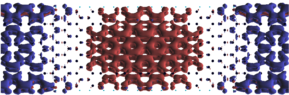
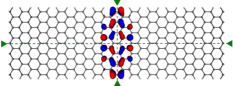
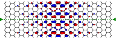
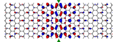
In this section, we focus on the formation of quantum dot states in an armchair GNR with a width of 13 carbon atoms by applying an electric field as outlined in the previous section. The edges of the ribbon are hydrogen-terminated and it is placed between the electrodes as visualized in Fig. 1(a). If one compares the total electron density of this structure without field and with a field of 0.67 V/Å (this corresponds to a charge of /nm2 on the gates), the charge accumulation and depletion can be visualized by a density-difference plot as shown in Fig. 3. Predominately charge of the orbitals is localized under the positively charged gate forming a “quantum dot” of about 20 Å diameter.
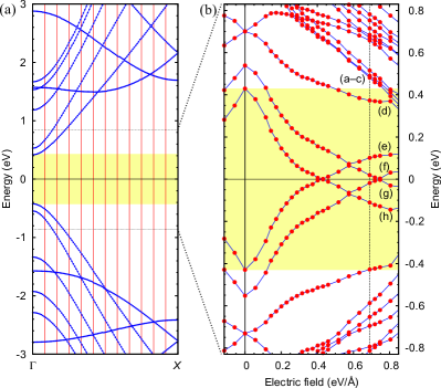
To investigate the effect of the electric field on the electronic structure of the GNR, we first consider in Fig. 4(a) the bandstructure of the ribbon without field. The bandgap is about 0.9 eV and bounded by valence and conduction band states at the point. Introducing an additional periodicity in -direction by the field leads to a backfolding of the bandstructure along –. If the field is modulated with a periodicity of 51 Å (12 unit cells in -direction), the backfolding occurs at the red lines shown in Fig. 4(a). The Brillouin zone extends then from to . In the following we focus on the states at the point, since they form the valence and conduction band edge.
Switching on the electric field leads to a splitting or a shift of the eigenenergies as shown in Fig. 4(b): The two-fold degeneracy of the states at eV and eV, which results from the backfolding of the Brillouin zone, is lifted and the bands split almost symmetrically, both for negative and positive fields. The slight asymmetry between positive and negative electric field is introduced by the shape of the gate electrode as shown in Fig. 1(a). If there were just a one-dimensionally modulated field acting on the GNR, this asymmetry would vanish. The splitting can then be understood from the consideration of a system with just two eigenstates with energies and , perturbed by a periodic potential with Fourier coefficients . At the backfolding of the bandstructure, the states split according to . As the states are degenerate, the splitting is linear in . In case of interacting states that are non-degenerate, the evolution of these states starts parabolic at small fields and evolves into a more linear behavior at stronger fields ().
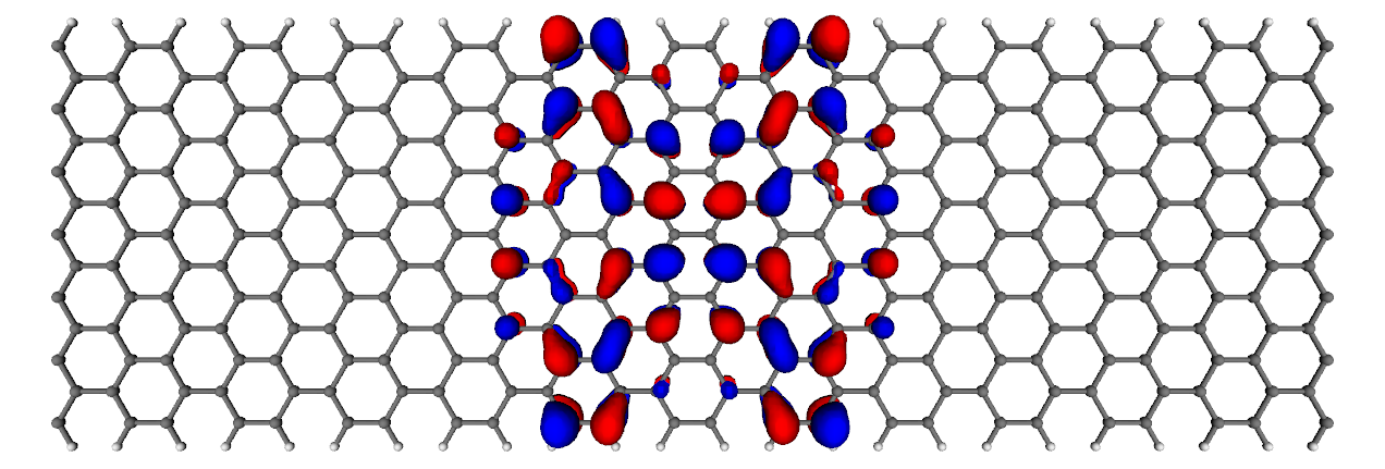
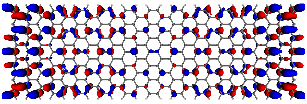
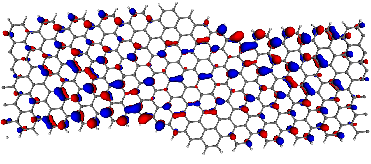
With increasing field strength the uppermost valence band states move up in energy, towards the Fermi level, while the lowest conduction band states move down by a similar amount. Their interaction causes again a deviation from the linear behavior and at a field strength corresponding to 0.4 V/Å the first crossover of states occurs, i.e. a valence band state becomes unoccupied while a conduction band state is populated. In order to get a better understanding of this scenario, we display the single-particle states in this energy region in Fig. 5 for a field of 0.67 eV/Å [vertical line in Fig. 4(b)]. The first crossover occurs for states shown in Fig. 5(e) and (h), i.e. with state (h) the first quantum dot state gets localized under the gate electrode. State (e) has more density outside the positively gated region; it raises in energy with increasing field and gets unoccupied.
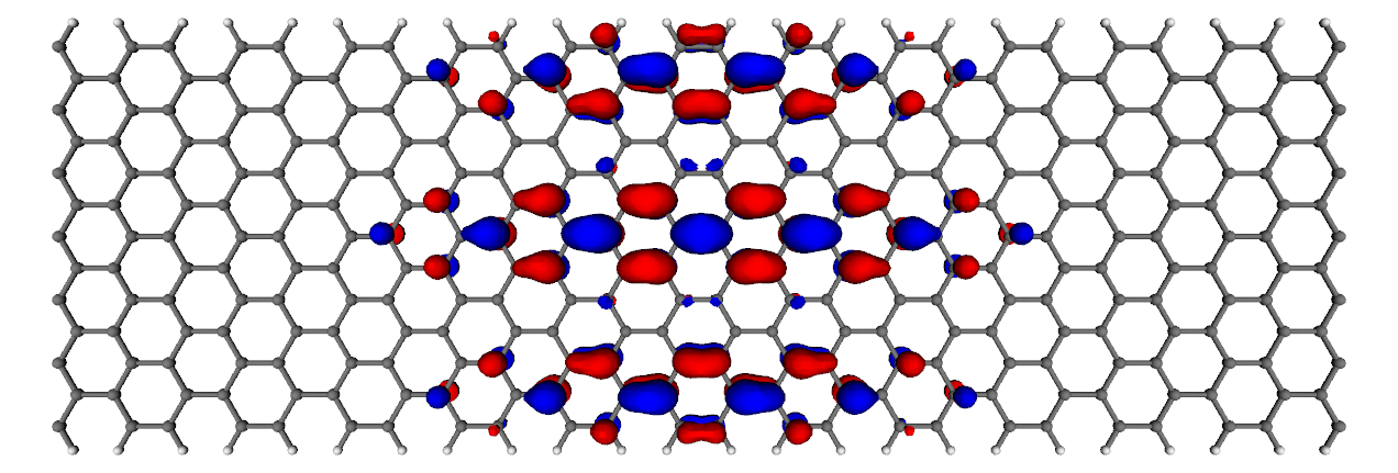
At stronger fields (0.72 eV/Å) the state Fig. 5(f) gets occupied, which can be regarded as the second quantum dot state. As for atoms, one expects also for quantum dots states an increasing number of nodal planes for higher states with higher energy, which is indeed what one observes: The color of the isosurfaces in Fig. 5 denotes the sign of the wavefunction, which allows to locate the nodal planes. The first quantum-dot state (h) has at the center one vertical nodal plane (dashed green line) and is not nodeless as one might have expected. For the next localized state (f) one sees in the charge density a horizontal nodal plane, while the state (c) has two: a horizontal and a vertical nodal plane. The state (b) seems to have two horizontal and the state (a) one horizontal and two vertical nodal planes.
We have thus shown how under a gate electric field, localized states appear in the band gap; those show a nodal structure as one expects for a quantum dot. The states still show the structure of the underlying lattice and are predominately formed by states as one can see in the charge density.
III.2 Z-shaped ribbon
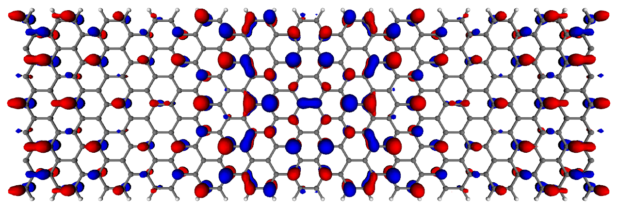
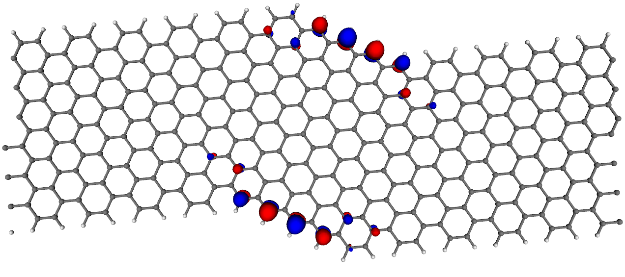
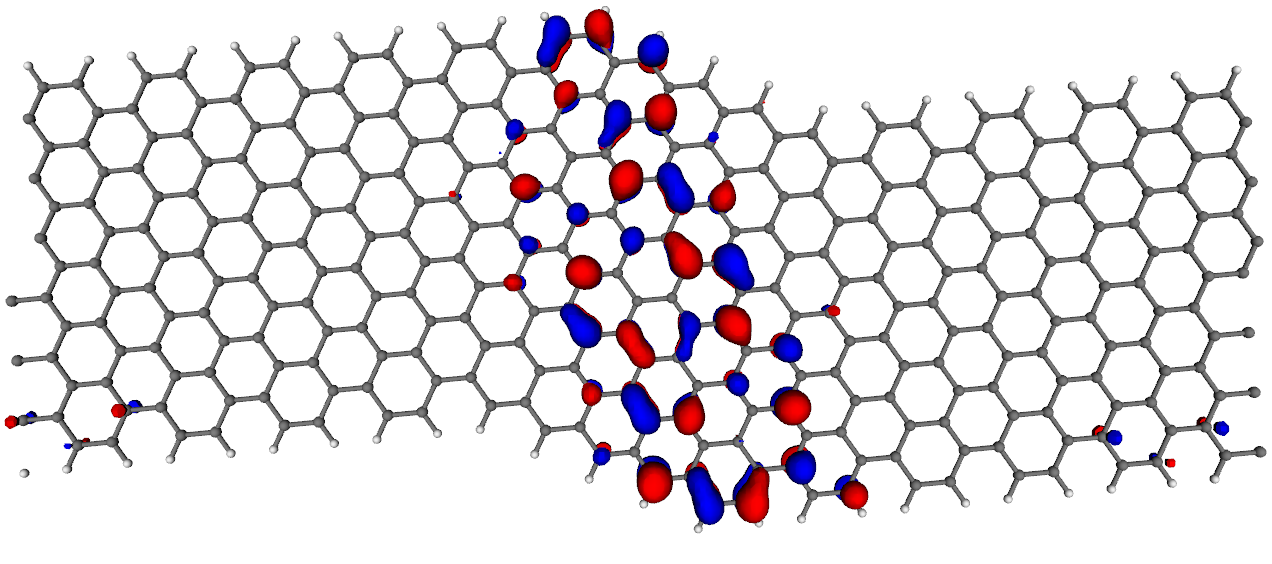
Besides armchair nanoribbons, also zigzag ribbons exist, which are known for their (conducting) edge states.Fujita et al. (1996); Nakada et al. (1996); Wang et al. (2007) Those are located just above and below the Fermi energy. The combination of both types of edge states could be useful for future nanodevices; but missing atoms or sections with different edge terminations might also occur involuntarily during the preparation of nanoribbons. We have thus simulated an armchair ribbon of width 13 (as above) but with a zigzag section in the middle.
For the calculation, a supercell with length of 51.3 Å and width of 25.8 Å has been used; the positive gate charge has been placed at the center over and below the zigzag region ( Å2). Figure 6(a) shows (for zero field) the existence of an edge state in the zigzag section; the highest occupied (shown) and the lowest unoccupied state have the same density but locally different phases. If one now turns on an electric field, the edge states gain density in the middle of the ribbon. Additionally, states with more density at the outside raise in energy, while more localized states get more localized and become lower in energy. This is exemplified in Fig. 6 for an electric field of 1 eV/Å (maximal potential gradient before screening; gate charge is /nm2): (b) shows a high lying state at zero field (0.87 eV above the Fermi energy), which moves down in energy to the Fermi energy in the electric field; at the same time its density becomes more localized at the zigzag region, i.e. under the gate.
(a)
(b)
(c)
IV Conclusion
A scheme to include arbitrary electrical fields has been introduced and its implementation for the film FLAPW method outlined. The scheme allows for Neumann and Dirichlet boundary conditions and for differently shaped gate electrodes. Future use could encompass the calculation of the effects of an electrical field on adatom on films and a wide range other electric-field related phenomena.
The gate electric field was then applied to an armchair graphene nanoribbon; the mostly in-plane field caused a charge accumulation under the gate. For small fields, the linear response of the electrons in the ribbon to the electric field allowed to determine a static dielectric constant of . The field also drove states into the zero-field gap; as has been shown, the previously unoccupied states entering the gap region are localized under the gate. Those states, mostly formed by orbitals, show the structure of the underlying lattice. However, they also feature a nodal structure as one would expected for quantum dots. The states have been obtained from an all-electron density-functional theory calculation, which makes a comparison to less precise techniques such as tight binding interesting; those techniques have the advantage that much larger systems can be treated. Additionally, the influence of the electric field on GNR consisting of zigzag with metallic edge states and semiconducting armchair sections has been shown, where the electric field moves states towards the Fermi energy, which are localized under the gate.
Acknowledgements.
The calculations were performed on the Juropa supercomputer at the Forschungszentrum Jülich, Germany. The work was supported by Deutsche Forschungsgemeinschaft through Research Unit 912 “Coherence and Relaxation Properties of Electron Spins”. Y. M. acknowledges funding under the HGF-YIG programme VH-NG-513.Appendix A Electric field in FLAPW
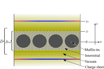
For periodic systems, the full-potential linearized augmented plane wave (FLAPW) basis, used for the calculations presented above, gives an accurate, all-electron description.Marcus (1967); Koelling and Arbman (1975); Andersen (1975); Krakauer et al. (1979); Wimmer et al. (1981); Weinert et al. (1982); Singh and Nordstrom (2006) Besides the more common FLAPW basis with three-dimensional periodicity, a film version of FLAPW exists. It has only two-dimensional periodicity and semi-infinite vacua in the third direction (chosen to be ).Krakauer et al. (1979); Wimmer et al. (1981); Weinert et al. (1982); [][andreferencestherein.]inbook:Bluegel2006; Kurz (2000) Hereby, the space is separated into three regions: the muffin-tin spheres around each atom, the interstitial region between the spheres and a vacuum region in which the density decays exponentially to zero; see Fig. 7. The basis set used for expansion of the wavefunction consists of the functions of the following form:
| (1) |
where is the reciprocal lattice vector, the are radial functions with as their energy derivatives, are spherical harmonics, , and and are coefficients chosen such that the basis function is continuously differentiable across the interstitial–vacuum and interstitial–muffin-tin boundary. The denotes the in-plane (–) and the out-of-plane () component. While the interstitial extends to , the perpendicular wavevectors are defined with regard to , i.e. , to allow for more variational freedom.
A.1 Neumann boundary conditions
The idea is to obtain the potential by integrating the surface charge density from infinity, i.e.
| (2) |
with , where is the charge density. The complication in evaluating the equation (2) arises from the use of different bases in the different regions. The electric field could be included in the calculation via its associated potential as an additional term to the external potential ; however, in the presented scheme it enters as charge density . Their relation is given by , where is the electric constant (for cgs replace by ).
For the vacuum region, the charge and the potential can be expanded in a Fourier series,[][(inGerman).]phd:Erschbaumer; Erschbaumer et al. (1990); Weinert et al. (2009)
| (3) |
thus, the Laplace operator of the Poisson equation separates into a and term,
| (4) |
which leads to two equations. For (uniform field in the vacuum), Eq. (4) can be solved by integration. Using the boundary condition that the potential smoothly vanishes at infinity, and , the potential in the vacuum is given by
| (5) | |||||
For the nonuniform part, , the Green function
| (6) |
can be used to give a particular solution for the potential,
| (7) |
which fulfills the boundary condition that the potential vanishes for smoothly at infinity.
If the system has no mirror symmetry, e.g. because the field on the top is different from the one at the bottom, the charge density can be written asErschbaumer (1988); Weinert
| (8) | |||||
| (9) |
where denotes the average pseudo charge density of the interstitial, i.e.
| (10) | |||||
with and Bessel function . To obtain the potential, one sums up the surface charge densities starting from minus infinity; the electric field is included as surface charge density . For the vacuum region, the component of the potential is given by
| (11) | |||||
| (12) |
where is the potential at and is a phase due to the dipole moment, which is only present if the system has neither mirror nor inversion symmetry. The potential is given by
| (13) | |||||
where .
For the component the solution is given by Eq. (7); for the FLAPW basis, the integration has to be split into two vacua and the film region; for a given the integral in the vacuum can be further split into and , which has been done to obtain the functions and below; the vacuum potential is then given by
| (14) | |||||
with
| (15) | |||||
| (16) |
where and is the (inhomogeneous) surface charge density of, respectively, the top and bottom charge sheet.
A.2 Dirichlet boundary conditions
Contrary to the Neumann boundary condition used above, which defines the boundary via a surface charge density, the Dirichlet boundary condition has a fixed potential at the boundaries, which matches metallic plates held a certain voltage. The Dirichlet boundary conditions not only imply a different single-particle potential but due to the density-dependent image charges the effective Coulomb interaction between electrons is modified.Hallam et al. (1996); Indlekofer et al. (2005) The effect of the latter is not included in the described scheme and would require a modified functional.
For the constant-potential boundary condition, the part, solved by integrating Eq. (4), is given by
| (17) | |||||
with . The lower boundary is set to , the location of the metallic plate with the associated potential . For the other plate at , the potential is given by
| (18) |
thus,
| (19) |
which can be used in a similar way to the Neumann solution described above.
To solve the Poisson equation for , we start with the solution of the homogeneous problem , which is given by
| (20) |
The coefficients and have to be chosen such that the boundary condition and are fulfilled; one obtains
| (21) |
which vanishes at the boundary ; for it simplifies to Eq. (6). Using this Green’s function, the particular solution is given by
| (23) |
Combining the regular solution of the homogeneous system with the particular solution gives
| (24) | |||||
with the and as defined above.
References
- Geim and Novoselov (2007) A. K. Geim and K. S. Novoselov, “The rise of graphene,” Nature Mater. 6, 183 (2007), arXiv:cond-mat/0702595 [cond-mat.mtrl-sci] .
- Castro Neto et al. (2009) A. H. Castro Neto, F. Guinea, N. M. R. Peres, K. S. Novoselov, and A. K. Geim, “The electronic properties of graphene,” Rev. Mod. Phys. 81, 109 (2009), arXiv:0709.1163 [cond-mat.other] .
- Geim (2009) A. K. Geim, “Graphene: Status and prospects,” Science 324, 1530 (2009), arXiv:0906.3799 [cond-mat.mes-hall] .
- Novoselov et al. (2005) K. S. Novoselov, A. K. Geim, S. V. Morozov, D. Jiang, M. I. Katsnelson, I. V. Grigorieva, S. V. Dubonos, and A. A. Firsov, “Two-dimensional gas of massless Dirac fermions in graphene,” Nature (London) 438, 197 (2005), arXiv:cond-mat.mes-hall [cond-mat/0509330] .
- Zhang et al. (2005) Y. Zhang, Y.-W. Tan, H. L. Stormer, and P. Kim, “Experimental observation of the quantum Hall effect and Berry’s phase in graphene,” Nature (London) 438, 201 (2005), arXiv:cond-mat/0509355 [cond-mat.mes-hall] .
- Avouris et al. (2007) P. Avouris, Z. Chen, and V. Perebeinos, “Carbon-based electronics,” Nat. Nanotechnol. 2, 605 (2007).
- Das Sarma et al. (2011) S. Das Sarma, S. Adam, E. H. Hwang, and E. Rossi, “Electronic transport in two-dimensional graphene,” Rev. Mod. Phys. 83, 407 (2011), arXiv:1003.4731 [cond-mat.mes-hall] .
- Trauzettel et al. (2007) B. Trauzettel, D. V. Bulaev, D. Loss, and G. Burkard, “Spin qubits in graphene quantum dots,” Nature Physics 3, 192 (2007), arXiv:cond-mat/0611252 .
- Katsnelson et al. (2006) M. I. Katsnelson, K. S. Novoselov, and A. K. Geim, “Chiral tunnelling and the Klein paradox in graphene,” Nature Physics 2, 620 (2006), arXiv:cond-mat/0604323 [cond-mat.mes-hall] .
- Chen et al. (2007) Z. Chen, Y.-M. Lin, M. J. Rooks, and P. Avouris, “Graphene nano-ribbon electronics,” Physica E 40, 228 (2007), arXiv:cond-mat/0701599 [cond-mat.mtrl-sci] .
- Han et al. (2007) M. Y. Han, B. Özyilmaz, Y. Zhang, and P. Kim, “Energy band-gap engineering of graphene nanoribbons,” Phys. Rev. Lett. 98, 206805 (2007), arXiv:cond-mat/0702511 [cond-mat.mes-hall] .
- Li et al. (2008) X. Li, X. Wang, L. Zhang, S. Lee, and H. Dai, “Chemically derived, ultrasmooth graphene nanoribbon semiconductors,” Science 319, 1229 (2008).
- Miao et al. (2007) F. Miao, S. Wijeratne, Y. Zhang, U. C. Coskun, W. Bao, and C. N. Lau, “Phase-coherent transport in graphene quantum billiards,” Science 317, 1530 (2007), arXiv:cond-mat/0703052 [cond-mat.mes-hall] .
- Russo et al. (2008) S. Russo, J. B. Oostinga, D. Wehenkel, H. B. Heersche, S. S. Sobhani, L. M. K. Vandersypen, and A. F. Morpurgo, “Observation of Aharonov-Bohm conductance oscillations in a graphene ring,” Phys. Rev. B 77, 085413 (2008), arXiv:0711.1508 [cond-mat.mes-hall] .
- Stampfer et al. (2008a) C. Stampfer, E. Schurtenberger, F. Molitor, J. Güttinger, T. Ihn, and K. Ensslin, “Tunable graphene single electron transistor,” Nano Lett. 8, 2378–2383 (2008a), arXiv:0806.1475 [cond-mat.mes-hall] .
- Ponomarenko et al. (2008) L. A. Ponomarenko, F. Schedin, M. I. Katsnelson, R. Yang, E. W. Hill, K. S. Novoselov, and A. K. Geim, “Chaotic Dirac billiard in graphene quantum dots,” Science 320, 356 (2008), arXiv:0801.0160 [cond-mat.mes-hall] .
- Loss and DiVincenzo (1998) D. Loss and D. P. DiVincenzo, “Quantum computation with quantum dots,” Phys. Rev. A 57, 120 (1998), arXiv:cond-mat/9701055 [cond-mat.mes-hall] .
- Kane and Mele (2005) C. L. Kane and E. J. Mele, “Quantum spin hall effect in graphene,” Phys. Rev. Lett. 95, 226801 (2005), arXiv:cond-mat/0411737 [cond-mat.mes-hall] .
- Min et al. (2006) H. Min, J. E. Hill, N. A. Sinitsyn, B. R. Sahu, L. Kleinman, and A. H. MacDonald, “Intrinsic and Rashba spin-orbit interactions in graphene sheets,” Phys. Rev. B 74, 165310 (2006), arXiv:cond-mat/0606504 [cond-mat.mes-hall] .
- Huertas-Hernando et al. (2006) D. Huertas-Hernando, F. Guinea, and A. Brataas, “Spin-orbit coupling in curved graphene, fullerenes, nanotubes, and nanotube caps,” Phys. Rev. B 74, 155426 (2006), arXiv:cond-mat/0606580 [cond-mat.mes-hall] .
- Stampfer et al. (2008b) C. Stampfer, J. Güttinger, F. Molitor, D. Graf, T. Ihn, and K. Ensslin, “Tunable coulomb blockade in nanostructured graphene,” Appl. Phys. Lett. 92, 012102 (2008b), arXiv:0709.3799 [cond-mat.mes-hall] .
- Liu et al. (2009) X. Liu, J. B. Oostinga, A. F. Morpurgo, and L. M. K. Vandersypen, “Electrostatic confinement of electrons in graphene nanoribbons,” Phys. Rev. B 80, 121407(R) (2009), arXiv:0812.4038 [cond-mat.mes-hall] .
- Son et al. (2006) Y.-W. Son, M. L. Cohen, and S. G. Louie, “Energy gaps in graphene nanoribbons,” Phys. Rev. Lett. 97, 216803 (2006), arXiv:cond-mat/0611602 [cond-mat.mes-hall] .
- Fiori and Iannaccone (2007) G. Fiori and G. Iannaccone, “Simulation of graphene nanoribbon field-effect transistors,” IEEE Electron Device Lett. 28, 760 (2007), arXiv:0704.1875 [cond-mat.mes-hall] .
- Fujita et al. (1996) M. Fujita, K. Wakabayashi, K. Nakada, and K. Kusakabe, “Peculiar localized state at zigzag graphite edge,” J. Phys. Soc. Jpn. 65, 1920 (1996).
- Wang et al. (2007) Z. F. Wang, Q. W. Shi, Q. Li, X. Wang, J. G. Hou, H. Zheng, Y. Yao, and J. Chen, “Z-shaped graphene nanoribbon quantum dot device,” Appl. Phys. Lett. 91, 053109 (2007), arXiv:0705.0023 [cond-mat.mes-hall] .
- Cai et al. (2010) J. Cai, P. Ruffieux, R. Jaafar, M. Bieri, T. Braun, S. Blankenburg, M. Muoth, A. P. Seitsonen, M. Saleh, X. Feng, K. Müllen, and R. Fasel, “Atomically precise bottom-up fabrication of graphene nanoribbons,” Nature (London) 466, 470 (2010).
- Wang et al. (2008) X. Wang, Y. Ouyang, X. Li, H. Wang, J. Guo, and H. Dai, “Room-temperature all-semiconducting sub-10-nm graphene nanoribbon field-effect transistors,” Phys. Rev. Lett. 100, 206803 (2008), arXiv:0803.3464 [cond-mat.mes-hall] .
- Güttinger et al. (2010) J. Güttinger, T. Frey, C. Stampfer, T. Ihn, and K. Ensslin, “Spin states in graphene quantum dots,” Phys. Rev. Lett. 105, 116801 (2010), arXiv:1002.3771 [cond-mat.mes-hall] .
- Krakauer et al. (1979) H. Krakauer, M. Posternak, and A. J. Freeman, “Linearized augmented plane-wave method for the electronic band structure of thin films,” Phys. Rev. B 19, 1706 (1979).
- Hohenberg and Kohn (1964) P. Hohenberg and W. Kohn, “Inhomogeneous electron gas,” Phys. Rev. 136, B864 (1964).
- Kohn and Sham (1965) W. Kohn and L. J. Sham, “Self-consistent equations including exchange and correlation effects,” Phys. Rev. 140, A1133 (1965).
- Fiolhais et al. (2003) C. Fiolhais, F. Nogueira, and M. A. Marques, eds., A Primer in Density Functional Theory, Lecture Notes in Physics, Vol. 620 (Springer, Berlin, 2003).
- Bengtsson (1999) L. Bengtsson, “Dipole correction for surface supercell calculations,” Phys. Rev. B 59, 12301 (1999).
- Neugebauer and Scheffler (1993) J. Neugebauer and M. Scheffler, “Theory of adsorption and desorption in high electric fields,” Surf. Sci. 287-288, 572 (1993).
- Meyer and Vanderbilt (2001) B. Meyer and D. Vanderbilt, “Ab initio study of BaTiO3 and PbTiO3 surfaces in external electric fields,” Phys. Rev. B 63, 205426 (2001), arXiv:cond-mat/0009288 [cond-mat.mtrl-sci] .
- Erschbaumer (1988) H. Erschbaumer, Berechnung der elektronischen Struktur einer Silberelektrode unter Berücksichtigung eines externen Potentials, Ph.D. thesis, Universität Wien (1988).
- Erschbaumer et al. (1990) H. Erschbaumer, R. Podloucky, and A. Neckel, “First-principles simulation of a charged electrode: the electronic structure of a Ag(001) surface under the influence of an external electrostatic field,” Surf. Sci. 237, 291 (1990).
- Heinze et al. (1999) S. Heinze, X. Nie, S. Blügel, and M. Weinert, “Electric-field-induced changes in scanning tunneling microscopy images of metal surfaces,” Chem. Phys. Lett. 315, 167 (1999).
- Weinert et al. (2009) M. Weinert, G. Schneider, R. Podloucky, and J. Redinger, “FLAPW: applications and implementations,” J. Phys.: Condens. Matter 21, 084201 (2009).
- (41) FLEUR, http://www.flapw.de/.
- Perdew et al. (1996) J. P. Perdew, K. Burke, and M. Ernzerhof, “Generalized gradient approximation made simple,” Phys. Rev. Lett. 77, 3865 (1996).
- van Schilfgaarde and Katsnelson (2011) M. van Schilfgaarde and M. I. Katsnelson, “First-principles theory of nonlocal screening in graphene,” Phys. Rev. B 83, 081409 (2011), arXiv:1006.2426 [cond-mat.mes-hall] .
- (44) T. Burnus, G. Bihlmayer, D. Wortmann, Y. Mokrousov, S. Bugel, and K. M. Indlekofer, unpublished.
- Nakada et al. (1996) K. Nakada, M. Fujita, G. Dresselhaus, and M. S. Dresselhaus, “Edge state in graphene ribbons: Nanometer size effect and edge shape dependence,” Phys. Rev. B 54, 17954 (1996).
- Marcus (1967) P. M. Marcus, “Variational methods in the computation of energy bands,” Int. J. Quantum Chem. 1, 567 (1967).
- Koelling and Arbman (1975) D. D. Koelling and G. O. Arbman, “Use of energy derivative of the radial solution in an augmented plane wave method: application to copper,” J. Phys. F: Met. Phys. 5, 2041 (1975).
- Andersen (1975) O. K. Andersen, “Linear methods in band theory,” Phys. Rev. B 12, 3060 (1975).
- Wimmer et al. (1981) E. Wimmer, H. Krakauer, M. Weinert, and A. J. Freeman, “Full-potential self-consistent linearized-augmented-plane-wave method for calculating the electronic structure of molecules and surfaces…,” Phys. Rev. B 24, 864 (1981).
- Weinert et al. (1982) M. Weinert, E. Wimmer, and A. J. Freeman, “Total-energy all-electron density functional method for bulk solids and surfaces,” Phys. Rev. B 26, 4571 (1982).
- Singh and Nordstrom (2006) D. J. Singh and L. Nordstrom, Planewaves, Pseudopotentials and the LAPW Method (Springer, New York, 2006).
- Blügel and Bihlmayer (2006) S. Blügel and G. Bihlmayer, “The full-potential linearized augmented plane wave method,” in Computational Nanoscience: Do It Yourself!, NIC Series, Vol. 31, edited by J. Grotendorst, S. Blügel, and D. Marx (John von Neumann Institute, Jülich, 2006) pp. 85–129.
- Kurz (2000) P. Kurz, Non-Collinear Magnetism at Surfaces and in Ultrathin Films, Ph.D. thesis, RWTH Aachen (2000).
- (54) M. Weinert, unpublished (1984).
- Hallam et al. (1996) L. D. Hallam, J. Weis, and P. A. Maksym, “Screening of the electron-electron interaction by gate electrodes in semiconductor quantum dots,” Phys. Rev. B 53, 1452 (1996).
- Indlekofer et al. (2005) K. M. Indlekofer, J. Knoch, and J. Appenzeller, “Quantum kinetic description of coulomb effects in one-dimensional nanoscale transistors,” Phys. Rev. B 72, 125308 (2005), arXiv:cond-mat/0504746 [cond-mat.other] .