The LHCb VERTEX LOCATOR performance and VERTEX LOCATOR upgrade
Abstract
LHCb is an experiment dedicated to the study of new physics in the decays of beauty and charm hadrons at the Large Hadron Collider (LHC) at CERN. The Vertex Locator (VELO) is the silicon detector surrounding the LHCb interaction point. The detector operates in a severe and highly non-uniform radiation environment. The small pitch and analogue readout result in a best single hit precision of 4 m.
The upgrade of the LHCb experiment, planned for 2018, will transform the entire readout to a trigger-less system operating at 40 MHz event rate. The vertex detector will have to cope with radiation levels up to 1016 1 MeV, more than an order of magnitude higher than those expected at the current experiment. A solution is under development with a pixel detector, based on the Timepix/Medipix family of chips with 55 x 55 pixels. In addition a micro-strip solution is also under development, with finer pitch, higher granularity and lower mass than the current detector. The current status of the VELO will be described together with recent testbeam results.
keywords:
LHCb Upgrade, Silicon Radiation Damage, VELO Upgrade, Timepix1 The VELO detector at the LHCb experiment
1.1 The LHCb experiment
LHCb [1] is an experiment with forward geometry and has shown excellent vertex, momentum and particle identification capabilities. LHCb has recorded for analysis 1.0 pp collisions at 7 TeV center of mass energy during 2011. After 2011-2012 winter shutdown the energy was increased to 8 TeV, and since then, 1.4 have been recorded (September 2012). Currently LHCb is running at a luminosity of with an average pile up of 1.4 interactions per bunch crossing. Both values are above design values, which is an indication of the excellent performance of the experiment.
1.2 The VERTEX LOCATOR (VELO)
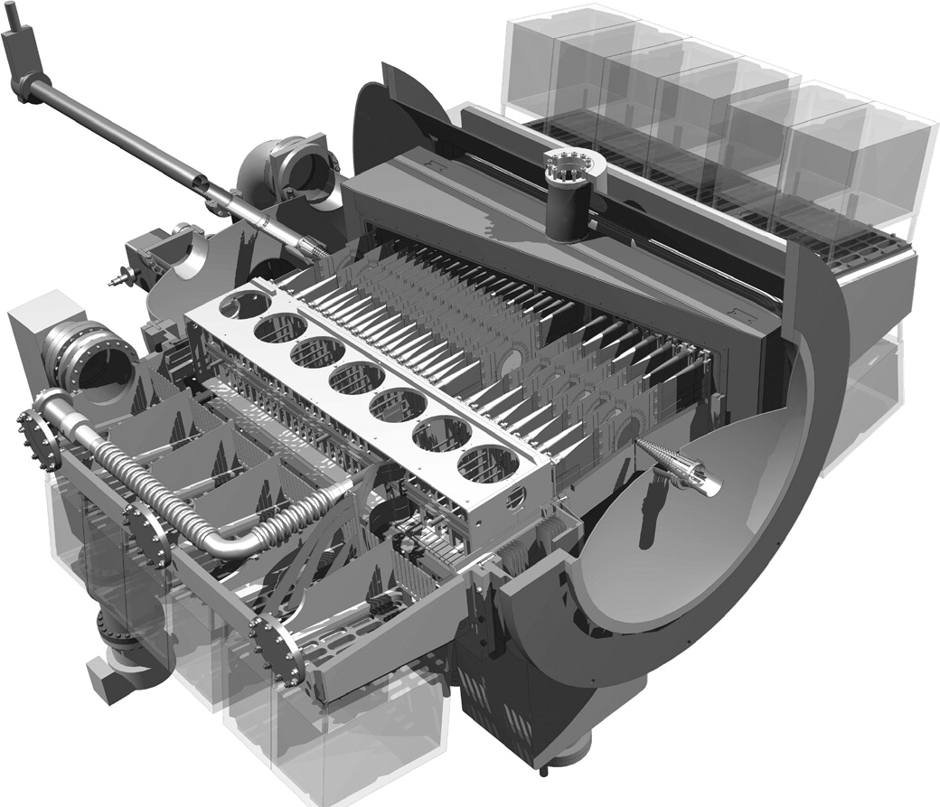
The Vertex Locator (VELO) [2] is the silicon detector surrounding the LHCb interaction point. It is located only 7 mm from the beams during normal operation and measures very precisely the primary vertex and the decay vertices. It consists of two retractable detector halves with 21 silicon micro-strip tracking modules each (figure 1). A module is composed of two -on-n 300 m thick half disc sensors with R and -measuring micro-strip geometry. The detector is operated in vacuum and a bi-phase CO2 cooling system is used. The sensors are readout with the analogue front-end chip (Beetle [3]).
Only when the stable beam flag is raised both halves of the VELO are closed, allowing a small overlap in the inner region, reaching a distance of only 7 mm to the beam line.
1.3 VELO performance
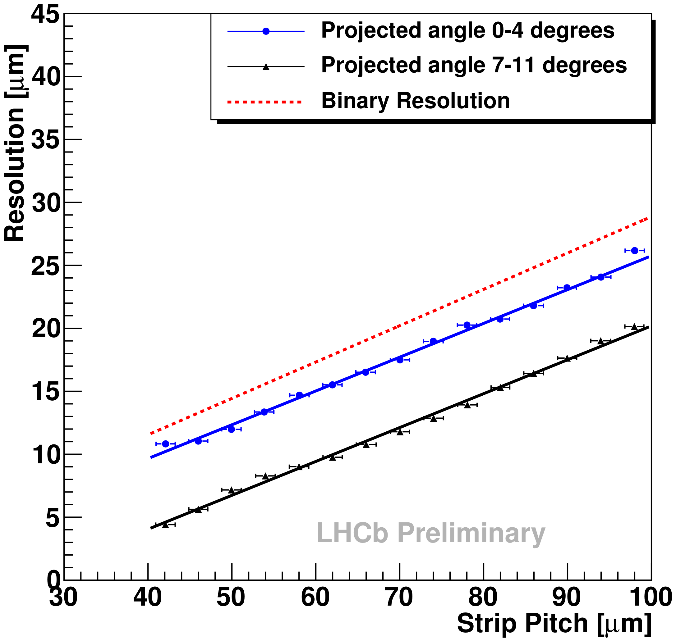
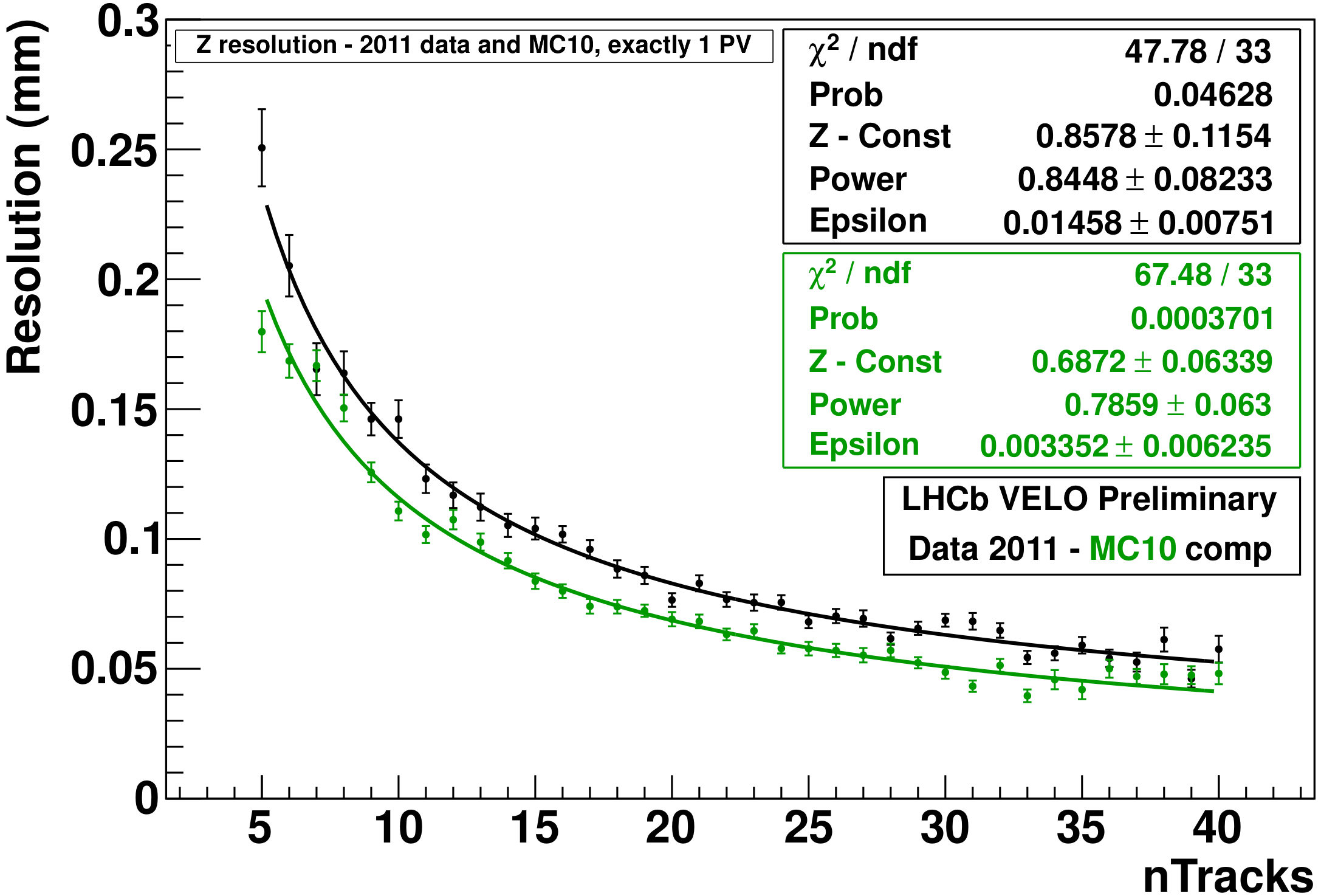
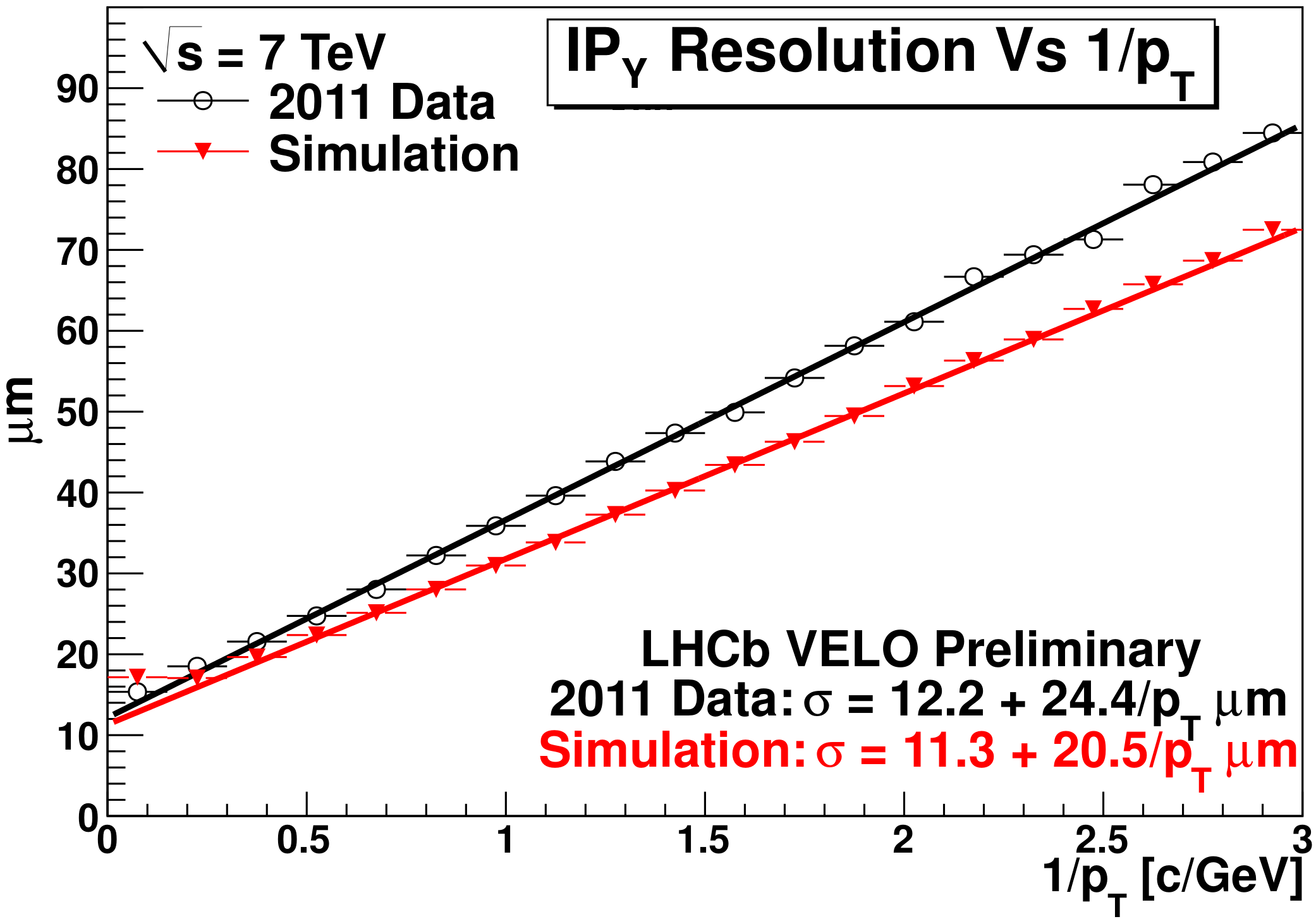
The 1 MHz L0 trigger rate is reduced to a few kHz by full event reconstruction in the computer farm. The VELO plays a crucial role providing vertexing information for this decision. On the tracking and vertexing side, the VELO provides accurate reconstruction of primary and decay vertices, reaching a point resolution of 4 m in the 40 m pitch region at optimal angle (, figure 2a). The primary vertex resolution (PV) is 13 m in the longitudinal direction for about 25 tracks (figure 2b). The final momentum dependent impact parameter resolution (IP) is , where is the transverse momentum in GeV/c (figure 2c). Accurate determination of the IP is very important for LHCb. The relationship between the IP and the PV for a particle is used in the trigger as cut in many physics analysis.
As result, a lifetime resolution of 50 fs was achieved for the flagship channel [4], typical of those channels where the resolution is necessary to resolve fast oscillations. Excellent resolution is also very important for background suppression in rare decay channels.
1.4 Radiation damage
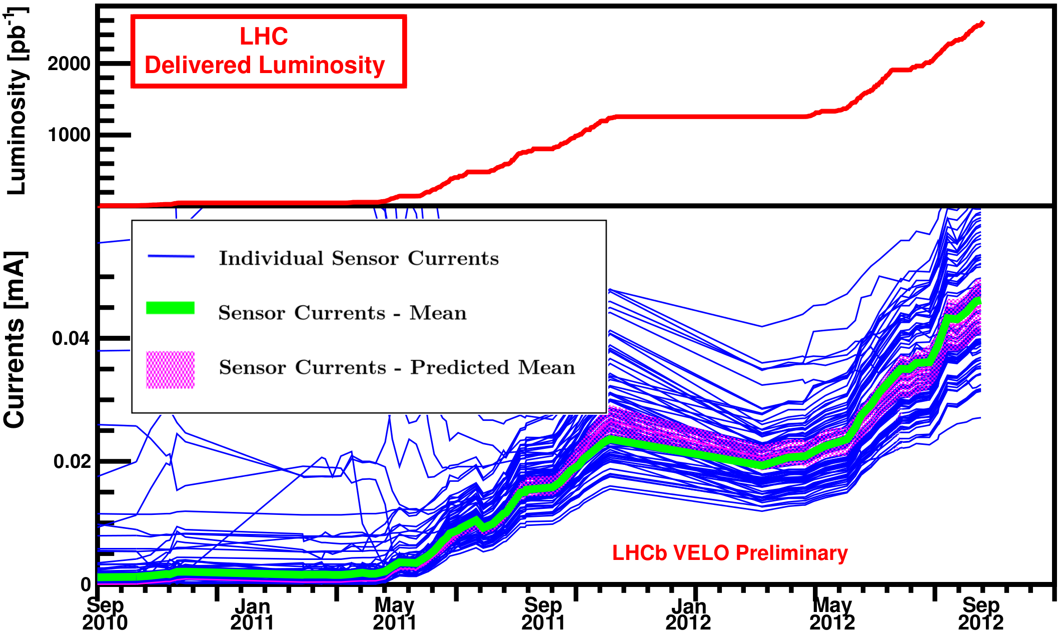
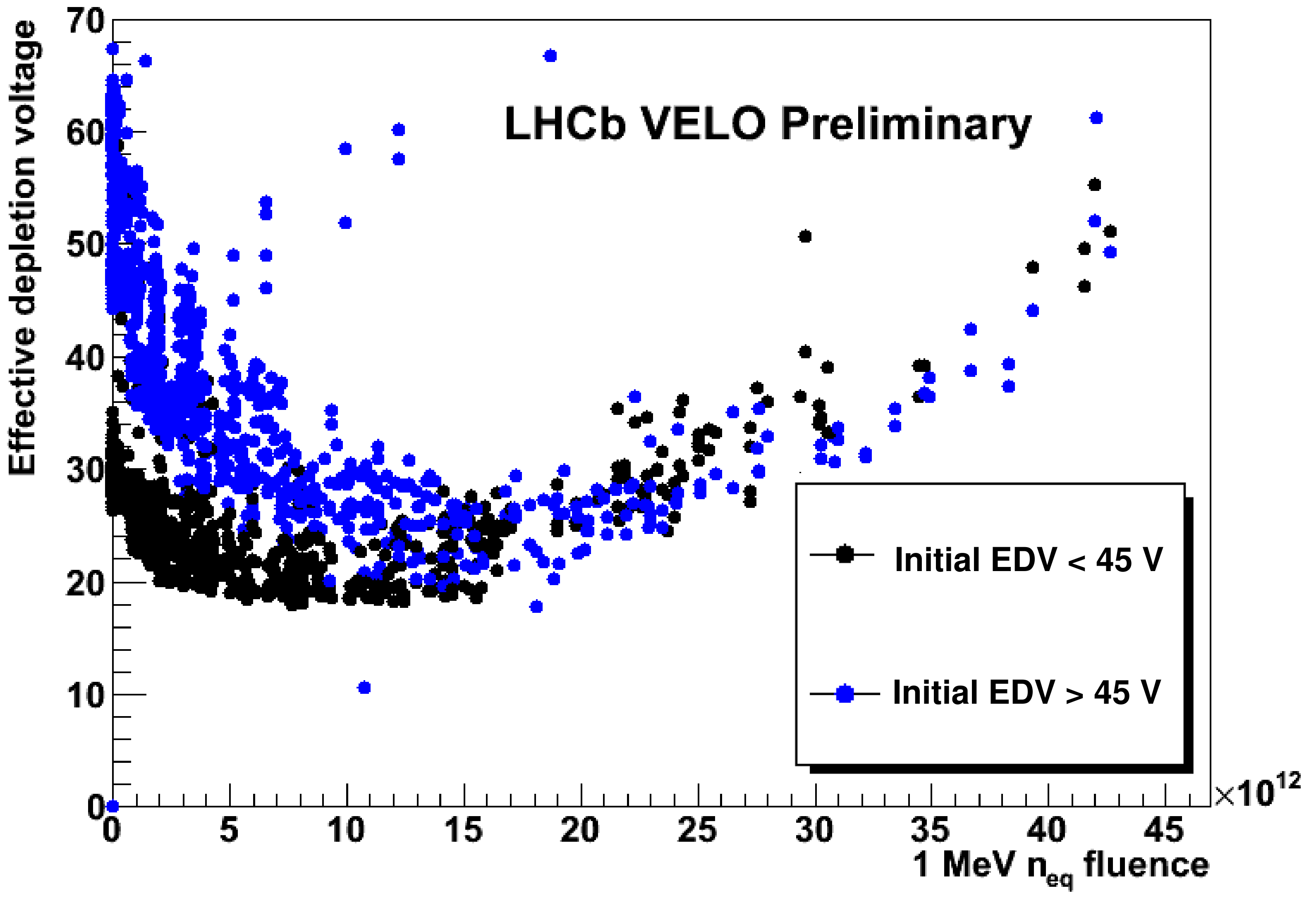
Due to the small distance to the interaction point severe radiation damage is foreseen in the VELO sensors [5], with doses per accumulated . The increase of the leakage current was measured as a function of the delivered luminosity (see figure 3a). The periods with a decrease in the current corresponds to the annealing during shutdown periods or to occasional detector warm ups. The typical current increase is around 1.9 A per 100 delivered. The effective depletion voltage is measured with HV scans during dedicated datataking periods. Figure 3b displays the results of these scans split by detector region and received dose. Most of the innermost parts of the -on-n sensors have already passed through type inversion. Studies of the cluster finding efficiency have revealed a radiation induced charge loss in R-type sensors. For these sensors the mean of the collected charge is lower, and the distribution has experienced deformation due to a growing fraction of clusters with very small charge. The effect has been linked to coupling between routing lines in the second metal layer and the aluminium of the strips in the first metal layer. After irradiation, phantom signals in the inner strips (with readout through lines in the second metal layer) have been detected when the particles cross the outer strips. In the case of the sensors the effect is mitigated because lines in both metalizations are collinear. The exact mechanism and the relationship with radiation damage is under study. For more information about radiation damage in the VELO, see [6, 7].
2 The VELO upgrade
2.1 The LHCb upgrade
The LHCb experiment will record around 1-2 of data per year until end 2017, accumulating in excess of 5 . Afterwards many of the physics channels will still be statistically limited. The LHC is already capable of delivering much higher luminosity to the experiment than the current one, therefore the LHCb has planned an upgrade for 2018 which is independent, but compatible with, the LHC upgrade. After the upgrade the experiment will operate at luminosities up to 2 and will readout collisions at 40 MHz. In these new conditions we expect to collect more than 5 per year, with improvements of up to a factor 2 in the efficiencies in hadronic channels.
2.2 The VELO upgrade
It is a big challenge for the VELO to cope with the requirements of the LHCb upgrade, specially in terms of radiation damage and data bandwidth [8, 9]. These new conditions must be satisfied keeping, or improving, the performance of the current VELO in terms of precision, pattern recognition and impact parameter resolution. Many systems of the current VELO detector, such as the motion system, the vacuum, the power systems (LV/HV) and the evaporative cooling system, will be reused.
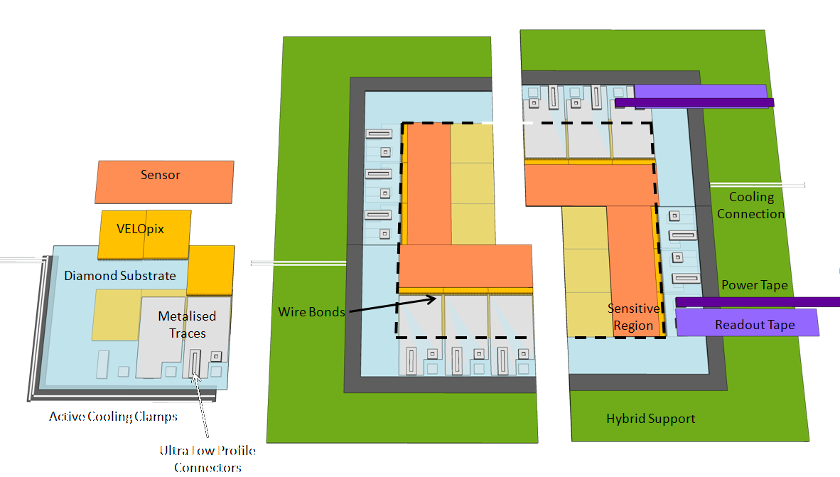
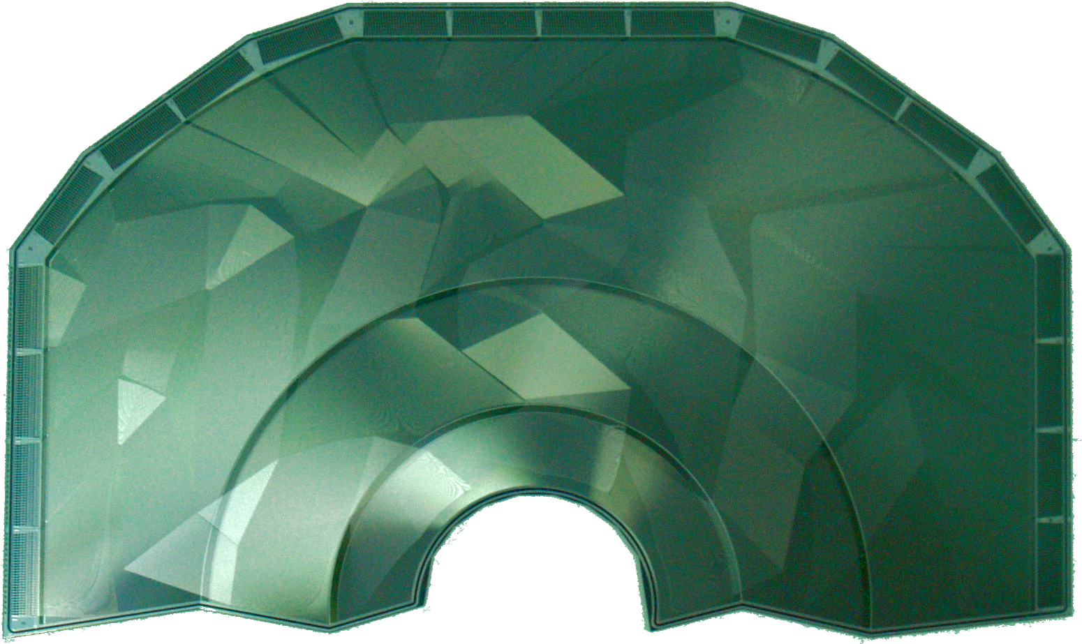
On the sensor side two options are under consideration, pixel sensors with an ASIC based on Medipix/Timepix family (figure 4), and strips sensors with a new and more advanced ASIC (figure 4). Both options imply a completely new module and RF Foil design.
Requirements
One of the main constraints for the VELO upgrade is the bandwidth associated to a triggerless experiment, specially with the increase of the luminosity. The total data rate coming out from the detector will be around 2.4 Tbit/s for the strip option, or 2.8 Tbit/s for the pixel option. The other main issue is the radiation damage, as the upgraded VELO must be able to withstand radiation levels above 400 MRad or 1 MeV .
FE Electronics
Pixel option
The baseline choice for the upgraded VELO is a pixel ASIC called Velopix, which is based on the Timepix3 [10]. Some of the Velopix characteristics are summarized in Table 1. The ASIC will integrate local intelligence at the pixel level for time-over-threshold measurement and sparse readout, on-chip zero suppression and packet-based readout. In addition, Velopix must be immune to single-event upsets in its digital logic. The main difference between TimePix3 and Velopix is that the latter should cope with higher particle flux, hence the bandwidth must be 6 or 7 times greater. The Medipix3 family was designed to be radiation hard, and the Velopix chip will inherit this feature to cope with radiation conditions of the upgraded VELO.
Strips option
The backup solution is the strip sensor with an enhanced design and readout chip. The development of the ASIC is ongoing in synergy with other silicon detectors in LHCb. It will implement embedded solutions such as clustering, sparsification, common mode suppression and pedestal subtraction. A strip design results in a lower material budget than a pixel based solution.
| Pixel array | 256 x 256 |
|---|---|
| Pixel size | 55 m 55 |
| Minimum threshold | 500 |
| Peaking time | < 25 ns |
| Time walk | < 25 ns |
| Measurements | Time-of-Arrival & Time-over-Threshold |
| ToT range | 4 bit (1-2 MIP) |
| ToA resolution / range | 25 ns / 12 bit |
| Count rate | Up to 500 Mhit/s/chip |
| Readout | Continuous, sparse, on-chip clustering |
| Output bandwidth | > 12 Gbit/s |
| Power consumption | < 3 W/chip |
| Radiation hardness | > 500 MRad, SEU tolerant |
Sensors
The baseline option for the sensor is planar silicon with type readout [11]. The challenges for both pixels and strips include coping with a large and very non uniform radiation dose, reducing the material budget and incorporating as narrow as possible guard rings.
For the strip option, sensors should have a minimum pitch of 30 m or below (currently 40 m), 200 m thickness (currently 300 m), n-on-p type, and with a variable pitch in order to keep the same occupancy per strip. For this option, several prototypes with R and design where produced by Hamamatsu, and are currently under characterization in the University of Santiago de Compostela.
In the case of the pixel option, other alternatives than planar sensors are under consideration, like 3D sensors [12] and diamond sensors. Several 3D sensors from CNM were studied during last testbeam campaigns.
Mechanics and cooling
As it was explained in section 2.2 the cooling system for the VELO upgrade will be based on the same evaporative system that is installed in the current VELO. However, two main techniques are being investigated in order to cool the module sensors.
CVD Diamond
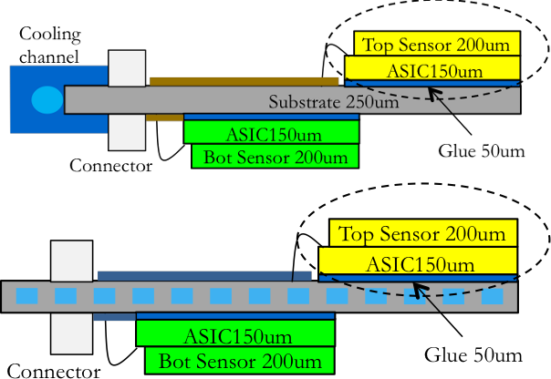
A proposed solution (figure 5a top), and consists of a chemical vapor deposition (CVD) diamond support plus a thermal pyrolitic (TPG) cooling block. The diamond support guarantees a high thermal conductivity, highly robust and low material budget. For this solution the R&D is currently centered on diamond metalization.
Micro-channel
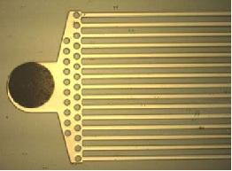
Through etching processes, a set of micro-channels are developed into a silicon substrate [13, 14]. The coolant () is forced to circulate through them at a pressure of 60 bar (figures 5a-bottom and 5b). It is an attractive solution because the channel layout can be adapted to the heat dissipation needs.
RF-Foil
The RF-Foil is the box that encloses the detector halves in a secondary vacuum. It is customized for the sensor layout to allow the placement of sensitive areas at the required distance from the beams, while slightly overlapping in closed configuration. The production of the new RF-Foil is ongoing with milling techniques, and a prototype has been produced for L-shape modules, which is the module for the pixel option. A large R&D is under way to manufacture a full scale prototype within the required specifications.
2.3 The testbeam program
We have built a testbeam telescope with 9 Timepix sensors [15], 8 in ToT111Time over Threshold provides a value proportional to the deposited energy. configuration and the last one in ToA222Time of Arrival provides the time-stamping of the track. This telescope has a point resolution at the Device Under Test (DUT) level of 1.5 m, a time tag resolution of 1 ns and handles a track rate 10 kHz. The Timepix hybrids are connected to an innovative system called RELAXed which is based on FPGAs and can read 4 hybrids in parallel sending the data through an Ethernet connection.
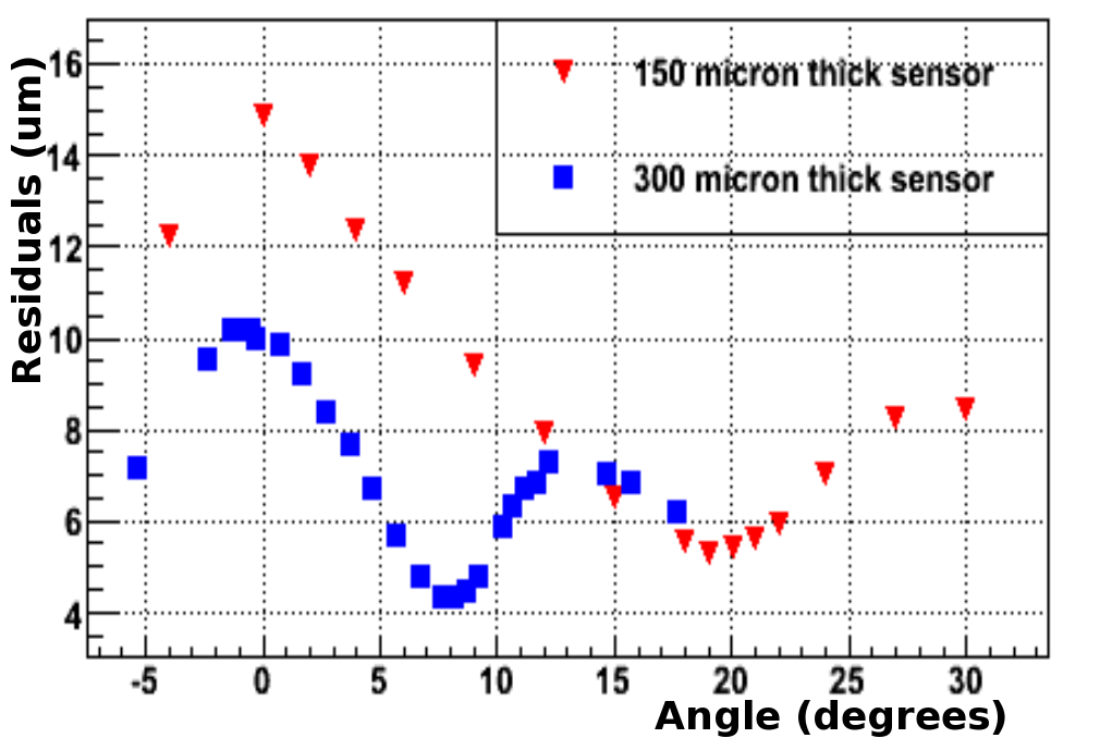
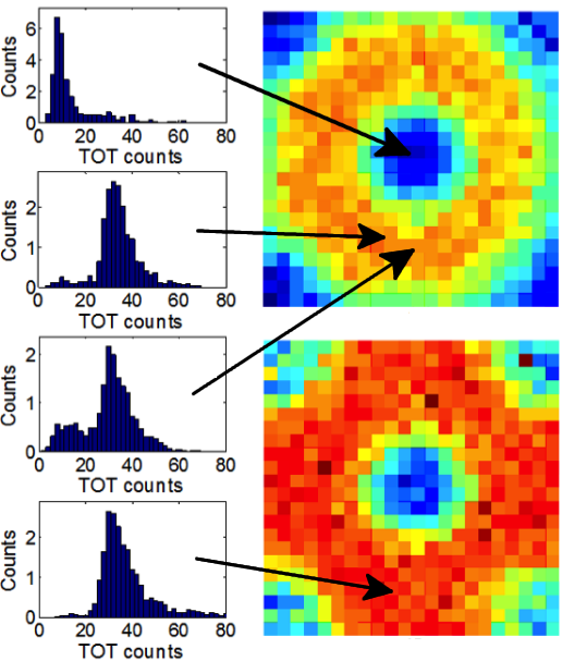
Up to 8 different DUTs were analyzed with this telescope such as irradiated Medipix2 chips, thinned planar sensors (150 m thick) or 3D sensors [16]. In figure 6a a comparison between two planar sensors of 150 m and 300 m thickness is shown. The residual value inform us about the resolution of the reconstructed cluster in the DUT with respect to the extrapolated track given by the telescope, and it changes with the angle and the thickness as expected. In 3D sensors polarization is made between n-type and p-type columns etched into the silicon. Due to this particular geometry, a certain loss of efficiency is expected when a particle crosses the sensor trough a polarization column, as it can be seen in figure 6b.
3 Conclusions
The VELO is operating smoothly under conditions beyond its design. It is a key element in the physics output of the LHCb due to its exceptional performance in terms of vertex and impact parameter resolutions.
As a consequence of the high radiation doses, the VELO sensors have already exhibited radiation damage, and type inversion is observed in the inner regions of the sensors. Nevertheless, the impact in the performance of the detector is not significant up to date.
In 2018 an upgrade of the VELO is planned that should be able to cope with the new requirements of the upgraded LHCb in terms of radiation hardness and readout bandwidth.
Some R&D is still needed in order to select the sensor technology and cooling for the upgraded detector. The candidates are pixels or strips with their associated FE electronics for the sensor and metalized diamond or microchannel for the cooling. The goal is to have confident technologies before 2014 when the production stage will start.
References
- [1] The LHCb Collaboration, The LHCb Detector at the LHC, JINST 3 (2008), no. 08 S08005.
- [2] M. van Beuzekom, Status and prospects of the LHCb vertex locator, Nucl. Instrum. Meth. A 596 (2008), no. 1 21 – 24.
- [3] S. Löchner and M. Schmelling, The Beetle Reference Manual - chip version 1.3, 1.4 and 1.5, Tech. Rep. LHCb-2005-105. CERN-LHCb-2005-105, CERN, Geneva, Nov, 2006.
- [4] G. Krocker, CP violation in mixing with LHCb, Tech. Rep. arXiv:1112.0868, CERN, Dec, 2011. Comments: Proceedings for PIC 2011, Vancouver.
- [5] J. Harrison and A. Webber, Radiation damage in the LHCb VELO, Nucl. Instrum. Meth. A (2012).
- [6] A. H. et al., Use of IT (current vs temperature) scans to study radiation damage in the LHCb VELO, Tech. Rep. LHCb-PUB-2011-021. CERN-LHCb-PUB-2011-021, CERN, Geneva, Oct, 2011.
- [7] P. Rodriguez Perez, Radiation Damage in the LHCb VELO, CERN-Poster-2012-240 (Jul, 2012).
- [8] P. C. et al., The LHCb VELO upgrade, Nucl. Instrum. Meth. A 636 (2011), no. 1, Supplement S185 – S193. 7th International Hiroshima Symposium on the Development and Application of Semiconductor Tracking Detectors.
- [9] P. Collins, The LHCb VELO (VErtex LOcator) and the LHCb VELO upgrade, Nucl. Instrum. Meth. A (2012).
- [10] X. L. et al., Timepix, a 65k programmable pixel readout chip for arrival time, energy and/or photon counting measurements, Nucl. Instrum. Meth. A 581 (2007), no. 1-2 485–494.
- [11] G. C. et al., Enhanced efficiency of segmented silicon detectors of different thicknesses after proton irradiations up to , Nucl. Instrum. Meth. A 624 (2010), no. 2 401 – 404. Proceedings of the 11th European Symposium on Semiconductor Detectors.
- [12] G. P. et al., 3D double sided detector fabrication at IMB-CNM, Nucl. Instrum. Meth. A (2012).
- [13] A. Nomerotski et al., Evaporative cooling for upgraded LHCb VELO detector using microchannels etched in silicon, submitted to Nucl.Instr.Meth (2012).
- [14] A. Mapelli et al., Microfluidic cooling for detectors and electronics, JINST 7 (2012), no. 01 C01111.
- [15] K. A. et al., Charged particle tracking with the Timepix ASIC, Nucl. Instrum. Meth. A 661 (2012), no. 1 31 – 49.
- [16] K. A. et al., Precision scans of the Pixel cell response of double sided 3D Pixel detectors to pion and X-ray beams, JINST 6 (2011), no. 05 P05002.