Robust formation of skyrmions and topological Hall effect in epitaxial thin films of MnSi
Abstract
Magneto-transport properties have been investigated for epitaxial thin films of B20-type MnSi grown on Si(111) substrates. Both Lorentz transmission electron microscopy (TEM) images and topological Hall effect (THE) clearly point to the robust formation of skyrmions over a wide temperature-magnetic field region. New features distinct from those of bulk MnSi are observed for epitaxial MnSi films: a shorter (nearly half) period of the spin helix and skyrmions, and an opposite sign of THE. These observations suggest versatile features of skyrmion-induced THE beyond the current understanding.
pacs:
75.30.Kz, 72.25.Ba, 73.61.At, 75.70.AkThe topological spin texture called skyrmion, in which the constituent spins point in all directions wrapping up a sphere, has recently been observed in the helimagnets with a non-centrosymmetric structure Mühlbauer et al. (2009); Yu et al. (2010, 2011); Tonomura et al. (2012); Seki et al. (2012). This novel magnetic structure has attracted great interest not only for its rich physics related to the quantum Berry phase (skyrmion number) Ye et al. (1999); Bruno et al. (2004); Onoda et al. (2004), but also for its potential application. It is found that the skyrmion motion can be driven by a current density as low as - A/m2 Jonietz et al. (2010); Schulz et al. (2012); Yu et al. (2012), in contrast with the case of magnetic domain walls of conventional ferromagnets, in which the critical current density of - A/m2 is required Myers et al. (1999); Feigenson et al. (2007). This high current-sensitivity may promise the potential application of the skyrmion in the next-generation magnetic recording technique as well as other related spintronic devices.
The skyrmion-hosting B20-type crystal structure is cubic but noncentrosymmetric and hence hosts the Dzyaloshinskii-Moriya (D-M) interaction. This antisymmetric spin exchange interaction competes with symmetric Heisenberg exchange and Zeeman interactions, producing rich magnetic structures, such as helical (proper screw) spin structure Ishikawa et al. (1976); Bak and Jensen (1980), conical spin structure Ishikawa et al. (1976); Grigoriev et al. (2006), and field-induced ferromagnetism. The skyrmion spin texture, which is a superposition of three helices perpendicular to the external magnetic field , is also a consequence of the competition but can be found only in quite a limited temperature-magnetic field (-) region (so-called phase) for bulk crystals Mühlbauer et al. (2009). The coverage of skyrmion phase, however, turns out to be greatly enlarged in thin plates Yi et al. (2009); when is applied normal to film planes, the extended skyrmion phases have been observed by Lorentz TEM in free-standing thin plate specimens, the thickness of which are reduced to 100 nm by ion-milling the bulk samples such as Fe0.5Co0.5Si Yu et al. (2010), FeGe Yu et al. (2011), MnSi Tonomura et al. (2012), and insulating multiferroic Cu2OSeO3 Seki et al. (2012).
In the light of both fundamental research and application, epitaxial growth of these B20 compound thin films is more beneficial, because the thickness can be better controlled, the transport properties can be precisely measured, and the desired patterning for the device fabrication is easy to implement. Despite the intensive effort in fabricating epitaxial B20 thin films, such as of MnSi Magnano et al. (2006); Higashi et al. (2009); Azatyan et al. (2011); Magnano et al. (2010); Karhu et al. (2010, 2011), no compelling evidence of the skyrmion formation has yet been obtained. A recent study on the fabrication of FeGe/Si(111) thin films has argued that the topological Hall effect (THE) exists over a wide - region Huang and Chien (2012). The THE itself is not limited to the skyrmion spin structure alone Bruno et al. (2004); Onoda et al. (2004) but emergent in other noncoplanar spin systems as well, therefore the one-to-one correspondence between skyrmion formation and THE in epitaxial thin films is to be evidenced. In this paper, we report the realization of high-quality epitaxial MnSi/Si(111) thin film and demonstrate skyrmion-derived THE through the combination of transport measurements and the real-space observations by Lorentz TEM.

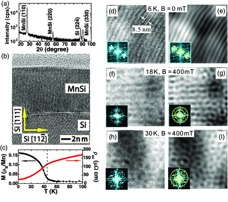
Our optimized scheme of the epitaxial growth of MnSi(111) thin film is to start with depositing 4 monolayer Mn at room temperatures onto Si(111)-77 surface followed by annealing at 200 ∘C to form a seed layer of MnSi, then depositing Mn and Si at room temperature either by co-evaporation or by repeating Mn/Si sandwich layers, and finally annealing it at 300-400 ∘C. The single-phase nature was checked by the grazing-incident X-ray diffraction, which shows no detectable impurity phase [Fig. 1(a)]. High crystalline quality is also confirmed by cross-section TEM image [Fig. 1(b)].
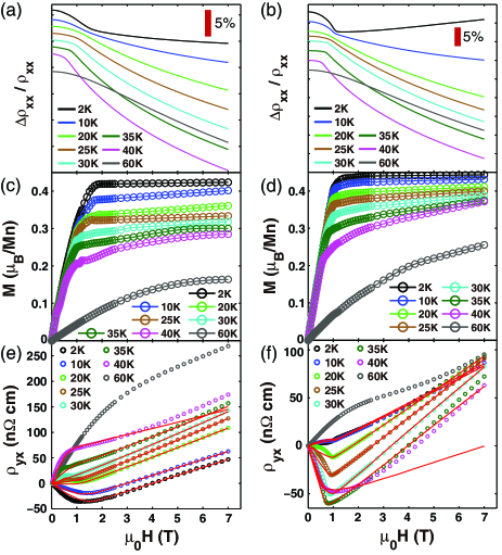
The transition temperature of the 10 nm MnSi film is determined to be 45 K from the temperature profile of field-cooling magnetization and zero-field cooling longitudinal resistivity - [Fig. 1(c)]. The of 50 nm film is found almost identical with that of the 10 nm film. The present is appreciably higher than those of bulk MnSi (29.5 K) and free-standing thin film sliced off from the bulk (22.5 K for the 50 nm film), perhaps due to tensile strain induced by 3% lattice mismatch between the epitaxial MnSi film and Si(111) substrate Karhu et al. (2010). Below , a sufficiently large field aligns all the spins and turns the system into the induced ferromagnetic (spin-collinear) state. This transition manifests itself as the kink-like behavior in - and - curves [Figs. 2(c)-(f)]. The saturated magnetization () at 2 K, which is derived as extrapolating from high field to zero field, is found to be per Mn atom, in good agreement with the reported value for bulk MnSi Lee et al. (2007).

Figures 1(d)-(l) show representative Lorentz TEM images on the 10 nm MnSi/Si(111) film. At 6 K under zero external field, the helical structure is clearly observed as the alternating bright and dark stripes in a Lorentz TEM image [Fig. 1(d)]. The vortex-like skyrmions [bright or dark dots shown in Figs. 1(f) and (h)] can be observed at higher temperatures (18 K and 30 K) under 400 mT normal to the film. For clarity, we also present the filtered images [Figs. 1(e), 1(g), and 1(l)], which are reconstructed from the filtered magnetic reflection via the fast-Fourier-transform. Here we note that the Lorentz TEM observation reveals remarkable differences from previous results in bulk MnSi Ishikawa et al. (1976); Grigoriev et al. (2006); Mühlbauer et al. (2009) and the free-standing thin film Tonomura et al. (2012). First, the period of helical structure () is 8.5 nm in the 10 nm MnSi film [illustrated by the arrows in Fig. 1(d)], about half of that in the bulk specimen (18 nm). This discrepancy likely originates from different exchange coupling strengths, because is determined by the ratio , where and are the Heisenberg and D-M exchange couplings, respectively Bak and Jensen (1980); Nakanishi et al. (1980); the tensile strain from the substrate may alter the magnetic parameter, or substantially increase . Second, the skyrmions observed in the epitaxial 10 nm film show little sign of long-range order (i.e., the hexagonal skyrmion crystal) and form a glassy state. This feature invokes the presence of disorder, which may come from slight off-stoichiometry of Mn/Si and/or lattice defects. These observations point to a sort of hierarchical nature of skyrmion formation, i.e., the local skyrmion formations themselves are robust against disorder, while their long-range crystalline packing may be prevented by the presence of disorder.
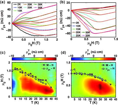
To see how the skyrmion formation affects transport properties, we looked into the field dependence of Hall resistivity of the 10 nm and 50 nm films. The results are shown in Figs. 2(e) and (f) [see Figs. 4(a) and (b) for magnified views in the low-field region]. For the both films, hamp-like anomalies can be clearly seen between 15 K and 35 K when , i.e., in accord with the - region of skyrmions observed by the Lorentz TEM. We therefore ascribe this anomaly to the THE induced by the skyrmion spin texture. In general, the total Hall resistivity can be expressed as the sum of various contributions: , where is the normal Hall coefficient, the anomalous Hall resistivity, and the topological Hall resistivity. In Figs. 2(e), 2(f), 4(a), and 4(b), the THE signal clearly coexists with a large background of normal Hall effect and anomalous Hall effect (AHE). To extract the THE quantitatively, should be singled out from first. Here we analyze by employing the following scaling Tian et al. (2009); Ye et al. (2012); Shitade and Nagaosa (2012):
| (1) |
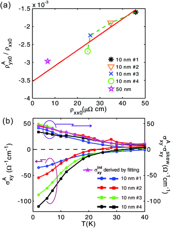
where the terms with , , and correspond to the skew scattering, the side jump, and the intrinsic contribution respectively, while stands for the residual resistivity. We derived by extrapolating in a high field region (linear fitting from 9 T to 5 T) to zero field. When 0 K, both and take their residual values, and thus Eq. (1) reduces into a simpler equation, . Accordingly, we show in Fig. 3(a) the result obtained at 2 K from the four 10 nm-thick samples with different values gro . From the linear fitting, is determined to be . The same value seems applicable to 50 nm film as well [see Fig. 3(a)].

In terms of conductivity, Eq. (1) can be written equivalently as Tian et al. (2009); Shitade and Nagaosa (2012):
| (2) |
where again the terms with , correspond to the skew scattering and the side jump respectively, while the last term denotes the intrinsic anomalous Hall conductivity . It is straightforward to see that . We plot now in Fig. 3(b) both and as a function of temperature for all the 10 nm-thick samples. It is interesting to observe that while scatters among different samples especially at low temperatures, the temperature variations of derived reduce to a single universal, sample-independent curve. This feature presumably implies that the sample-dependent extrinsic term is negligibly small, i.e., Ye et al. (2012).
The total Hall resistivity can therefore be expressed as
| (3) |
For , is supposed to be zero, because the induced ferromagnetism has no spin chirality. Hence, and can be determined, respectively, from the intercept and the slope of linear fitting of vs (not shown), with the value as determined above. In this analysis, we used the - curves shown in Figs. 2(a) and (b). The fitted results of are shown as the red solid lines in Figs. 2(e)(f) and Figs. 4(a)(b). As a crosscheck we also plotted derived from the fitting result as in Fig. 3(b) and found that the temperature profile of obtained reasonably coincides with as derived above. In this way, we can extract from the difference between the total Hall resistivity and the fitted curve below .

In the following, we discuss in the light of the skyrmion formations. To see the global feature of , we present the contour mapping of derived as a function of and [Figs. 4(c) and (d) for the 10 nm and 50 nm films, respectively]. A finite is found in both films for K and , consistent with the Lorentz TEM observation, which finds the skyrmion state at 18 K and 30 K under mT. We can thus link the onset of a positive to the formation of the skyrmion state, and consequently Figs. 4(c) and (d) can be regarded as the magnetic phase diagrams of MnSi thin films. Obviously, the skyrmion state as evidenced by the emergence of THE is stabilized over a broad region in the - plane, spanning from 10 K to and occupying almost all the region below except near zero field; this is in sharp contrast to the small phase region in bulk MnSi Mühlbauer et al. (2009); Neubauer et al. (2009). The maximum value of in the epitaxial thin films is about 10 ncm, approximately twice as large as that in bulk MnSi (-4.5 ncm) Neubauer et al. (2009), albeit the signs are opposite, which will be discussed later. Furthermore, for both the 10 nm and 50 nm films, the sign of flips from positive to negative when K. This behavior is more prominent in the 10 nm film [see the raw data shown in Fig. 4(a)], where the maximum magnitude of (about -7.8 ncm) is comparable to the that of the positive observed at higher temperatures. Unfortunately this temperature range ( K) cannot be reached in our Lorentz TEM setup. The spin texture in this low temperature region requires further investigations.
The sign of is considered to depend on the spin polarization () of charge carriers. The band structure calculation of B20 bulk MnSi indicates that the net spin polarization of the electron state near Fermi surface is very sensitive to the position of Fermi level Jeong and Pickett (2004); Hortamani et al. (2008), and the sign of may be inverted even within the accuracy of the calculation Jeong and Pickett (2004). The density of states near Fermi level is overwhelmingly contributed by -electrons Jeong and Pickett (2004), which are rather localized, and the contributions of itinerant -band is rather small; this feature makes the calculation of of charge carriers even more delicate. All these facts suggest that the may be affected largely by a small change in the band structure, which could be induced, for example, by the tensile strain or even by the temperature variations. The large (by half) change of the helical period in the present thin film may also signal the modification of the electronic structure. This may explain the discrepancy of the sign of between in epitaxial MnSi film and in bulk MnSi.
In conclusion, we have succeeded in fabricating high-quality epitaxial MnSi/Si(111) thin films that host the skyrmion phase. A combination of the Lorentz TEM and measurement of topological Hall effect reveals that the skyrmion phase is extended over a much wider temperature-magnetic field range than the skyrmionic phase of bulk MnSi. The results for the 10 nm and 50 nm MnSi films show consistently that the sign of topological Hall resistivity is opposite to that in bulk MnSi, which may reflect the sign change of the conduction electron spin polarization affected by the epitaxial lattice strain, possible nonstoichiometry, and temperature-variation.
The authors wish to thank N. Nagaosa for fruitful discussions. This work was partially supported by “KAKENHI”.(Nos. 24224009 and 24684020) from the MEXT and by the Japan Society for the Promotion of Science (JSPS) through its “Funding Program for World-Leading Innovative RD on Science and Technology (FIRST Program)”.
References
- Mühlbauer et al. (2009) S. Mühlbauer, B. Binz, F. Jonietz, C. Pfleiderer, A. Rosch, A. Neubauer, R. Georgii, and P. Böni, Science 323, 915 (2009).
- Yu et al. (2010) X. Z. Yu, Y. Onose, N. Kanazawa, J. H. Park, J. H. Han, Y. Matsui, N. Nagaosa, and Y. Tokura, Nature 465, 901 (2010).
- Yu et al. (2011) X. Z. Yu, N. Kanazawa, Y. Onose, K. Kimoto, W. Zhang, S. Ishiwata, Y. Matsui, and Y. Tokura, Nat. Mat. 10, 106 (2011).
- Tonomura et al. (2012) A. Tonomura, X. Z. Yu, K. Yanagisawa, T. Matsuda, Y. Onose, N. Kanazawa, H. S. Park, and Y. Tokura, Nano. Lett. 12, 1673 (2012).
- Seki et al. (2012) S. Seki, X. Z. Yu, S. Ishiwata, and Y. Tokura, Science 336, 198 (2012).
- Ye et al. (1999) J. Ye, Y. B. Kim, A. J. Millis, B. I. Shraiman, P. Majumdar, and Z. Tešanović, Phys. Rev. Lett. 83, 3737 (1999).
- Bruno et al. (2004) P. Bruno, V. K. Dugaev, and M. Taillefumier, Phys. Rev. Lett. 93, 096806 (2004).
- Onoda et al. (2004) M. Onoda, G. Tatara, and N. Nagaosa, J. Phys. Soc. Jpn. 73, 2624 (2004).
- Jonietz et al. (2010) F. Jonietz, S. Mühlbauer, C. Pfleiderer, A. Neubauer, W. Münzer, A. Bauer, T. Adams, R. Georgii, P. Böni, R. A. Duine, et al., Science 330, 1648 (2010).
- Schulz et al. (2012) T. Schulz, R. Ritz, A. Bauer, M. Halder, M. Wagner, C. Franz, C. Pfleiderer, K. Everschor, M. Garst, and A. Rosch, Nat. Phys. 8, 301 (2012).
- Yu et al. (2012) X. Z. Yu, N. Kanazawa, W. Z. Zhang, T. Nagai, T. Hara, K. Kimoto, Y. Matsui, Y. Onose, and Y. Tokura, Nat. Commun. 3, 988 (2012).
- Myers et al. (1999) E. B. Myers, D. C. Ralph, J. A. Katine, R. N. Louie, and R. A. Buhrman, Science 285, 867 (1999).
- Feigenson et al. (2007) M. Feigenson, J. W. Reiner, and L. Klein, Phys. Rev. Lett. 98, 247204 (2007).
- Ishikawa et al. (1976) Y. Ishikawa, K. Tajima, D. Bloch, and M. Roth, Solid State Commun. 19, 525 (1976).
- Bak and Jensen (1980) P. Bak and M. H. Jensen, J. Phys. C 13, L881 (1980).
- Grigoriev et al. (2006) S. V. Grigoriev, S. V. Maleyev, A. I. Okorokov, Y. O. Chetverikov, P. Böni, R. Georgii, D. Lamago, H. Eckerlebe, and K. Pranzas, Phys. Rev. B 74, 214414 (2006).
- Yi et al. (2009) S. D. Yi, S. Onoda, N. Nagaosa, and J. H. Han, Phys. Rev. B 80, 054416 (2009).
- Magnano et al. (2006) E. Magnano, E. Carleschi, A. Nicolaou, T. Pardini, M. Zangrando, and F. Parmigiani, Surface Science 600, 3932 (2006).
- Higashi et al. (2009) S. Higashi, P. Kocán, and H. Tochihara, Phys. Rev. B 79, 205312 (2009).
- Azatyan et al. (2011) S. Azatyan, O. Utas, N. Denisov, A. Zotov, and A. Saranin, Surface Science 605, 289 (2011).
- Magnano et al. (2010) E. Magnano, F. Bondino, C. Cepek, F. Parmigiani, and M. C. Mozzati, Appl. Phys. Lett. 96, 152503 (2010).
- Karhu et al. (2010) E. A. Karhu, S. Kahwaji, T. L. Monchesky, C. Parsons, M. D. Robertson, and C. Maunders, Phys. Rev. B 82, 184417 (2010).
- Karhu et al. (2011) E. A. Karhu, S. Kahwaji, M. D. Robertson, H. Fritzsche, B. J. Kirby, C. F. Majkrzak, and T. L. Monchesky, Phys. Rev. B 84, 060404 (2011).
- Huang and Chien (2012) S. X. Huang and C. L. Chien, Phys. Rev. Lett. 108, 267201 (2012).
- Lee et al. (2007) M. Lee, Y. Onose, Y. Tokura, and N. P. Ong, Phys. Rev. B 75, 172403 (2007).
- Nakanishi et al. (1980) O. Nakanishi, A. Yanase, A. Hasegawa, and M. Kataoka, Solid State Commun. 35, 995 (1980).
- Tian et al. (2009) Y. Tian, L. Ye, and X. Jin, Phys. Rev. Lett. 103, 087206 (2009).
- Ye et al. (2012) L. Ye, Y. Tian, X. Jin, and D. Xiao, Phys. Rev. B 85, 220403 (2012).
- Shitade and Nagaosa (2012) A. Shitade and N. Nagaosa, J. Phys. Soc. Jpn. 81, 083704 (2012).
- (30) The 10 nm-thick film was MBE-grown by codepositing Mn and Si on MnSi seed-layer at 270∘C. The seed-layer was prepared as described in the text. The 10 nm-thick films were fabricated by preparing Mn/Si layers on the seed-layer at room temperature followed by annealing as described in the text, where the layers of and were prepared by depositing sandwich structures of repeating Mn/Si layers in 4 ML(monolayer)/4 ML and 12 ML/12 ML respectively, and the layer of by codepositing Mn and Si simultaneously at room temperature. The 50 nm-thick film was fabricated in the similar way as the 10 nm-thick film .
- Neubauer et al. (2009) A. Neubauer, C. Pfleiderer, B. Binz, A. Rosch, R. Ritz, P. G. Niklowitz, and P. Böni, Phys. Rev. Lett. 102, 186602 (2009).
- Jeong and Pickett (2004) T. Jeong and W. E. Pickett, Phys. Rev. B 70, 075114 (2004).
- Hortamani et al. (2008) M. Hortamani, L. Sandratskii, P. Kratzer, I. Mertig, and M. Scheffler, Phys. Rev. B 78, 104402 (2008).