Mechanism to Generate a Two-Dimensional Electron Gas at the Surface of the Charge-Ordered Semiconductor BaBiO3
Abstract
In this work, we find by means of first-principles calculations a new physical mechanism to generate a two-dimensional electron gas, namely, the breaking of charge ordering at the surface of a charge ordered semiconductor due to the incomplete oxygen environment of the surface ions. The emergence of the 2D gas is independent of the presence of oxygen vacancies or polar discontinuities; this is a self-doping effect. This mechanism might apply to many charge ordered systems, in particular, we study the case of BaBiO3(001). Our calculations show that the outer layer of the Bi-terminated simulated surface turns more cubic- like and metallic while the inner layers remain in the insulating monoclinic state that the system present in the bulk form. On the other hand, the metallization does not occur for the Ba termination, a fact that makes this system appealing for nanostructuring. Finally, in view of the bulk properties of this material under doping, this particular finding sets another possible route for future exploration: the potential scenario of 2D superconductivity at the BaBiO3 surface.
pacs:
73.20.-r, 71.45.Lr, 71.30.+h, 71.15.MbWhen the extension of a semiconductor crystal is not assumed infinite, due to the presence of a surface or an interface with another material, the bulk electronic wave functions are altered giving rise to intrinsic surface states that are allowed to lie in the band gap. These surface states might have metallic behavior conforming a two-dimensional electron gas (2DEG). The emergence of these 2DEGs at the interface of conventional semiconductors has been at the basis of device development and engineering in the field of electronics for more than 50 years. The physical mechanism behind the generation of these conducting states may have different origins depending on the system. At clean undoped semiconducting surfaces, they can be attributed to the unpaired electrons of dangling bond states within the band gap, while, in semiconductor heterojunctions, band-bending is a determinant factor for 2DEG formationsemiconductor .
Since the last decade, due to the progress made in the heteroepitaxial growth of complex oxides, it has become possible to generate 2DEGs at oxide interfaces Ohtomo and Hwang (2004). This fact brought about a wide variety of phenomena such as superconductivityN. Reyren et al (2007), magnetic-orderA. Brinkman et al. (2007), electron correlation-driven effectsPentcheva and Pickett (2007), among others, awakening the interest on both fundamental issues and their future technological applications in the field of oxide electronics. It is nowadays still an issue of intense debate what is the origin of the 2DEGs at these oxide interfaces. One point of view ascribes them to polar/non polar interfaces and is based on the polar ”catastrophe” model that proposes an electronic reconstruction to compensate the growing dipole moment as the number of polar layers increases. Another invoked mechanism is the presence of oxygen vacancies in the substrate. Each scenario explains part of the storyOhtomo and Hwang (2004); A. Kalabukhov et al. (2007); G. Herranz et al. (2007); M. Basletic and et al. (2008) and, probably, a complete understanding of the intrinsic nature of the 2DEG formation is highly dependent on the materials involved and on the experimental set up. Recently, it has been shown that a 2DEG can also be generated in a simpler context, namely, at the vacuum-cleaved surface of SrTiO3. In this case, a metallic gas is formed independently of the oxide bulk carrier densities, opening the way towards novel means of 2DEG generation at the surface of transition-metal oxidesA. F. Santander-Syro at al. (2011). In this case, the presence of oxygen vacancies is suggested to lie behind the emergence of metallic surface states.
In this work, based on Density Functional Theory(DFT)-calculationsHohenberg and Kohn (1964), we propose not only a new candidate able to sustain a confined electron gas but also a new physical mechanism to generate it, that is different from the ones invoked until now. We show, namely, that a 2DEG is formed at the (001) surface of insulating BaBiO3 as a consequence of a charge order disruption. No external factors, such as polar discontinuities or oxygen vacancies, are necessary to obtain, in this case, the 2DEG except for the Bi- terminated surface itself. The surface generated carrier densities are quite high and of the same order of magnitude as the ones measured at other oxide interfaces or clean surfaces. This phenomenon might be present in many other charge ordered materials as will be discussed later.
In order to understand the nature of our finding we briefly describe the phase diagram of bulk BaBiO3. At high temperature (T 750 K) it is a cubic perovskite exhibiting metallic behaviour. Formally, one would expect each bismuth to have a valence 4+. However, Bi is a typical valence-skipping atom, and even in the high temperature metallic phase, it presents charge disproportionation. At lower temperatures, this disproportionation couples to the tilting of the BiO6 octahedra. The crystal structure goes through a rhombohedral phase (750K T 405K), becoming monoclinic for T 405KCox and Sleight (1976). The charge disproportionation together with the structural distortion are further enhanced giving rise to a formal Bi5+- Bi3+ charge-ordered Peierls-like insulator in the low temperature monoclinic phase. The oxygen octahedra around the Bi ions present alternating breathing-in and breathing-out structural instabilities. Being the electronic properties of this material fascinanting by themselves, the discovery of high-Tc superconductivity in doped BaBiO3A. W. Sleight et al. (1975); R. J. Cava et al (1988) makes this system even more intriguing and interesting. It has been shown that upon doping, the monoclinic phase turns cubic or tetragonal (depending on the dopant) and metallic, exhibiting superconductivity with Tc’s as high as 30K. Much of the understanding of the electronic structure and structural properties of both, the parent BaBiO3 and the doped compounds, has been accomplished by means of first principle calculationsMattheiss ; early-DFT ; Thonhauser and Rabe (2006). In this material, the physics is dominated by spatially quite extended Bi(s)-O(p) orbitals. In the absence of important correlation effects, as in typical d or f electron systems, much progress has been made from early local-density approximation (LDA) calculationsPerdew and Zunger (1981) based on DFT.
 |
 |
Calculations using LDA (or its gradient corrections GGAJ. P. Perdew et al. (1996)) could already explain the splitting of the Bi(s)-O(p) band around EF due to Peierls- like distortions that are switched on, in particular, by the breathing instabilityThonhauser and Rabe (2006). These calculations account, then, for the charge disproportionation and its relation to the structural distortions in the monoclinic phase. LDA(GGA) results predict a semi-metallic behaviour, however, it is well known that BaBiO3 bulk presents an indirect gap whose experimental reported value goes from 0.2 eV to 1.1 eVNot (a). More recently it has been shown that in order to open the indirect gap and describe quantitatively the structural properties and the insulating behaviour of this phase of bulk BaBiO3, it is necessary to go beyond standard DFT approaches, for instance by using hybrid functionals that combine a fraction of non-local exact exchange with local or semilocal approximationsC. Franchini et al. (2010).
In this contribution, the theoretical study of the (001) surface of BaBiO3 is faced for the first time. We perform first principles DFT calculations and take care of the gap problem by cross-checking the results with functionals that go beyond LDA or GGA such as the modified Becke-Johnson potential (mBJ) Tran and Blaha (2009) and the Heyd-Scuseria-Ernzerhof hybrid functional (HSE) J. et al. (2003). The mBJ correction is done within the Wien2k code P. Blaha et al. (2002) and the HSE functional within the VASP package Kresse and Furthmüller (1996). In the Supplementary material we show that the main physical findings are obtained using either GGA, mBJ or HSE functionals. The surfaces are modeled by supercells with different slab thicknesses. We consider slabs composed by 9 to 15 layers that are stacked following the monoclinic crystal structure with both Ba- and Bi- terminated situations in the (001) direction. To avoid the interaction between oppossite surfaces, they are separated in the z direction by an empty space volume ranging from 9 to 21. The supercells have two inversion symmetric surfaces for simplicity. All internal atomic positions are allowed to relax.
Our caculations indicate that Bi- terminated BaBiO3 turns metallic while the Ba-terminated surface remains insulating as in the bulk (monoclinic phase). The results obtained for different supercells with different number of layers are qualitatively the same in the corresponding termination. The comparison among different slabs is useful to detect finite size effects (as described below).
 |
 |
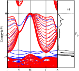
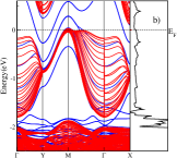
In Fig. 1 we show the bandstructure and total densities of states (DOS) for a Ba- and a Bi- terminated slab, a) and b), respectively. These bandstructures correspond to slabs with 11 and 13 layers. In the bandstructure plots, the bulk projected bands (in red) in the (001) direction are shown on top the ones coming from the slab calculations (in blue). It can be clearly seen that in the first case, the system behaves as an insulator, while in the second one there are several surface states crossing EF, giving rise to metallic behaviour. In Fig. 1 a), the bands above the Fermi level have mainly Bi5+-O character and the ones below mainly Bi3+-O one. The set of bands below -2.0 eV have mostly O-p states with a significant Bi-6s weight. In Fig. 1 b), there are four bands (surface states) crossing EF that basically come from the Bi surface atoms which are strongly mixed with O-p states. There are also visible surface states around -2.0 eV due to this hybridization. There is a tiny pocket around the M point which is due to a finite size effect. The contribution of this pocket to the Fermi surface increases considerably for thinner slabs.
The metallization of the Bi- terminated surface is a consequence of the incomplete octahedral environment of the Bi ions, which produces a rearrangement of the charge distribution suppressing the charge ordering at that BiO2 plane. This suppression of the disproportionation is, in fact, partial but strong enough to turn the system metallic, as it is the case in the high temperature cubic phase of bulk BaBiO3. On the other hand, for Ba termination, the oxygen octahedral environment of all Bi ions is complete and, the charge ordering is, then, not affected in any of the BiO2 planes. There is, indeed, a slight charge redistribution among the O atoms at the BaO surface plane, which has no effect on the insulating behavior of the whole system.
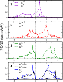
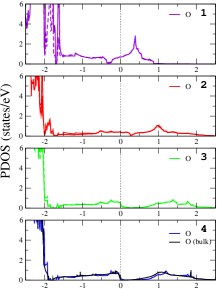
In order to trace the origin of this metallicity, in Fig. 2 we plot the DOSs (obtained with the mBJ correction) projected onto the BiO2 planes for the Bi- terminated 13 layers slab. The BaO layers are skipped for the sake of simplicity. The bulk projected DOSs are plotted on top of the ones of layer 4 (in black), for comparison. The effects of charge disproportionation in the bulk can be clearly observed within the [-2 eV, 2 eV] energy range. There are quasi-symmetrically distributed occupied and empty 6s bands around EF, presenting the Bi3+ ions mostly occupied states and the Bi5+ ions mostly empty ones. The important Bi(6s)-O(p) hybridization is clearly appreciable in the O projected DOS.
Our slab results show that already the third Bi layer from the surface, has a bulk like projected DOS. The slight downward shift of the Fermi level for layers 3 and 4, as compared to the bulk, is again due to a finite size effect. The thinner the slab, the larger the downward shift of EF into the 6s valence bands. The behaviour of the Bi-6s and O states of the surface and subsurface Bi- layers (labeled as and ) is qualitatively different to what happens in the deeper Bi planes. In layers 1 and 2 there is an effective charge transfer from the originally Bi3+ to the Bi5+ ions. The system turns, in this way, metallic and this metallicity is mainly confined to the two outer BiO2 planes of the Bi- terminated BaBiO3. For the thinner film considered, namely the 9 layers slab (not shown in Fig. 2), the confinement is less effective but still the metallization is predominantly at the outer layers.
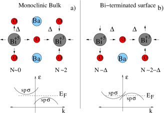
In Fig. 3 we show a scheme of the physical mechanism explaining the 2DEG formation. The bandstructure of the bulk monoclinic phase presents one fully occupied and one unoccupied band per fomula unit, just below and above EF, composed by hybridized sp states that can be described with Bi(6s)-O(2p) - orbitals centered around the Bi3+ and Bi5+, respectivelyMattheiss . Taking into account that each Bi ion has six O nearest neigbors and that the occupied band (with mainly Bi3+-O character) has occupation N=2, we can estimate that each bond contributes with 2/6= 0.33 electrons. On the other hand, the empty band associated with an sp - orbital centered around the Bi5+ ion implies that there has been a charge transfer, , from the Bi5+ site to the six neighbors (Fig. 3 a)). In the clean Bi-terminated surface, the extra charge that was being exchanged with the now missing BaO layer, 2, is redistributed in the surface layer. The flux of charge is now inverted, the band with mainly Bi5+-O character gets filled by around electrons while the band with Bi3+-O character loses approximately the same amount of charge. This effect brings about one electron and one hole pockets in the Fermi surface. We can validate this simple picture by calculating the 2D carrier density, , through Luttinger’s theorem(see Supplementary material). We obtain =0.62 charge carriers per 2D unit cell for the Bi-terminated 13 layers slab, which agrees quite well with the estimated value of 2 0.66Not (a). It should be stressed that the calculated carrier density is of the same order of magnitude as the one estimated for sharp LaAlO3/SrTiO3 interfaces and cleaved SrTiO3 surfaceM. Basletic and et al. (2008); A. F. Santander-Syro at al. (2011).
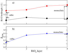
The charge redistribution at the Bi-terminated surfaces is present even in the unrelaxed systems, which turn metallic just by bond breaking (See Supplementary material for unrelaxed cases). When the slabs are allowed to relax, the breathing distortions are washed out at the surface and subsurface Bi planes, contributing to an enhancement of the surface metallicity. In the deeper layers, compressed and expanded octahedra remain without significant changes preserving, there, the insulating charge ordering as in the bulk. In Fig. 4 we plot the average Bi-O bond length (a) and the difference of the ”Atoms in Molecules”(AIM) chargesAIM of the Bi3+ and Bi5+ ions, (b), at each layer for the 13 layers slab obtained with GGA. We observe that both quantities evolve from a monoclinic like situation, in the core of the slab, to a cubic like one in the surface. There is experimental evidence from thin film measurements supporting these resultsGuyot et al. (1993).
We can draw a parallelism between the effect of the surface on the structural and electronic properties of the Bi-terminated film and the effect of temperature on the same properties in bulk BaBiO3. That is, we could think of having ”cold” insulating monoclinic regions in the deeper planes and ”hot” metallic cubic ones close to the surface. We can also make an analogy with the high-Tc superconductor, the doped BaBiO3 in bulk, which turns cubic and metallic upon doping with K or Pb. In this context, the predicted 2DEG at the BiO2 surface deserves further investigation regarding its superconducting properties.
Another interesting finding with potential technological applications is the fact that the BaO surface is insulating. The possibility of drawing BiO2 nanocircuits on top of BaO terminated BaBiO3 surfaces constitutes a subject appealing for exploration. Finally, this surface metallization phenomenon might be present in many other charge ordered materiales. Potential candidates deserving further investigation are CaFeO3V. E. Alexandrov et al (2008), Pb2O3Harrison (2006), LuNiO3I. I. Mazin et al (2007).
Summarizing, in this work we propose a new physical mechanism to generate a two-dimensional electron gas at the surface of charge ordered insulators. It is based on the charge order breaking of the disproportionated ions at these surfaces. In particular, we study the case of BaBiO3(001) by means of first-principles calculations and predict the formation of a 2DEG for Bi- termination. The obtained metallic state is confined to the outer layers and presents a quite high 2D carrier density, of the order of 0.6 electrons per 2D unit cell. This phenomenon is probably not exclusive of BaBiO3 and might occur in other charge ordered semiconductors. It is independent of any external factor such as the ambient oxygen pressure or polar discontinuities, making this system a self-doping surface with promising potential applications to oxide electronics.
The authors thank A. Santander-Syro and M. Rozenberg for suggesting us the problem hereby studied. We also thank both of them and R. Weht for illuminating discussions. The calculations were performed using the ISAAC cluster at the computer center of DCAP-GTIC, CAC-CNEA. This work received financial support through PICT-R1776, PIP-0258, and UBACyT-X123.
References
- (1) M. Lannoo and P. Friedel, Atomic and electronic structure of surfaces. Theoretical foundations (Springer Verlag, Berlin Heidelberg, 1991); Zhen Zhang and John T. Yates,Jr, Chem. Rev. 112, 5520 (2012).
- Ohtomo and Hwang (2004) A. Ohtomo and H. Y. Hwang, Nature 427, 423 (2004).
- N. Reyren et al (2007) N. Reyren et al, Science 317, 1196 (2007).
- A. Brinkman et al. (2007) A. Brinkman et al., Nature Materials 6, 493 (2007).
- Pentcheva and Pickett (2007) R. Pentcheva and W. E. Pickett, Phys. Rev. Lett. 99, 016802 (2007).
- A. Kalabukhov et al. (2007) A. Kalabukhov et al., Phys. Rev. B 75, 121404 (2007).
- G. Herranz et al. (2007) G. Herranz et al., Phys. Rev. Lett. 98, 216803 (2007).
- M. Basletic and et al. (2008) M. Basletic and et al., Nature Materials 7, 621 (2008).
- A. F. Santander-Syro at al. (2011) A. F. Santander-Syro at al., Nature 469, 189 (2011).
- Hohenberg and Kohn (1964) P. Hohenberg and W. Kohn, Phys. Rev. 136, B864 (1964).
- Cox and Sleight (1976) D. Cox and A. Sleight, Solid State Commun. 19, 969 (1976).
- A. W. Sleight et al. (1975) A. W. Sleight et al., Solid State Commun. 17, 27 (1975).
- R. J. Cava et al (1988) R. J. Cava et al, Nature 332, 814 (1988).
- (14) L. F. Mattheiss and D. R. Hamann, Phys. Rev. B 28, 4227 (1983); L. F. Mattheiss and D. R. Hamann, Phys. Rev. Lett. 60, 2681 (1988)r.;
- (15) A. I. Liechtenstein and et al., Phys. Rev. B 44, 5388 (1991); K. Kunc and et al., Solid State Commun. 80, 325 (1991); V. Meregalli and S. Y. Savrasov, Phys. Rev. B 57, 14453 (1998).
- Thonhauser and Rabe (2006) T. Thonhauser and K. M. Rabe, Phys. Rev. B 73, 212106 (2006).
- Perdew and Zunger (1981) J. P. Perdew and A. Zunger, Phys. Rev. B 23, 5048 (1981).
- J. P. Perdew et al. (1996) J. P. Perdew et al., Phys. Rev. Lett. 77, 3865 (1996).
- Not (a) See Ref. C. Franchini et al., 2010 and references there in.
- C. Franchini et al. (2010) C. Franchini et al., Phys. Rev. B 81, 085213 (2010).
- Tran and Blaha (2009) F. Tran and P. Blaha, Phys. Rev. Lett. 102, 226401 (2009). Jochen Heyd1, Gustavo E. Scuseria1, and Matthias Ernzerhof2
- J. et al. (2003) J. Heyd, G. Scuseria, and M. Ernzerhof, J. Chem. Phys. 118, 8207 (2003); A. V. Krukau et al., J. Chem. Phys. 125, 224106 (2006).
- P. Blaha et al. (2002) P. Blaha et al., WIEN2k, An augmented Plane Wave + Local Orbitals Program for Calculating Crystal Properties (Techn. Univ. Wien, Austria, SBN 3-9501031-1-2., 2002).
- Kresse and Furthmüller (1996) G. Kresse and J. Furthmüller, Comput. Matr. Sci. 6, 15 (1996)R; J. Paier et al., J. Chem. Phys. 122, 234102 (2005).
- Not (a) In this work, we study the stoichiometric surface. A deeper analysis of the effect of oxygen vacancies is in general necessary for oxide perovskites. However, simple arguments as the ones described above (Fig. 3 ) can be used to anticipate the robustness of the proposed mechanism in the presence of oxygen vacancies.
- (26) R. F. W. Bader, Atoms in Molecules - A quantum theory (Oxford University Press, New York,1990).
- Guyot et al. (1993) H. Guyot, C. Filippini, and J. Marcus, Journal of Alloys and Compounds 195, 543 (1993), ISSN 0925-8388.
- V. E. Alexandrov et al (2008) V. E. Alexandrov et al, J. Chem. Phys. 129, 214704 (2008).
- Harrison (2006) W. A. Harrison, Phys. Rev. B 74, 245128 (2006).
- I. I. Mazin et al (2007) I. I. Mazin et al, Phys. Rev. Lett. 98, 176406 (2007).