Electron and hole transmission through superconductor - normal metal interfaces
Abstract
We have investigated the transmission of electrons and holes through interfaces between superconducting aluminum (K) and various normal non-magnetic metals (copper, gold, palladium, platinum, and silver) using Andreev-reflection spectroscopy at K. We analysed the point contacts with the modified BTK theory that includes Dynes’ lifetime as a fitting parameter in addition to superconducting energy gap and normal reflection described by . For contact areas from nm2 to nm2 the BTK parameter was 0.5, corresponding to transmission coefficients of about , independent of the normal metal. The very small variation of indicates that the interfaces have a negligible dielectric tunneling barrier. Fermi surface mismatch does not account for the observed transmission coefficient.
pacs:
85.30.Hi, 73.40.-c, 74.45.+cI Introduction
An interface between two conductors presents an obstacle for charge (electron or hole) transport, transmitting a fraction of the incident current and reflecting the remainder . Normal reflection plays a central role in Andreev-reflection spectroscopy according to the BTK theory Blonder1982 which assumes that the transmitted electrons and the retro-reflected holes are affected in the same way. This allows to measure the transmission coefficient of normal-superconductor interfaces. Blonder and Tinkham Blonder1983 explained the usually observed Andreev reflection double-minimum structure - an enhanced resistance around zero bias inside the energy gap - as being due to a combination of tunneling through a dielectric layer and the mismatch of Fermi velocities. A dielectric oxide Simmons1964 or water/ice layer Repphun1995 has to be expected when the contact between the two conductors is not prepared at ultrahigh-vacuum conditions. Even a contact between two identical metals disrupts the crystal lattice symmetry and should lead to some amount of normal reflection. Describing the real interface with a -function barrier and in the one-dimensional free electron approximation Landau1977 , the transmission coefficient can be obtained from Blonder1983
| (1) |
where is the ratio of Fermi velocities and of the two electrodes. Thus one could directly measure Fermi-velocity ratios once the contribution of the dielectric barrier is known.
This seemingly simple situation changed dramatically with the discovery of heavy-fermion superconductors where the ’heavy’ conduction electrons form the Cooper pairs Steglich1979 . The first point-contact study of those compounds by U. Poppe Poppe1985 and Steglich et al. Steglich1985 focussed on Giaever-type tunneling to measure the density of states of the new superconductors and the Josephson effect to probe the symmetry of the heavy-fermion order parameter, without considering Andreev reflection. E. W. Fenton Fenton1985 predicted a huge normal reflection coefficient of interfaces between a heavy-fermion and a conventional metal, corresponding to , because of their very small Fermi velocities down to of that of conventional metals. This idea got partial support by a large background residual resistance of those heavy-fermion contacts where the cross-sectional area could be determined independently Gloos1995 ; Gloos1996a ; Gloos1996b . However, the corresponding tunneling-like Andreev reflection anomalies have never been found.
A second approach by Deutscher and Nozières Deutscher1994 seemed to resolve the question of the puzzlingly small normal reflection. According to them not the heavy particles cross the interface, but the bare ones. This suggests that it is not the mismatch of Fermi velocities but that of the Fermi wave numbers that matters for normal reflection. Equation 1 remains with the ratio of Fermi wave numbers. For interfaces between heavy-fermion compounds and conventional metals this ratio is of order unity, and therefore the parameter should be rather small. Since then many point-contact Andreev reflection experiments on heavy-fermion superconductors have been performed, for example DeWilde1994 ; Park2008 , focussing on the symmetry of the superconducting order parameter, and paying less attention to normal reflection.
Meanwhile, the study of the proximity effect at superconducting - normal metal thin film layered structures, which depends strongly on the transparency of the interfaces, has progressed Attanasio2006 ; Kushnir2009 . Such thin films are usually fabricated in ultra-high vacuum, making a dielectric interface barrier unlikely and leaving Fermi surface mismatch to explain normal reflection. These experiments suggest that (corresponding to ) for contacts between simple metals, considerably less than the expected () in free-electron approximation. One can also measure directly the current perpendicular to plane (CPP) resistance of an interface with a well defined geometry Pratt2009 ; Sharma2009 and compare it with electronic-structure calculations Xu2006 ; Xu2006b . The CPP resistance should contain information about normal reflection, but for us it is difficult to extract.
Measuring spin polarization using Andreev-reflection spectroscopy Soulen1998 is another research topic that relies heavily on normal reflection. According to the general point of view Bugoslavsky2005 ; Baltz2009 , the true spin polarization is only obtained at highly transparent interfaces when while the measured polarization drops to zero around for contacts with conventional ferromagnets like cobalt, iron, and nickel. This strong dependence of the polarisation does not match the results of the Tedrow-Meservey tunneling experiments Tedrow1973 carried out in the opposite limit, indicating that the interface transparency affects the measured polarization Kant2002 ; Woods2004 .
Although the BTK is assumed to be well understood, it is very often treated as a simple fit parameter without further consideration. We show here for contacts between aluminium, one of the most simple superconductors, and various non-magnetic normal metals, that the parameter is very likely not related to Fermi surface mismatch as it is understood today.
II Experimental
Our point contacts were made using the shear (crossed wire) method by gently touching with one sample wire another one. The wires had diameters of either mm (all normal metals) or mm (Al). The contacts were measured at temperatures down to 0.1 K in the vacuum region of a dilution refrigerator. A DC current with a small superposed AC component is injected into the contact and the voltage drop across the contact measured to obtain the characteristics as well as the differential resistance spectrum . We estimate the contact radius by the ballistic Sharvin resistance where . In free-electron approximation these metals have typically Fermi wave numbers of nm-1 Ashcroft1976 . Thus a contact has a radius of nm, assuming circular symmetry, or cross-sectional area. This agrees reasonably well with the fm2 CPP resistance of Al - Cu interfaces Sharma2009 .
We have chosen only contacts that had spectra with the characteristic double-minimum structure of Andreev reflection like the ones in Figures 1 and 2, roughly half of all contacts. The spectra were analysed using the modified BTK theory that includes Dynes’ lifetime parameter Plecenik1994 . The normal resistance agreed with the asymptotic differential resistance at large bias voltages. Side peaks at finite bias voltage, for example due to the self-magnetic field, were easy to recognize and did therefore not affect the analysis with respect to normal reflection.
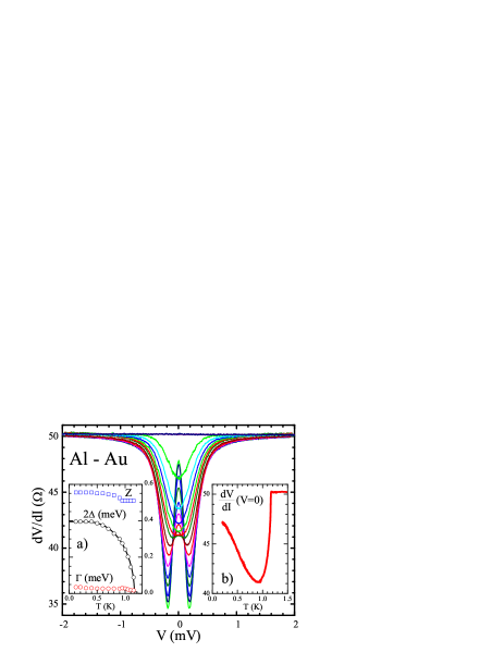
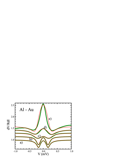
Figure 1 shows the spectra of one of the Al - Au contacts as function of temperature. The extracted energy gap follows closely the BCS temperature dependence, while and remain nearly constant. As long as the double-minimum structure exists, for this contact up to 0.9 K, all three parameters can be determined independently (the error bars are smaller than the symbol sizes). The double minimum collapses into a single one at K. For those spectra we kept constant and fitted only and . The contacts discussed below were measured at K to reduce thermal smearing in order to reliably determine . Figure 2 shows a selection of typical spectra over the accessible resistance range together with fit curves and the extracted parameters. Noticeable deviations from the BTK-type fit appear only at very large resistances, that is very small contacts.
III Results and discussion
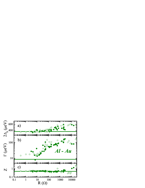
Figure 3 shows the derived parameters , , and as function of normal resistance for contacts between superconducting Al and Au. The energy gap agrees well with the literature value of eV from below up to several . Then the gap increases to about twice its low-resistance value. The lifetime parameter is barely resolvable at contacts with small resistance because of the eV thermal smearing. Between the lifetime parameter increases almost linearly, and saturates at round eV at high resistances.
Most astonishingly, the parameter stays constant at from below up to several , that means from contact areas of more than nm2 to less than nm2. Reflection at a dielectric barrier should result in a strong variation of , depending on how a specific contact is made, because the transmission coefficient depends exponentially on the barrier width and height Simmons1964 . The extremely small variation of thus indicates a negligibly weak dielectric tunneling barrier. This appears plausible for shear contacts because the two electrode wires slide along each other, scratching the surfaces and thereby removing a possible oxide or water/ice layer before the contact is formed. increases only in the k range towards the transition to vacuum tunneling. At such high resistances the contact consists of only a few conduction channels, each with its own reflection coefficient, where the ones with the large are not averaged away. This might also contribute to the deviations from the BTK-type fits in Figure 2.
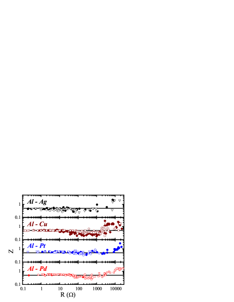
Contacts with the other normal metals Ag, Cu, Pd, and Pt behave similarly as summarized for the parameter in Figure 4. However, there appears to be a softening of especially for the Al - Cu contacts at around , coinciding with the increasing and the saturation of . The suspicion that this partial reduction of results from electrical noise can be discarded because recovers at higher resistances which should be even more susceptible to noise. An alternative explanation for this behaviour might be a real size-dependent property of the contacts, analogue to the Kondo-like zero-bias anomalies Gloos2009 .
As discussed for the Al - Au contacts, the rather constant makes a noticeable dielectric barrier unlikely also for contacts with the other normal metals. This leaves Fermi surface mismatch to explain the finite . The metal combinations presented here should have either in free-electron approximation or based on proximity-effect estimates mentioned above. Our experimental data fit neither of those two limits. In addition, the argument that excludes tunneling also holds for Fermi surface mismatch because we can not control how the crystallites that actually form the contact are oriented. Can it be that Fermi surface mismatch does not contribute to normal reflection as measured by Andreev reflection?
Electrons as well as Andreev-reflected holes cross a real dielectric tunneling barrier with a certain probability, while the remainder is normally reflected. This allows to extract the transmission or the reflection coefficient from a single Andreev-reflection spectrum. Normal reflection due to Fermi surface mismatch works differently: a certain kind of the incident electrons - those with the wrong wave number and direction of incidence - can not cross the interface. Since only electrons that have been transmitted can be Andreev-reflected, the retro-reflected holes have already the right properties to be transmitted back through the interface. If this is correct then Fermi surface mismatch can not be resolved using Andreev-reflection spectroscopy.
IV Conclusion
We have found that the BTK parameter of interfaces with superconducting Al does neither depend sensitively on the size of the contacts nor on the normal metal. Its tiny variation over a vast range of contact areas has lead us to conclude the absence of a dielectric tunneling barrier. The same argument holds for Fermi surface mismatch because of the uncontrollable orientation of the crystallites that form the contact. Moreover, the average experimental disagrees with the free-electron prediction () and with the results of the proximity studies (). The experiments on reflection at or transmission through normal-superconducting interfaces and their interpretation remind us that different methods can yield different results for the same physical property. In the end we are left with a new – but at the same time old – mystery of the origin of the Andreev reflection double minimum anomaly described by .
Acknowledgements.
E. T. acknowledges a two-year grant from the Graduate School of Materials Research (GSMR), 20014 Turku, Finland. We thank the Jenny and Antti Wihuri Foundation for financial support.References
- (1) G. E. Blonder, M. Tinkham, and T. M. Klapwijk, Phys. Rev. B 25, 4515 (1982).
- (2) G. E. Blonder and M. Tinkham, Phys. Rev. B 27, 112 (1983).
- (3) J. G. Simmons, J. Appl. Phys. 35, 2655 (1964).
- (4) G. Repphun and J. Halbritter, J. Vac. Sci. Technol. A 13, 1693 ()1995).
- (5) L. D. Landau and E. M. Lifshitz, Course of Theoretical Physics Volume 3. Quantum Mechanics (3rd Edition, Pergamon Press, Oxford 1977) pp. 60.
- (6) F. Steglich, J. Aarts, C. D. Bredl, W. Lieke, D. Meschede, W. Franz, and H. Schäfer, Phys. Rev. Lett. 43, 1892 (1979).
- (7) U. Poppe, J. Magn. Magn. Materials 52, 157 (1985).
- (8) F. Steglich, U. Rauchschwalbe, U. Gottwick, H. M. Mayer, G. Sparn, N. Grewe, U. Poppe, J. J. M. Franse, J. Appl. Phys. 57, 3054 (1985).
- (9) E. W. Fenton, Solid State Commun. 54, 709 (1985).
- (10) K. Gloos, F. Martin, C. Schank, C. Geibel, and F. Steglich, Physica B: Condensed Matter 206-207, 282 (1995).
- (11) K. Gloos, C. Geibel, R. Müller-Reisener, and C. Schank, Physica B: Condensed Matter 218, 169 (1996).
- (12) K. Gloos, F. B. Anders, B. Buschinger, C. Geibel, K. Heuser, F. Jährling, J. S. Kim, R. Klemens, R. Müller-Reisener, C. Schank, and G. R. Stewart, J. Low Temp. Phys. 105, 37 (1996).
- (13) G. Deutscher and P. Nozières, Phys. Rev. B 50,13557 (1994).
- (14) Y. De Wilde, J. Heil, A. G. M. Jansen, P. Wyder, R. Deltour, W. Assmus, A. Menovsky, W. Sun, and L. Taillefer, Phys. Rev. Lett. 72, 2278 (1994).
- (15) W. K. Park, J. L. Sarrao, J. D. Thompson, and L. H. Greene, Phys. Rev. Lett. 100, 177001 (2008).
- (16) C. Attanasio in: Nanoscale Devices - Fundamentals and Applications, ed R. Gross et al. (Springer, 2006) pp 241.
- (17) V. N. Kushnir, S. L. Prischepa, C. Cirillo, and C. Attanasio, J. Appl. Phys. 106, 113917 (2009).
- (18) W. P. Pratt Jr., and J. Bass, Appl. Surface Science 256, 399 (2009).
- (19) A. Sharma, N. Theodoropoulou, S. Wang, K. Xia, W. P. Pratt, Jr., and J. Bass, J. Appl. Phys. 105, 123920 (2009).
- (20) P. X. Xu, K. Xia, M. Zwierzycki, M. Talanana, and P. J. Kelly, Phys. Rev. Lett. 96, 176602 (2006).
- (21) P. X. Xu and K. Xia, Phys. Rev. B 74, 184026 (2006).
- (22) R. J. Soulen Jr., J. M. Byers, M. S. Osofsky, B. Nadgorny, T. Ambrose, S. F. Cheng, P. R. Broussard, C. T. Tanaka, J. Nowack, J. S. Moodera, A. Barry, and J. M. D. Coey, Science 282 85 (1998).
- (23) Y. Bugoslavsky, Y. Miyoshi, S. K. Clowes, W. R. Branford, M. Lake, I. Brown, A. D. Caplin, and L. F. Cohen, Phys. Rev. B 71, 104523 (2005).
- (24) V. Baltz, A. D. Naylor, K. M. Seemann, W. Elder, S. Sheen, K. Westerholt, H. Zabel, G. Burnell, C. H. Marrows, and B. J. Hickey, J. Phys.: Condens. Matter 21, 095701 (2009).
- (25) P. M. Tedrow and R. Meservey, Phys. Rev. B 7, 318 (1973).
- (26) C. H. Kant, O. Kurnosikov, A. T. Filip, P. LeClair, H. J. M. Swagten, and W. J. M. de Jonge, Phys. Rev. B 66, 212403 (2002).
- (27) G. T. Woods, J. Soulen, Jr., I. Mazin, B. Nadgorny, M. S. Osofsky, J. Sanders, H. Srikanth, W. F. Egelhoff, and R. Datla, Phys. Rev. B 70, 054416 (2004).
- (28) N. W. Ashcroft and N. D. Mermin, Solid State Physics (Thomson Learning, 1976) p. 38.
- (29) A. Pleceník, M. Grajcar, and S̆. Ben̆ac̆ka, P. Seidel, and A. Pfuch, Phys. Rev. B 49, 10016 (1994).
- (30) K. Gloos, Low Temp. Phys. 35, 935 (2009) [Fiz. Nizk. Temp. Phys. 35, 1204 (2009)].