Excitation of confined modes on particle arrays
Abstract
We describe both theoretically and experimentally the existence and excitation of confined modes in planar arrays of gold nanodisks. Ordered 2D lattices of monodispersive nanoparticles are manufactured, embedded in a silica matrix, and exposed to evanescent prism-coupling illumination, leading to dark features in the reflectivity, which signal the presence of confined modes guided along the arrays. We find remarkable agreement between theory and experiment in the frequency-momentum dispersion of the resonances. Direct excitation of these modes reveals long propagation distances and deep extinction features. This characterization of guided modes shows the great potential of metallic particle arrays for optical signal processing and distant sensing applications.
Metal nanoparticles are capable of producing high levels of confinement and enhancement of incident light LSB03 . These appealing properties make them useful for sensing (e.g., through detection of plasmon-resonance shifts MV03 ; DTH06 ; KE06 ; SAT08 ; AHL08 and surface-enhanced Raman scattering NE97 ; KWK97 ; JXK05 ; TJO05 ; paper125 ), cancer therapy QPA08 ; HSB03 , drug delivery LSH11 , improved photovoltaics CP08 ; AP10 , and catalysis AMO01 ; K02 . These applications have attracted a considerable degree of interest on the optical properties of nanoparticles, which strongly depend on size, morphology, and composition MBS02 ; KCZ03 ; paper112 . The interaction between neighboring particles can also produce changes in their optical behavior, which are dramatic when small particle gaps are involved B1982 ; NOP04 ; paper075 . Additionally, long-range interactions lead to collective modes in ordered paper142 ; KHH10 and disordered OER11 particle arrangements, which have been proposed for waveguiding in both 1D QLK98 ; MKA03 and 2D paper105 ; paper142 configurations.
In particular, lattice resonances in 2D ordered particle arrays act as an effective way of creating guided modes paper090 that are strongly dependent on the choice of materials, particle size and shape, and lattice parameters, leading to distinct TE and TM modes paper142 ; RSB12 . This configures a versatile platform for applications to distant sensing and waveguiding, which deserve a detailed characterization of the arrays. Direct far-field sampling of quasi-bounded modes in 2D arrays through diffracted orders have been extensively reported AB08 ; KSG08 ; CSY08 ; VGG09-2 ; VGG09 ; ZO11 . Additionally, theoretical descriptions are available paper164 , which become particularly intuitive when assuming dipole inter-particle interactions paper090 ; paper142 . However, guided modes in metal particle arrays have not been yet directly sampled (i.e., sampled without the assistance of diffraction to couple to far-field radiation), and a detailed experimental study of their optical behavior is still missing.
In this Letter, we report direct observation of guided modes in ordered gold-particle arrays through dips in their evanescent-field reflection using the Otto configuration O1967 ; NH06 . Gold nanodisks have been fabricated by imprint lithography VS07 and embedded in a symmetric silica environment [Fig. 1(a,b)]. A high-index prism is then used for evanescent coupling of incident light [Fig. 1(c)]. The reflected signal unambiguously shows the presence of guided modes. We further report electromagnetic simulations for both the guided-mode dispersion relations and the reflectivity under prism illumination. Experiment and theory are in excellent agreement for the dispersion relations and the mode propagation distances. Our results bear some resemblance to guided modes in photonic crystal waveguides JVF97 ; LCH98 ; JFV99 and electromagnetic surface waves in drilled metal films UT1973 .
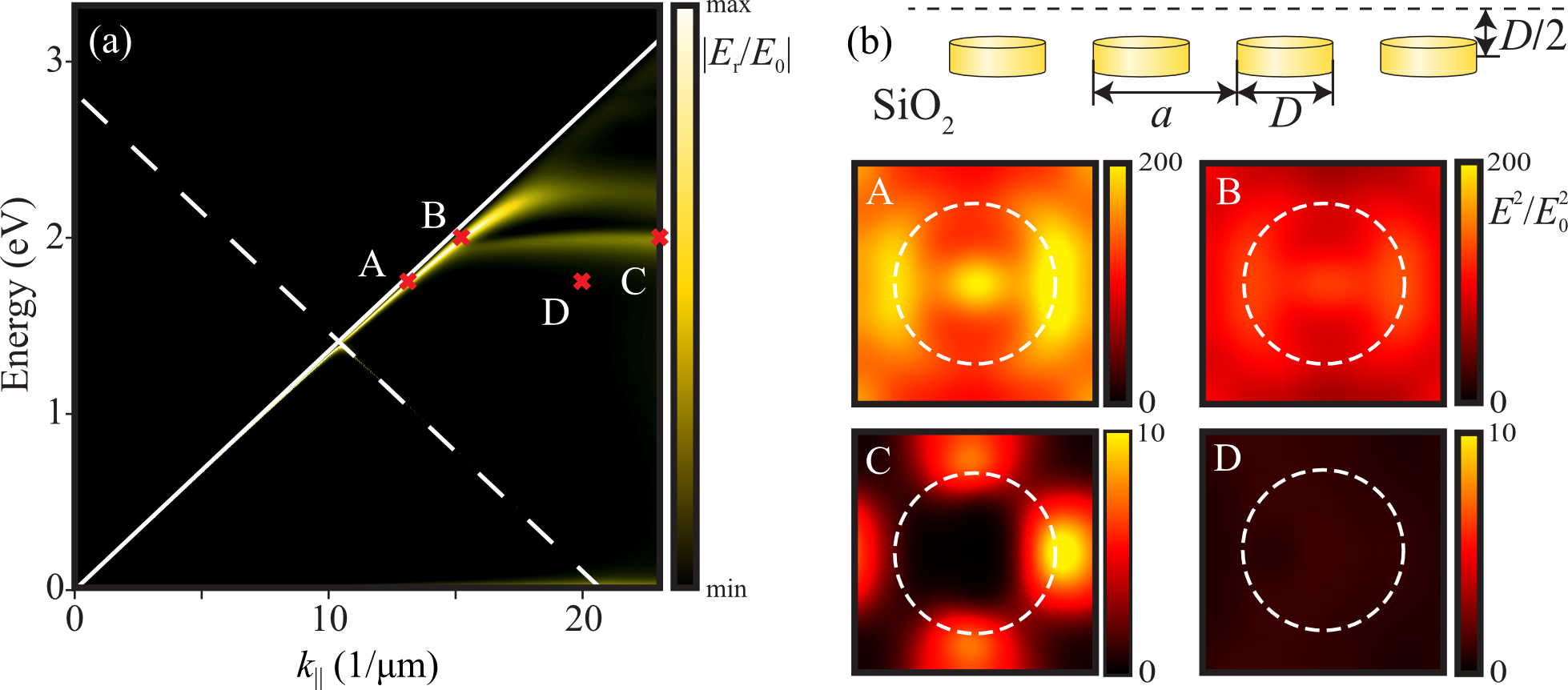
The array modes under study originate in the lattice resonances produced by long-range interaction between the particles close to the onset of different diffraction orders paper142 . Under such conditions, there is constructive interference of the fields scattered by the particles, leading to array-confined modes, which are in fact guided modes that propagate along the plane of the array. These modes show up at frequencies to the red with respect to the light line in a frequency-wavevector diagram paper090 . In Fig. 2(a) we show the calculated reflection coefficient of arrays of gold nanodisks placed in a symmetric SiO2 environment. The dispersion diagram is dominated by two types of features: a prominent one arising from the noted lattice resonances; and a weaker one associated with the excitation of localized surface plasmons that are confined at the gaps between neighboring nanoparticles NOP04 (see below). The reflection coefficient is peaked along a line close to the light cone (solid line), indicating the position of the dispersion relation of the lattice modes. For reference, we also show in the diagram the umklapp folding of the light cone (dashed line), which crosses the light cone at the boundary of the first Brillouin zone (BZ). While the lattice resonance within the first BZ is both too narrow and close to the light line to be resolved in the figure, it is clearly visible withing the second BZ.
The intensity of the electric field, which is represented in Fig. 2(b) for a unit cell at a distance from the middle plane of the lattice, clearly shows the collective character of the resonance. Along the dispersion relation of the propagating mode, such at positions A and B, we have large values of the field enhancement spreading all over the plane, with relatively small spatial variations. We also represent the field at the weaker, relatively flat spectral feature below the resonance at point C. Clearly, the latter shows strong localization at the particle gaps, which is consistent with an interpretation in terms of localized gap plasmons between neighboring nanoparticles and explains the observed vanishing group velocity. Under non-resonant incidence conditions (i.e., away from the propagating mode and localized plasmon regions), the enhancement is featureless and weak, as shown for point D.
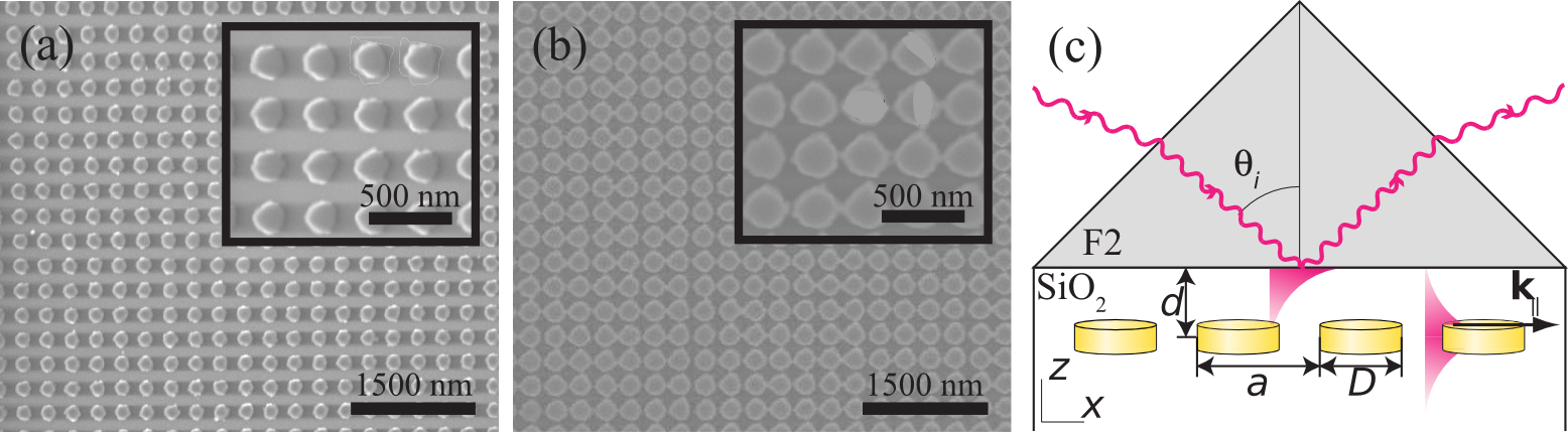
Arrays embedded in a symmetric environment thus display sharp resonances that can be easily modeled theoretically, but their fabrication and characterization is difficult compared to arrays supported on a substrate. A high degree of asymmetry is known to strongly modify and even prevent the existence of the lattice resonances paper142 ; paper164 . In order to reach a compromise between these two extreme situations, we have fabricated gold nanodisk arrays on a SiO2 substrate and added a dielectric capping of the same material (1(a)). This capping of thickness nm not only ensures the existence of the resonant modes, but also provides protection for the nanostructure in potential device applications. We have measured the reflectivity spectra of these samples in a rotation stage using a coupling prism of F2 glass. When light is reflected at the prism-sample interface under total-internal reflection conditions, it produces an evanescent field that,for values of the parallel momentum matching those of the guided modes, is coupled into the latter. This coupling transfers energy that is dissipated due to losses in the metallic nanoparticles, therefore producing a dip in the reflection spectrum, which is a signature of the excitation of a surface mode O1967 .
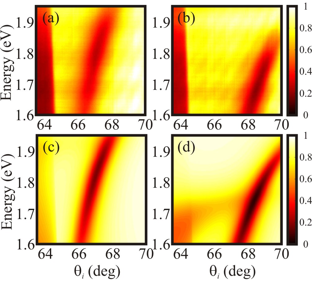
The spectral dependence of this dip can be clearly resolved in Fig. 3, where it shows up to the right of the critical angle (). The agreement between theory [Fig. 3(c,d)] and experiment [Fig. 3(a,b)] is excellent in position, intensity, and width of the spectral features for samples with two different particle diameters [nm in Fig. 3(a,c) and nm in Fig. 3(b,d)]. Some discrepancies are observed in the features at the left end of the angular region under investigation, which we attribute to systematic errors in the characterization setup, which is optimized for data collection to the right of the critical angle. As expected from the calculations of Fig. 2 for a symmetric environment, the resonance appears close to the light line and nearly parallel to it, specially for the smallest particles. Incidentally, almost perfect coupling takes place, with the reflectance reaching values close to zero.
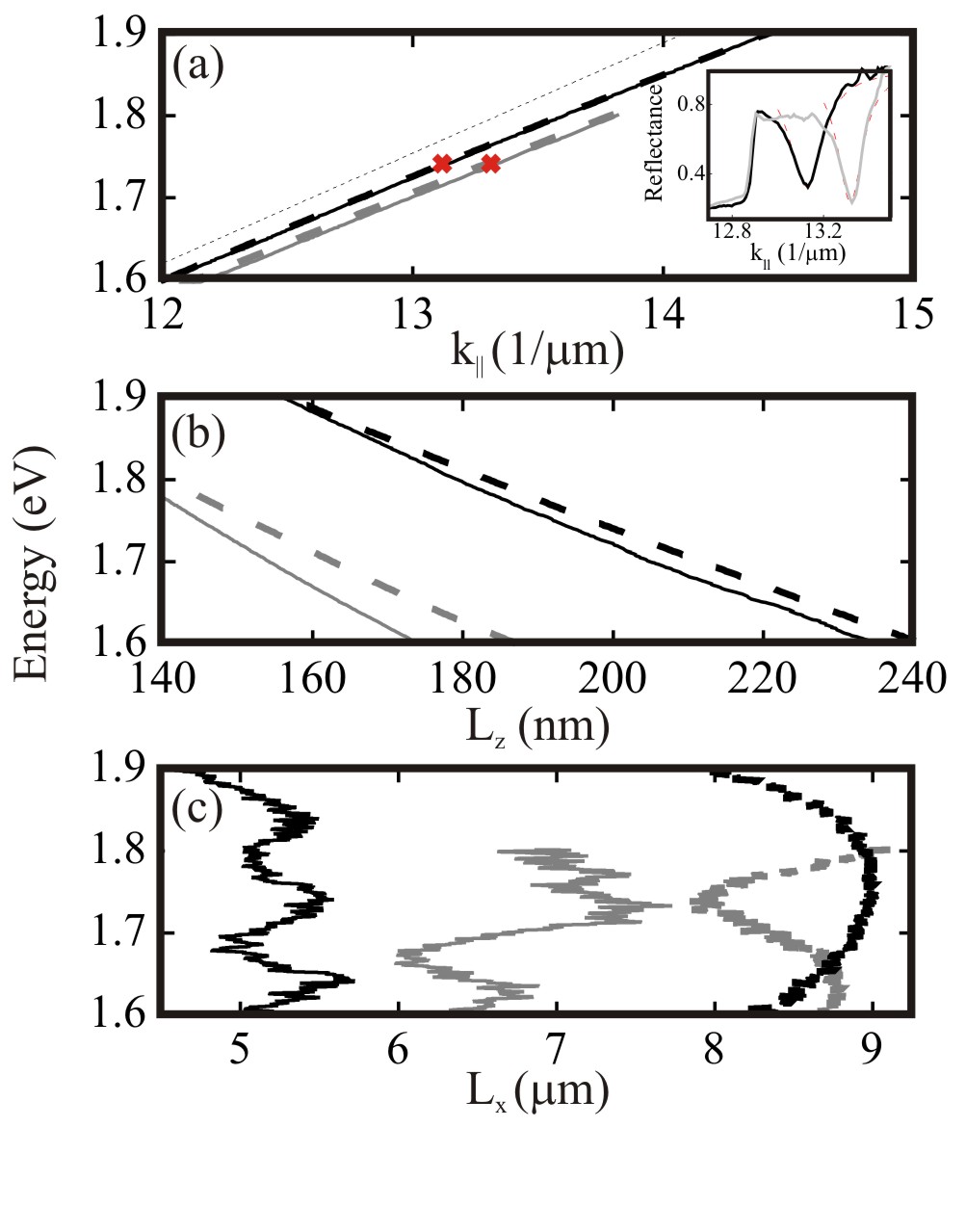
A more detailed characterization of the modes is presented in Fig. 4. Panel (a) shows excellent agreement between the theoretical (dashed curves) and experimental (solid curves) dispersion relations for both particle sizes. The degree of confinement, indicated by the separation from the light (dotted) line in Fig. 4(a) and also by the penetration of the field intensity outside the array in Fig. 4(b), is also in excellent agreement. Notice that this penetration distanceVGG09 is comparable to the separation of 600 nm between the prism and the particles, but the modes are still well defined and clearly resolvable.
Finally, we have calculated the propagation distance along the plane of the array [Fig. 4(c)] by fitting the reflectance dips to Lorentzians [see insets in Fig. 4(a)]. Theory predicts larger propagation than what is observed in the experiment, and we attribute this discrepancy to imperfections in the shape and position of the particles. Actually, the discrepancy between theory and experiment is less pronounced for the largest particles under consideration (gray curves), for which variations in morphology with the same degree of absolute tolerance are relatively smaller. Propagation distances of a few microns ( surface-mode wavelengths) are obtained.
In conclusion, we have experimentally demonstrated the existence of confined propagating modes in planar arrays of plasmonic nanoparticles, and we have determined their dispersion relation and characteristic lengths. Our electromagnetic simulations are in excellent agreement with the experiments. These results should trigger further research into the direct spatial mapping of guided modes. Our particle arrays can be potentially used to propagate optical signals. They can also assist distant sensing, whereby the optical signal from the object or substance to be sensed propagates through an array to the position at which the detector is placed. This possibility provides a natural hybrid between plasmon-based sensors and nanoparticle-based waveguiding.
This work has been supported in part by the European Union (NMP4-2006-016881-SPANS, NMP4-SL-2008-213669-ENSEMBLE, FP7-ICT-2009-4-248909-LIMA, and FP7-ICT-2009-4-248855-N4E), the Spanish MEC (MAT2010-14885 and Consolider Nano-Light.es), and the research program of the Foundation for Fundamental Research on Matter (FOM), which is financially supported by the Netherlands Organization for Fundamental Research (NWO) and is part of an industrial partnership program between Philips and FOM. It is also supported in part by NanoNextNL, a micro and nanotechnology consortium of the Government of the Netherlands and 130 partners. X.M.B. acknowledges a Spanish CSIC-JAE grant.
References
- (1) K. R. Li, M. I. Stockman, and D. J. Bergman, “Self-similar chain of metal nanospheres as an efficient nanolens,” Phys. Rev. Lett. 91, 227402 (2003).
- (2) A. McFarland and R. Van Duyne, “Single silver nanoparticles as real-time optical sensors with zeptomole sensitivity,” Nano Lett. 3, 1057–1062 (2003).
- (3) A. B. Dahlin, J. O. Tegenfeldt, and F. Höök, “Improving the instrumental resolution of sensors based on localized surface plasmon resonance,” An. Chem. 78, 4416–4423 (2006).
- (4) K.-S. Lee and M. A. El-Sayed, “Gold and silver nanoparticles in sensing and imaging: Sensitivity of plasmon response to size, shape, and metal composition,” J. Phys. Chem. B 110, 19220–19225 (2006).
- (5) M. E. Stewart, C. R. Anderton, L. B. Thompson, J. Maria, S. K. Gray, J. A. Rogers, and R. G. Nuzzo, “Nanostructured plasmonic sensors,” Chem. Rev. 108, 494–521 (2008).
- (6) J. N. Anker, W. P. Hall, O. Lyandres, N. C. Shah, J. Zhao, and R. P. Van Duyne, “Biosensing with plasmonic nanosensors,” Nat. Mater. 7, 442–453 (2008).
- (7) S. Nie and S. R. Emory, “Probing single molecules and single nanoparticles by surface-enhanced raman scattering,” Science 275, 1102–1106 (1997).
- (8) K. Kneipp, Y. Wang, H. Kneipp, L. T. Perelman, I. Itzkan, R. R. Dasari, and M. S. Feld, “Single molecule detection using surface-enhanced Raman scattering (SERS),” Phys. Rev. Lett. 78, 1667–1670 (1997).
- (9) P. Johansson, H. Xu, and M. Käll, “Surface-enhanced raman scattering and fluorescence near metal nanoparticles,” Phys. Rev. B 72, 035427 (2005).
- (10) C. E. Talley, J. B. Jackson, C. Oubre, N. K. Grady, C. W. Hollars, S. M. Lane, T. R. Huser, P. Nordlander, and N. J. Halas, “Surface-enhanced Raman scattering from individual au nanoparticles and nanoparticle dimer substrates,” Nano Lett. 5, 1569–1574 (2005).
- (11) L. Rodríguez-Lorenzo, R. A. Álvarez-Puebla, I. Pastoriza-Santos, S. Mazzucco, O. Stéphan, M. Kociak, L. M. Liz-Marzán, and F. J. García de Abajo, “Zeptomol detection through controlled ultrasensitive surface-enhanced Raman scattering,” J. Am. Chem. Soc. 131, 4616–4618 (2009).
- (12) X. Qian, X. H. Peng, D. O. Ansari, Q. Yin-Goen, G. Z. Chen, D. M. Shin, L. Yang, A. N. Young, M. D. Wang, and S. Nie, “In vivo tumor targeting and spectroscopic detection with surface-enhanced raman nanoparticle tags,” Nat. Biotech. 26, 83–90 (2008).
- (13) L. Hirsch, R. Stafford, J. Bankson, S. Sershen, B. Rivera, R. Price, J. Hazle, N. Halas, and J. West, “Nanoshell-mediated near-infrared thermal therapy of tumors under magnetic resonance guidance,” Proc. Natl. Acad. Sci. 100, 13549–13554 (2003).
- (14) Y. L. Luo, Y. S. Shiao, and Y. F. Huang, “Release of photoactivatable drugs from plasmonic nanoparticles for targeted cancer therapy,” ACS Nano 5, 7796–7804 (2011).
- (15) K. R. Catchpole and A. Polman, “Plasmonic solar cells,” Opt. Express 16, 21793–21800 (2008).
- (16) H. A. Atwater and A. Polman, “Plasmonics for improved photovoltaic devices,” Nat. Mater. 9, 205–213 (2010).
- (17) R. Asahi, T. Morikawa, T. Ohwaki, K. Aoki, and Y. Taga, “Visible-light photocatalysis in nitrogen-doped titanium oxides,” Science 293, 269–271 (2001).
- (18) P. V. Kamat, “Photophysical, photochemical and photocatalytic aspects of metal nanoparticles,” J. Phys. Chem. B 106, 7729–7744 (2002).
- (19) J. J. Mock, M. Barbic, D. R. Smith, D. A. Schultz, , and S. Schultz, “Shape effects in plasmon resonance of individual colloidal silver nanoparticles,” J. Chem. Phys. 116, 6755–6759 (2002).
- (20) K. L. Kelly, E. Coronado, L. L. Zhao, and G. C. Schatz, “The optical properties of metal nanoparticles: The influence of size, shape, and dielectric environment,” J. Phys. Chem. B 107, 668–677 (2003).
- (21) V. Myroshnychenko, J. Rodríguez-Fernández, I. Pastoriza-Santos, A. M. Funston, C. Novo, P. Mulvaney, L. M. Liz-Marzán, and F. J. García de Abajo, “Modelling the optical response of gold nanoparticles,” Chem. Soc. Rev. 37, 1792–1805 (2008).
- (22) P. E. Batson, “A new surface plasmon resonance in clusters of small aluminum spheres,” Ultramicroscopy 9, 277–282 (1982).
- (23) P. Nordlander, C. Oubre, E. Prodan, K. Li, and M. I. Stockman, “Plasmon hybridizaton in nanoparticle dimers,” Nano Lett. 4, 899–903 (2004).
- (24) I. Romero, J. Aizpurua, G. W. Bryant, and F. J. García de Abajo, “Plasmons in nearly touching metallic nanoparticles: Singular response in the limit of touching dimers,” Opt. Express 14, 9988–9999 (2006).
- (25) X. M. Bendaña and F. J. García de Abajo, “Confined collective excitations of self-standing and supported planar periodic particle arrays,” Opt. Express 17, 18826–18835 (2009).
- (26) D. M. Koller, U. Hohenester, A. Hohenau, H. Ditlbacher, F. Reil, N. Galler, F. R. Aussenegg, A. Leitner, A. Trügler, and J. R. Krenn, “Superresolution moire mapping of particle plasmon modes,” Phys. Rev. Lett. 104, 143901 (2010).
- (27) M. A. Otte, M. C. Estevez, D. Regatos, L. M. Lechuga, and B. Sepulveda, “Guiding light in monolayers of sparse and random plasmonic meta-atoms,” ACS NANO 5, 9179–9186 (2011).
- (28) M. Quinten, A. Leitner, J. R. Krenn, and F. R. Aussenegg, “Electromagnetic energy transport via linear chains of silver nanoparticles,” Opt. Lett. 23, 1331–1333 (1998).
- (29) S. A. Maier, P. G. Kik, H. A. Atwater, S. Meltzer, E. Harel, B. E. Koel, and A. A. G. Requicha, “Local detection of electromagnetic energy transport below the diffraction limit in metal nanoparticle plasmon waveguides,” Nat. Mater. 2, 229–232 (2003).
- (30) R. Sainidou and F. J. García de Abajo, “Plasmon guided modes in nanoparticle metamaterials,” Opt. Express 16, 4499–4506 (2008).
- (31) F. J. García de Abajo, “Colloquium: Light scattering by particle and hole arrays,” Rev. Mod. Phys. 79, 1267–1290 (2007).
- (32) S. R. K. Rodríguez, M. C. Schaafsma, A. Berrier, and J. Gomez-Rivas, “Collective resonances in plasmonic crystals: Size matters,” Phys. B p. DOI: 10.1016/j.physb.2012.03.053 (2012).
- (33) B. Auguié and W. L. Barnes, “Collective resonances in gold nanoparticle arrays,” Phys. Rev. Lett. 101, 143902 (2008).
- (34) V. G. Kravets, F. Schedin, and A. N. Grigorenko, “Extremely narrow plasmon resonances based on diffraction coupling of localized plasmons in arrays of metallic nanoparticles,” Phys. Rev. Lett. 101, 087403 (2008).
- (35) Y. Chu, E. Schonbrun, T. Yang, and K. B. Crozier, “Experimental observation of narrow surface plasmon resonances in gold nanoparticle arrays,” Appl. Phys. Lett. 93, 181108 (2008).
- (36) G. Vecchi, V. Giannini, and J. Gómez Rivas, “Shaping the fluorescent emission by lattice resonances in plasmonic crystals of nanoantennas,” Phys. Rev. Lett. 102, 146807 (2009).
- (37) G. Vecchi, V. Giannini, and J. Gómez Rivas, “Surface modes in plasmonic crystals induced by diffractive coupling of nanoantennas,” Phys. Rev. B 80, 201401 (2009).
- (38) W. Zhou and T. W. Odom, “Tunable subradiant lattice plasmons by out-of-plane dipolar interactions,” Nat. Nanotech. 6, 423–427 (2011).
- (39) B. Auguié, X. M. Bendaña, W. L. Barnes, and F. J. García de Abajo, “Diffractive arrays of gold nanoparticles near an interface: Critical role of the substrate,” Phys. Rev. B 82, 155447 (2010).
- (40) A. Otto, “Theory of plasmon excitation in thin films by electrons of non-normal incidence,” Phys. Status Solidi 22, 401–406 (1967).
- (41) L. Novotny and B. Hecht, Principles of Nano-Optics (Cambridge University Press, New York, 2006).
- (42) M. A. Verschuuren and H. A. van Sprang, “3d photonic structuresby sol-gel imprint lithography.” Mater. Res. Soc. Symp. Proc. 1002, 1002‐N03‐05 (2007).
- (43) J. D. Joannopoulos, P. R. Villeneuve, and S. H. Fan, “Photonic crystals: Putting a new twist on light,” Nature 386, 143–149 (1997).
- (44) S. Y. Lin, E. Chow, V. Hietala, P. R. Villeneuve, and J. D. Joannopoulos, “Experimental demonstration of guiding and bending of electromagnetic waves in a photonic crystal,” Science 282, 274–276 (1998).
- (45) S. G. Johnson, S. Fan, P. R. Villeneuve, J. D. Joannopoulos, and L. A. Kolodziejski, “Guided modes in photonic crystal slabs,” Phys. Rev. B 60, 5751–5758 (1999).
- (46) R. Ulrich and M. Tacke, “Submillimeter waveguiding on periodic metal structure,” Appl. Phys. Lett. 22, 251–253 (1973).