E-mail: yuri.evangelista@iaps.inaf.it, Telephone: +39 06 4993 4657
Simulations of the X-ray imaging capabilities of the Silicon Drift Detectors (SDD) for the LOFT Wide Field Monitor
Abstract
The Large Observatory For X-ray Timing (LOFT), selected by ESA as one of the four Cosmic Vision M3 candidate missions to undergo an assessment phase, will revolutionize the study of compact objects in our galaxy and of the brightest supermassive black holes in active galactic nuclei. The Large Area Detector (LAD), carrying an unprecedented effective area of 10 m2, is complemented by a coded-mask Wide Field Monitor, in charge of monitoring a large fraction of the sky potentially accessible to the LAD, to provide the history and context for the sources observed by LAD and to trigger its observations on their most interesting and extreme states. In this paper we present detailed simulations of the imaging capabilities of the Silicon Drift Detectors developed for the LOFT Wide Field Monitor detection plane. The simulations explore a large parameter space for both the detector design and the environmental conditions, allowing us to optimize the detector characteristics and demonstrating the X-ray imaging performance of the large-area SDDs in the 2–50 keV energy band.
keywords:
LOFT Wide Field Monitor, Silicon Drift Detectors, SDD, simulations, spatial resolution1 INTRODUCTION
The LOFT[1] WFM is a coded aperture imaging experiment designed on the heritage of the SuperAGILE experiment [2], successfully operating in orbit since 2007 [3]. With the 120 m position resolution provided by its single-sided Silicon microstrip detector, SuperAGILE demonstrated the feasibility of a compact, large-area, light, low-power and high resolution X-ray imager, with steradian-wide field of view. The LOFT WFM applies the same concept, with improvements provided by the superior performance Silicon Drift Detectors (SDDs) in place of the Si microstrips. These detectors provide a lower energy threshold and better energy resolution with respect to the microstrips, and represent the state-of-the art in large area, monolithic Silicon detectors.
The working principle of the WFM is the classical sky encoding by coded masks[4] and is widely used in space borne instruments (e.g. INTEGRAL, RXTE/ASM, Swift/BAT). The mask shadow recorded by the position-sensitive detector can be deconvolved by using the procedures[5] to recover the image of the sky, with an angular resolution that depends on the mask element pitch, the mask-detector distance and the detector spatial resolution. In this paper we describe the results obtained by means of a Monte Carlo simulator specifically developed to evaluate the spatial resolution capabilities of the large area Silicon Drift Detectors. This tool allowed us to understand and optimize the detector performance by investigating different detector designs (i.e. anode pitch), environmental conditions (detector temperature, radiation damage) and read-out electronics performance.
In the following we will describe the SDD working principle and the charge cloud dynamics inside the Silicon bulk (Section 2), the preliminary imaging results obtained with a 8-channels discrete read-out (Section 3), the structure of the MC simulator developed for the LOFT/WFM (Section 4) and the simulation results (Section 5). Finally, in Section 6, we draw our conclusions.
2 Working principle of the Silicon Drift Detector
As reported above, the proposed technology for the WFM detection plane is represented by an improved version of the large-area Silicon Drift Detectors (SDDs) developed for the Inner Tracking System in the ALICE experiment of the Large Hadron Collider (LHC) at CERN[6, 7], by one of the scientific institutes in the LOFT Consortium — INFN Trieste, Italy — in co-operation with Canberra Inc. The key properties of the Si drift detectors[8] are their capability to read-out a large photon collecting area with a small set of low-capacitance (thus low-noise) anodes and their very small weight (1 kg m-2).
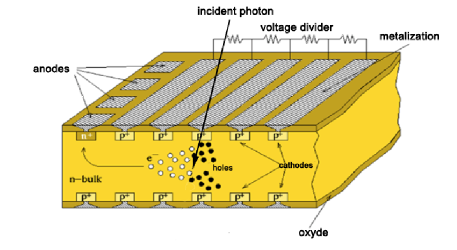
The working principle of the Silicon drift detectors is shown in Figure 1. When a photon is absorbed in the Si bulk it creates a cloud of electron-hole pairs. The holes are collected on the cathodes implanted on both the detector surface while the cloud of electrons is focused in the middle plane of the detector by a parabolic potential distribution. The cloud then drifts towards the read-out anodes by means of a constant electric field sustained by negative voltages applied to the cathodes with progressively reducing amplitude down to the anodes at 0 V. When focused in the detector middle plane, the cloud quickly assumes a Gaussian shape[9]. The diffusion in Si causes the electron cloud to expand by a factor depending on the temperature, the electric field and drift length, as described by the relation:
| (1) |
where is the diffusion coefficient, is the drift time, is the Boltzmann’s constant, is the electron mobility, is the absolute temperature, is the initial cloud dimension and is the drift length. In Equation 1 we used the Einstein relation to derive the final result.
The charge distribution over the collecting anodes then depends on the (,) absorption point in the detector. In fact the -th anode collects a charge which is the integral of the Gaussian cloud between the anode boundaries. can thus be expressed as:
| (2) |
where is a value, changing event by event, that represents a common baseline (i.e. a common mode noise, see [10]), is the total cloud charge, is the center of the -th anode, is the photon absorption position in the anodic direction, is the anode pitch, represents the standard deviation of the charge distribution and is the error function.
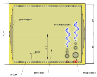
The design of the large-area SDD is illustrated in Figure 1(b). The Si tile is electrically divided in two halves, with two series of read-out anodes at the edges and the highest voltage along its symmetry axis (indicated as a solid line in Figure 1b). The drift length is 35 mm, and the drift field is 360 V cm-1, which corresponds to 1300 V maximum voltage. The drift velocity is then about 5 mm s-1 which translates in a maximum drift time of 7 s. The maximum size of the charge cloud reaching the anodes can be estimated using Equation 1 with mm (corresponding to an event absorbed at the bottom of the drift channel). This leads to about 1.3 mm (97% containment radius) at room temperature.
3 The ALICE heritage
The large area multi-anode SDD was initially designed in the framework of the LHC-ALICE experiment at CERN, and it demonstrated a spatial resolution better than 30 m in the two dimensions in localizing the impact point of ionizing particles[11]. The ALICE-D4 SDD features a sensitive area of 53 cm2, with the two detector halves read-out by means of two arrays of 256 anodes with 294 m pitch. These detectors were produced on 5-inch diameter, 300 m thick NTD (Neutron Transmutation Doped) Si wafers. Since 2008, 260 SDDs (for a total area of 1.37 m2) have successfully been in operation at ALICE.
Over the last few years R&D work has been carried out to characterize and optimize the same detector design for detection of soft X-rays. The preliminary results obtained under the XDXL INFN project (in collaboration with INAF, Politecnico di Milano, Università di Pavia) with a spare detector of ALICE with a bread-board read-out based on discrete electronics, showed high spectral performance and good position resolution already at room temperature. A preliminary evaluation of the spectroscopic and imaging performance of the ALICE Silicon Drift Detector performed at the INAF/IAPS X-ray facility[12] can be found in [13, 10, 14].
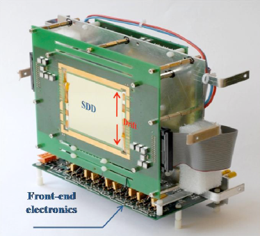
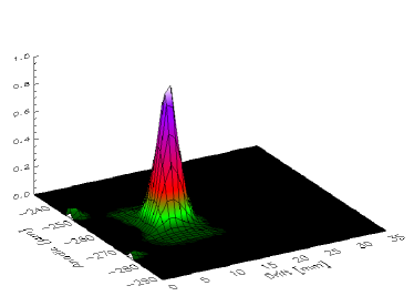
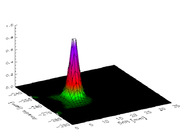
Figure 2 shows the SDD+FEE setup used in the measurements at the INAF/IAPS laboratory. Eight contiguous anodes of the SDD were separately connected to the same number of low gate capacitance JFETs (C pF) used as the input transistor of Amptek A250F-NF charge sensitive amplifiers. The feedback capacitor C fF and a reset transistor are both integrated on the JFET die, allowing to reduce the input stray capacitance for a better noise performance. Nonetheless, some stray capacitance is unavoidable due to the need to adapt the small SDD anode pitch to the much wider one of the electronics. Such a parasitic capacitance was estimated to be as high as 2.5 pF with the ALICE-spare detector set-up. Figure 3(a) shows the ALICE SDD (equipped with the discrete FEE) imaging capabilities at Troom for a 4.5 keV monochromatic X-ray beam (with a spot size of 100 m FWHM) as measured during the laboratory tests. It is worth noticing that, besides the noise performance of the discrete read-out electronics, also the small number of anodes (8) collecting the charge cloud introduces some systematics in the determination of the Gaussian cloud parameters (Equation 2), both with respect to the spectroscopic (see Figure 7 in [10]) and the imaging performance.
4 The SDD simulator
In order to estimate the spectroscopic and imaging capabilities of the Silicon Drift Detectors and to verify the consistence between the experimental results and the assumptions, we developed a Monte Carlo simulator written in IDL language and describing the charge drift and diffusion inside the SDD as well as the detector-FEE noise characteristics. A first version of the simulator, discussed in [13, 10, 14], allowed to model the ALICE-D4 SDD equipped with the 8-channels discrete FEE. The simulation results showed a very good agreement with the preliminary experimental measurements performed at , demonstrating the accuracy of the SDD modeling. In Figure 3(b) we show, as an example, the simulator output for the 8-channels discrete read-out at room temperature. This simulation was carried out considering the same experimental conditions of the measurement showed in Figure 3(a).
A new version of the simulator was then developed to study the performance obtainable by using an ASIC based FEE and by optimizing the SDD design (especially in regard to the anode pitch). The estimation of the imaging (and spectroscopic) capabilities of the SDD was carried out by means of simulations performed at different system temperatures and anode pitches. For these simulations, we considered a 32–channel integrated read-out (as baselined for the LOFT/WFM ASIC) and a noise figure consistent with the post-layout simulations of a test ASIC being developed within the XDXL project.The following scheme provides a step-by-step description of the simulator:
-
1.
A photon of energy is generated in a position (along drift direction) and (along anode direction) in the SDD;
-
2.
The photon is absorbed in the Silicon bulk and generates an electron cloud in (,). The estimation of the total charge in the cloud takes into account the average Silicon electron-hole pair generation energy (3.6 eV) and the Fano factor (0.115);
-
3.
The cloud, which can be assumed to have an initial width of , is propagated along the drift direction, reaching the read-out anodes with a width of , which is a function of the diffusion coefficient and of the drift time as described in Equation 1.
-
4.
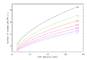
The electron cloud is then collected by a number of anodes depending on the width of the cloud and on the photon conversion point (,). The charge fraction which reaches each anode is described by Equation 2. Figure 4(a) shows the number of anodes collecting the electron cloud as a function of the photon absorption point along the drift direction for anode pitches from 145 m to 294 m with K and V cm-1.
-
5.
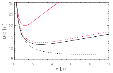
At this stage, the simulator takes into account the Equivalent Noise Charge (ENC) for each anode independently. The ENC is estimated considering an integrated FEE with the following characteristics: CR–RC shaper, C fF, C fF, and an available power per channel of 0.722 mW. The anode capacitance is estimated from the anode pitch and the detector thickness (between fF and fF for pitches in the range 145–294 m and 450 m thickness) while the leakage current is evaluated considering the intrinsic current measured in the laboratory plus the contribution due to the radiation damage after 5 years in orbit at 600 km altitude and 5∘ inclination, estimated by means of simulations performed with the ESA’s Space Environment Information System (SPENVIS, http://www.spenvis.oma.be). The dependence of the leakage current on the temperature is taken into account by considering the relation
(3) where is the absolute temperature, the electron charge, the Si bandgap (1.2–1.3 eV in the temperature interval K) and the Boltzmann’s constant. In Figure 4(b) we show the expected ENC at 0 ∘C and -20 ∘C for a 145 m pitch as a function of the shaping time for both the Beginning Of Life and the End Of Life cases. A Common Mode Noise (CMN), with an rms value of 25 e- is then added to the 32 ASIC channels. This CMN is due to the presence of noise on the detector bias line during the laboratory tests and can be reduced by proper filtering.
-
6.
The charge distribution is eventually fitted using Equation 2. The fitting parameters Qtot, y0 and (and ) allow to completely characterize the physical properties of the electron cloud (i.e. E, x0, y0).
| Anode Pitch | Detector | Photon | Position along | Position along |
|---|---|---|---|---|
| Temperature | Energy | drift direction (x) | anodic direction (y) | |
| 145 m | 293.15 K | 2.0 keV | 2.5 mm | 0 m |
| 175 m | 273.15 K | 2.5 keV | 5.0 mm | 50 m |
| 200 m | 253.15 K | 3.0 keV | 10.0 mm | 75 m |
| 225 m | 3.5 keV | 15.0 mm | 100 m | |
| 250 m | 6.0 keV | 20.0 mm | 150 m | |
| 294 m | 10.0 keV | 25.0 mm | ||
| 20.0 keV | 30.0 mm | |||
| 32.5 mm |
The simulations were performed exploring a large parameter space. Table 1 summarizes the different values used in the simulations concerning the anode pitch, the detector temperature, the incident photon energy and the photon absorption point in the anodic (y) and drift (x) coordinates.
5 Analysis of simulated data
For each simulation configuration we generated a large number () of photons. The output is saved as FITS tables, including a truncation of the values to simulate the ADC response. The event list containing the simulation results were then analysed fitting Equation 2 by means of a least squares minimization algorithm written in C (CMPFIT, http://www.physics.wisc.edu/~craigm/idl/cmpfit.html).
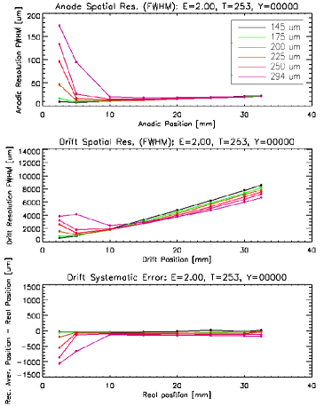
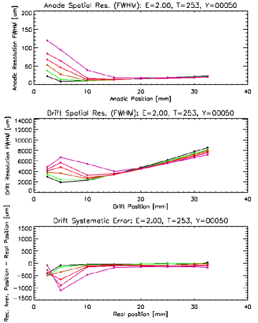
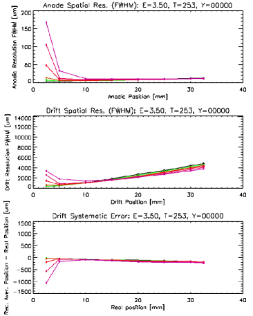
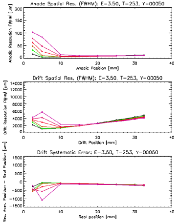
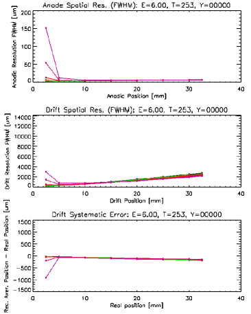
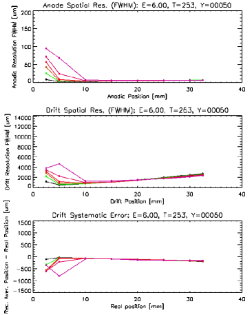
Figure 5(a) and Figure 5(b) show the anodic and drift spatial resolution (FWHM) for a 2 keV photon at 253 K for different anode pitches, for several photon absorption points in the drift direction and for two different positions in the anodic direction: at the center of the anode (y=0), and 50 m far from the anode center. The results shown in the plots indicate that a pitch smaller than 175 m is required to minimize the systematic effects on the position reconstruction introduced by the discretization of the charge cloud read-out and thus to optimize the detector spatial resolution at low energies (2.5–3.0 keV). For energies larger than 3 keV, the Signal-to-Noise ratio in each bin of the integrated Gaussian cloud increases, thus improving the spatial resolution as shown in Figure 5(c) and Figure 5(d) for Eph=3.5 keV and in Figure 6 for Eph=6.0 keV.
Looking at the simulation results in Figure 5 and Figure 6, is it clear that a small anode pitch translates in a better spatial resolution for photons absorbed in the first part (10–15 mm) of the drift channel. On the other hand, the dependence of the anodic and drift resolution on the pitch is less important at the end of the drift length and almost negligible for mm. Considering these results and the technological possibilities to build a SDD with a pitch smaller than 175 m, we suggest 145 m as the optimal pitch for the LOFT Wide Field Monitor.
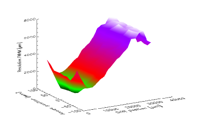
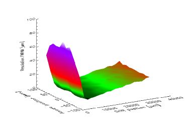
In order to characterize the detector spatial resolution with high precision we performed a new set of simulations with a fixed anode pitch of 145 m. In contrast to the simulations described above, this new set was performed by dividing each anode in 200 small sub-pixels, each with a surface of 14.5 m1.75 mm, and generating 103 photons of different energies (2.0, 2.5, 3.0, 4.5, 6.0, 10.0 and 20.0 keV) with a uniform spatial distribution inside the sub-pixel. In the left panel of Figure 7 we show the SDD spatial resolution FWHM (averaged on each sub-pixel) along the drift direction for 2 keV photons as a function of the absorption point in both the anodic and drift directions. In the right panel of the same figure we display the anodic spatial resolution. Such resolution is in general of the order of 20–30 m and, as expected, becomes comparable with pitch/2 when the electron cloud is completely collected by one single anode.
6 Discussion and conclusions
We developed a Monte Carlo simulator to study the effects of the charge diffusion on the spatial resolution of the SDDs. The simulated detector-FEE model takes into account all the most important factors which affect the detector imaging capabilities, investigating a number of configurations involving different detector designs and environmental conditions. The simulations have driven the design of the SDDs for the LOFT/WFM instrument, demonstrating that a pitch of 145 m is the optimal choice for maximizing the detector imaging performance. Such performance will be verified in the next months by using an ASIC-based FEE and the SDD prototypes already developed within the XDXL project in collaboration with Fondazione Bruno Kessler (FBK), Trento, Italy. With this design, extremely high spatial resolution (better than 70 m FWHM in the anodic direction) can be obtained by fitting the charge cloud distribution with a discrete Gaussian function. The same procedure also allows to determine the photon absorption point in the drift direction with a resolution (FWHM) better than 8 mm at 2 keV, 5 mm at 3.5 keV and 3 mm at 6 keV. The Silicon Drift Detectors can thus be effectively used as a soft (E2 keV) X-ray imaging detector, allowing to perform bi-dimensional photon-by-photon imaging in the energy range 2–50 keV, with low resource requirements in term of power, weight and complexity of the read-out electronics.
Acknowledgements.
The Italian team is grateful for support by ASI, INAF and INFN.References
- [1] Feroci, M., Stella, L., van der Klis, M., Courvoisier, T. J.-L., Hernanz, M., Hudec, R., Santangelo, A., Walton, D., Zdziarski, A., Barret, D., Belloni, T., Braga, J., Brandt, S., Budtz-Jørgensen, C., Campana, S., den Herder, J.-W., Huovelin, J., Israel, G. L., Pohl, M., Ray, P., Vacchi, A., Zane, et al., “The Large Observatory for X-ray Timing (LOFT),” Experimental Astronomy , 100 (Aug. 2011).
- [2] Feroci, M., Costa, E., Soffitta, P., Del Monte, E., di Persio, G., Donnarumma, I., Evangelista, Y., Frutti, M., Lapshov, I., Lazzarotto, F., Mastropietro, M., Morelli, E., Pacciani, L., Porrovecchio, G., Rapisarda, M., Rubini, A., Tavani, M., and Argan, A., “SuperAGILE: The hard X-ray imager for the AGILE space mission,” Nuclear Instruments and Methods in Physics Research A 581, 728–754 (Nov. 2007).
- [3] Feroci, M., Costa, E., Del Monte, E., Donnarumma, I., Evangelista, Y., Lapshov, I., Lazzarotto, F., Pacciani, L., Rapisarda, M., Soffitta, P., di Persio, G., Frutti, M., Mastropietro, M., Morelli, E., Porrovecchio, G., Rubini, A., Antonelli, A., Argan, A., Barbiellini, G., Boffelli, F., Bulgarelli, A., Caraveo, P., Cattaneo, P. W., Chen, A. W., Cocco, V., Colafrancesco, S., Cutini, S., D’Ammando, F., de Paris, G., Di Cocco, G., Fanari, G., Ferrari, A., Fiorini, M., Fornari, F., Fuschino, F., Froysland, T., Galli, M., Gasparrini, D., Gianotti, F., Giommi, P., Giuliani, A., Labanti, C., Liello, F., Lipari, P., Longo, F., Mattaini, E., Marisaldi, M., Mauri, A., Mauri, F., Mereghetti, S., Moretti, E., Morselli, A., Pellizzoni, A., Perotti, F., Piano, G., Picozza, P., Pilia, M., Pittori, C., Pontoni, C., Preger, B., Prest, M., Primavera, R., Pucella, G., Rappoldi, A., Rossi, E., Sabatini, S., Santolamazza, P., Tavani, M., Stellato, S., Tamburelli, F., Traci, A., Trifoglio, M., Trois, A., Vallazza, E., Vercellone, S., Verrecchia, F., Vittorini, V., Zambra, A., Zanello, D., and Salotti, L., “Monitoring the hard X-ray sky with SuperAGILE,” A&A 510, A9 (Feb. 2010).
- [4] Fenimore, E. E. and Cannon, T. M., “Coded aperture imaging with uniformly redundant arrays,” Appl. Opt. 17, 337–347 (Feb. 1978).
- [5] Fenimore, E. E. and Cannon, T. M., “Uniformly redundant arrays - Digital reconstruction methods,” Appl. Opt. 20, 1858–1864 (May 1981).
- [6] Vacchi, A., Castoldi, A., Chinnici, S., Gatti, E., Longoni, A., Palma, F., Sampietro, M., Rehak, P., and Kemmer, J., “Performance of the UA6 large-area silicon drift chamber prototype,” Nuclear Instruments and Methods in Physics Research A 306, 187–193 (Aug. 1991).
- [7] Rashevsky, A., Bonvicini, V., Burger, P., Piano, S., Piemonte, C., and Vacchi, A., “Large area silicon drift detector for the ALICE experiment,” Nuclear Instruments and Methods in Physics Research A 485, 54–60 (June 2002).
- [8] Gatti, E. and Rehak, P., “Semiconductor drift chamber – An application of a novel charge transport scheme,” Nuclear Instruments and Methods in Physics Research 225, 608–614 (Sept. 1984).
- [9] Gatti, E., Longoni, A., Rehak, P., and Sampietro, M., “Dynamics of electrons in drift detectors,” Nuclear Instruments and Methods in Physics Research A 253, 393–399 (Jan. 1987).
- [10] Zampa, G., Campana, R., Feroci, M., Vacchi, A., Bonvicini, V., Del Monte, E., Evangelista, Y., Fuschino, F., Labanti, C., Marisaldi, M., Muleri, F., Pacciani, L., Rapisarda, M., Rashevsky, A., Rubini, A., Soffitta, P., Zampa, N., Baldazzi, G., Costa, E., Donnarumma, I., Grassi, M., Lazzarotto, F., Malcovati, P., Mastropietro, M., Morelli, E., and Picolli, L., “Room-temperature spectroscopic performance of a very-large area silicon drift detector,” Nuclear Instruments and Methods in Physics Research A 633, 15–21 (Mar. 2011).
- [11] Crescio, E. and Nouais, D., “Electron cloud size measurement in silicon drift detectors and spatial resolution improvement,” Nuclear Instruments and Methods in Physics Research A 564, 475–481 (Aug. 2006).
- [12] Muleri, F., Soffitta, P., Bellazzini, R., Brez, A., Costa, E., Frutti, M., Mastropietro, M., Morelli, E., Pinchera, M., Rubini, A., and Spandre, G., “A versatile facility for the calibration of x-ray polarimeters with polarized and unpolarized controlled beams,” in [Society of Photo-Optical Instrumentation Engineers (SPIE) Conference Series ], Society of Photo-Optical Instrumentation Engineers (SPIE) Conference Series 7011 (Aug. 2008).
- [13] Zampa, G., Vacchi, A., Feroci, M., Labanti, C., Bonvicini, V., Rashevsky, A., Zampa, N., Campana, R., Del Monte, E., Evangelista, Y., Muleri, F., Pacciani, L., Rubini, A., Soffitta, P., Costa, E., Donnarumma, I., Lazzarotto, F., Mastropietro, M., Morelli, E., Rapisarda, M., Fuschino, F., Marisaldi, M., Baldazzi, G., Picolli, L., Grassi, M., and Malcovati, P., “X-ray imaging and spectroscopy performance of a large area silicon drift chamber for wide-field x-ray astronomy applications,” in [Society of Photo-Optical Instrumentation Engineers (SPIE) Conference Series ], Society of Photo-Optical Instrumentation Engineers (SPIE) Conference Series 7732 (July 2010).
- [14] Campana, R., Zampa, G., Feroci, M., Vacchi, A., Bonvicini, V., Del Monte, E., Evangelista, Y., Fuschino, F., Labanti, C., Marisaldi, M., Muleri, F., Pacciani, L., Rapisarda, M., Rashevsky, A., Rubini, A., Soffitta, P., Zampa, N., Baldazzi, G., Costa, E., Donnarumma, I., Grassi, M., Lazzarotto, F., Malcovati, P., Mastropietro, M., Morelli, E., and Picolli, L., “Imaging performance of a large-area Silicon Drift Detector for X-ray astronomy,” Nuclear Instruments and Methods in Physics Research A 633, 22–30 (Mar. 2011).