Effect of dielectric confinement on energetics of quantum metal films
Abstract
We suggest a method for the self-consistent calculations of characteristics of metal films in dielectric environment. Within a modified Kohn-Sham method and stabilized jellium model, the most interesting case of asymmetric metal-dielectric sandwiches is considered, for which dielectric media are different from the two sides of the film. As an example, we focus on Na, Al and Pb. We calculate the spectrum, electron work function, and surface energy of polycrystalline and crystalline films placed into passive isolators. We find that a dielectric environment generally leads to the decrease of both the electron work function and surface energy. It is revealed that the change of the work function is determined only by the average of dielectric constants from both sides of the film.
pacs:
73.22.Dj, 73.40.Ns, 73.40.Vz, 68.03.CdI INTRODUCTION
Thin metal films and flat islands on semiconductor or dielectric substrates can be considered as two-dimensional electron systems with properties, which are of interest both from the fundamental point of view and from the perspective of their application in nanoscale electronic devices.
There are a limited number of experimental works focused on quantum size effects in such systems (for reviews, see Otero ; 14. ; BUUUU ; LLLLLLL ; TAAAA ; VAAAA ; Viiii ; CHHHH ; Chuu ) due to difficulties in sample fabrication, as well as because of lack of suitable experimental methods. One of the most important characteristics of metal nanostructures is electron work function.
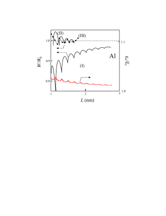
There are different methods, which enable one to calculate electron structure of slabs consisting of few monoatomic layers. Let us combine them into three groups according to the complexity of computations: I – the Sommerfeld electrons in-a-box model (analytical calculations, slabs and wires) 1. ; 2. ; PKV ; Han ; KuPo ; ddddddd ; II – self-consistent calculations within various versions of jellium model (slabs and wires) Schulte ; 11. ; Fiolhais2000 ; Smog ; Horowitz2009 ; III – ab initio calculations (slabs) 8. ; 9. ; ZHHHH ; 10. . The obtained results are illustrated in figure 1 for all these three groups. An important ingredient of approaches within group III is the monolayer number in the film (see dots in figure 1). For groups I and II, changes continuously.
In group I, the Fermi energy (kinetic energy) is counted from the flat bottom of conductivity band, while the work function is counted from the vacuum level. Therefore, their size dependencies are “asymmetric”. In addition to quantum oscillations, these quantities contain monotonic size contributions, which, at small film thicknesses, together show up through inequalities and , where and correspond to the three dimensional (3D) metal (allowing for the energy counting for ).
In pppppp ; 1996 , an asymptotic behavior of electron chemical potential for spherical clusters of radius was determined, from which it follows that
| (1) |
where for simple metals, . It is expectable that such a monotonic contribution must appear for films also. However, in contrast to the case of group I, self-consistent calculations of groups II and III (see figure 1), at small film thickness, point out to the suppression of monotonic dependence (having an asymptotic (1)) by corrections of higher orders of smallness. For instance, compensation of terms occurs at , and is large, provided .
Experimental results also do not allow to draw unambiguous conclusions on the character of monotonic component of : in experiments BUUUU , it is absent (Yb films on Si substrate), while, according to 14. ; TAAAA , it coincides with the one of group I. Note that the comparison of a measured work function for the sandwich consisting of Ag film on Fe(100) in 14. ; TAAAA with calculated results for slabs in vacuum is rather relative.
Work function as well as film surface energy in dielectric environment have never been calculated before. The aim of this work is to compute energy characteristics of metal films in dielectrics. We suggest a method for self-consistent calculations of equilibrium profiles of electron concentration, effective potential, energy spectrum, and integral characteristics of metal films in dielectrics and dielectric substrates. The developed method is based on a stabilized jellium model PTS and local density approximation for exchange-correlation potential Per-Zug , which were used by us before Bab-2008 to analyze characteristics of semi-infinite metal with dielectric coating.
This paper is organized as follows. In Section II, we formulate our model. In Section III, we presents our main results and provide a discussion of them. We conclude in Section IV.
II MODEL
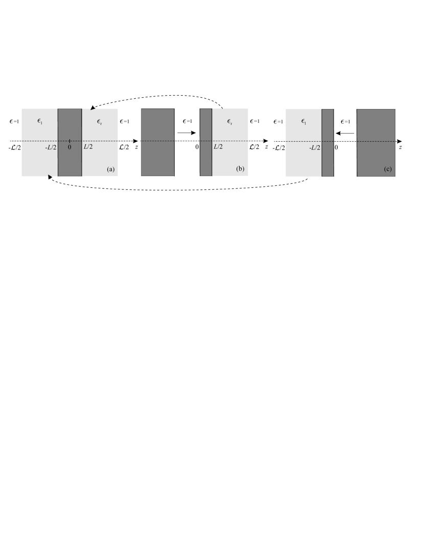
Let us consider a metallic film of thickness at zero temperature. We direct axis perpendicularly to the film surface (figure 2 (a), ).
Principal identities for the film can be obtained within a model of a rectangular well for conduction electrons. To perform a preliminary analysis, we suppose that the bottom of the potential well is flat and we count energies starting from its value. Final expression for the kinetic energies of conduction electrons depends only on energy differences; therefore, energies counting in such a way is allowed.
We study a film of thickness comparable in magnitude to the Fermi wavelength of an electron in 3D metal. The longitudinal sizes of the sample are assumed to be considerably larger than the film thickness (), which leads to the pronounced quantization of the transverse component of the electron momentum. The three-dimensional Schrodinger equation for a quantum box can be separated into one-dimensional equations.
The eigenenergies are given by
| (2) |
where is the eigenvalue of the -th perpendicular state (hereafter the Hartree atomic units are used: ). The eigenvalue is the bottom of the -th subband. For finite and periodic systems in the z-direction Dirichlet and periodic boundary conditions are used, respectively. Therefore, possible allowed electron states form a system of parallel planes in the space, (see figure 3).
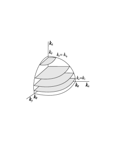
Occupation of electron states starts from the point and follows an increase of radius-vector. As a result, it turns out that all the occupied states are contained within the area of space, confined between the plane and semi-sphere of radius .
The number of states in each of the circles, formed by the intersection of Fermi semi-sphere with planes of area , within the interval of wave vectors and taking into account both possible spin projections, is
The maximum value of in each circle numbered by , is equal to the circle radius . In order to find the number of the occupied states, which coincides with the number of valence electrons in the film, one should integrate over in each circle, and then sum up contributions of all the circles:
| (3) |
Taking into account an expression for electron kinetic energy , the total kinetic energy of electron subsystem equals
| (4) |
where is the number of the last occupied or partially occupied subband.
In the frame of density-functional theory and stabilized jellium model (SJ), the total energy of metal sample is represented by the functional of nonhomogeneous electron concentration :
| (5) |
where is the (non-interacting) electron kinetic energy, is the exchange-correlation energy, is the Hartree (electrostatic) energy, is the pseudopotential (Ashcroft) correction, and is the Madelung energy. The sum of first three terms in expression (5) corresponds to the energy of “ordinary” jellium, . The average energy per valence electron in the bulk of metal is , where is a total number of free electrons of concentration , defined by valence and atomic density.
The positive (ionic) charge distribution can be modeled by the step function
| (6) |
Solving the Kohn-Sham equations
| (7) |
| (8) |
together with the Poisson equation
| (9) |
with the step function
| (10) |
we obtain the single electron wave function and the eigenvalue self-consistently.
We use exchange-correlation potential in LDAPer-Zug . The term in (8), which makes it possible to distinguish different crystal faces, represents the difference between the potential of the ionic lattice and the electrostatic potential of the positively charged background averaged over the Wigner-Seitz cell:
where is the distance between the atomic planes parallel to the surface. The term describes a polycrystalline sample PTS . In equation (10) and are dielectric constants of isolators from the left and right side of the film, respectively.
The electron density profile is expressed through the wave functions
| (11) |
Values of and are determined by the solution of the equation
| (12) |
which follows from the normalization condition (3) and definition of the Fermi energy.
In nanofilms, Friedel oscillations are significant throughout the sample. Therefore, energies are counted from the vacuum level, which is the energy of the electron in rest in the area . For bound states, energies are negative, including .
We use iterative procedure (see Appendix A) allowing us to solve self-consistently the system of equations (7), (9), (11) and to find optimal profiles , , as well as spectrum of one-particle energies. As a result, work function is defined in the form
| (13) |
Let us consider a scheme for the surface energy determination (see figure 2 (b) and (c)) for the film of thickness in a dielectric environment.
First, we take a semi-infinite metal (Me∞) covered by a dielectric (). Let us denote the energy of such a sample as . We now split the sample and move the parts, as shown in figure 2 (b). As a result, two new surfaces of the same area are formed, which are in a contact with the vacuum (). We denote the energies of these two parts as and , while the irreversible work , which is needed to form them, as
| (14) |
Let us stress that, as a result of these manipulations, the “fabricated” sandwich represents a film of thickness on the dielectric substrate in vacuum (air).
Similar manipulations with another sample (figure 2 (c)) require a work
| (15) |
It is convenient to represent the total energy as a sum of bulk and surface contributions
Then, bulk components do compensate in the expressions (14) and (15). In each case considered above, the specific surface energy equals .
The work needed to “create” a film on a dielectric is
| (16) |
Now, we join two sandwiches by their free surfaces. We then obtain a film shown in figure 2 (a). The work to create it can be represented as the energy of adhesion of such two pieces with the minus sign
| (17) |
Electron density profiles and potentials for each of the contributions in the expressions (16) and (17) are different, so that they must be calculated self-consistently and separately.
As similar to the definition for the semi-infinite metal LK ; Bab-2008 , for the film is determined by the difference between the total film energy (5) and the energy of homogeneous metal (stabilized jellium) of the same volume:
| (18) |
By using equation (4), quantum-mechanical definition of an energy
as well as the definition given by equation (18), we obtain an expression for the first component of :
| (19) |
where is the kinetic energy per 1 electron for bulk. The remaining components are
| (20) |
| (21) |
For asymmetric sandwiches, , due to the formal division on the doubled area, the surface energy is calculated “in average”. This is the consequence of the definition of through the integral of tangential component of pressure tensor over from to . The pressure tensor contains the nonelectrostatic part and the Maxwell stress tensor (cf e.g. Pg-2006 ).
III Results and discussion
We perform calculations for both polycrystalline and crystalline films made of Na, Al and Pb, with electron concentration with corresponding electron parameter 3.99, 2.07 and 2.30 .
The minimal thickness of “crystalline” sandwiches should be not less than . It must be equal to for , only in the case Eq. (17) is used. d is comparable to (, 6.78 and 7.53 for Na, Al and Pb, respectively).
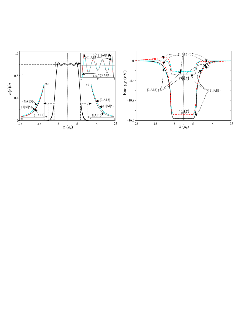
In view of the multimolecular thicknesses of dielectric coatings on the metal film surfaces and rapid fall of the electron distribution outside of a film (approximately at a distance of 10 – 15 ), we formally neglected the effect of a thickness of the coatings, whose minimum thicknesses must be much greater than that of a monatomic (molecular) layer of a dielectric. For comparison, we recall that the diameter of atom Si equals 5 . If the thicknesses of the dielectrics on the surfaces of the metal film are foreseen to be less than the free path of an electron (tens of angstrom) injected into these dielectrics, then the calculated work function is qualitatively appropriate for the vacuum-dielectric-metal slab-dielectric-vacuum.
For symmetric sandwich the effect of a dielectric coating on the surfaces is reduced to the “elongation” of the electron distribution tail and the effective potential beyond the surface of a metal (polycrystalline films and on Fig. 4). The calculations were performed for . Inside the film one can see the Friedel oscillations of electron density with peaks near geometrical boundaries. The period of oscillations is close to and only weakly depends on the presence of dielectric coatings. The situation is similar for Na and Pb films.
At the boundaries between the metal film and the coatings, there are jumps in the derivative of the electrostatic potential , which disappear, provided the dielectric constants of the coatings are equal to 1. These jumps are due to the boundary conditions (23) at . The jumps are also reflected on profile, since is one of its components. In addition, at the borders, there are another jumps of not only the derivative , but also of profile itself for any values of , including . Such jumps have another origin compared to the first ones. This fact is linked to some features of the model PTS , namely to the presence of the effective potential component . These nonphysical jumps should not be taken into account in the estimation of the effective force
It is seen from figure 4 that force orientations are opposite at both sides of the film, so that the film in whole must be stressed. The existence of the force should lead to the increase of spacings between some lattice planes , while spacings between other planes must become narrower.
The depth of the potential well , in which the electrons are located in metal film, decreases “in average” with increasing and, as a result, the electron work function also decreases (see figure 6).
Film spectra are presented in figure 5. For comparison, in the same figure, we also provide the results obtained within the electrons-in-a-box model with the well depth .
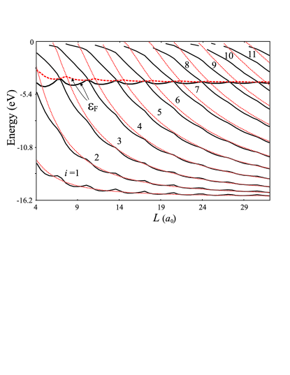
It is seen from figure 5 that the dependence of the eigenstate energies on the film thickness, within the SJ model, is oscillating and decreasing. For subbands with large numbers , there are gaps due to the algorithm instability in the vicinity of the vacuum level. Within the rectangular-box model, this dependence is only decreasing. Due to smoother edges of the self-consistent well, it contains more subbands compared to the model of a rectangular box. Difference in subbands numbers significantly affects calculated dielectric function and optical conductivity of the nanofilm KuPo .
Within the rectangular-box model, in contrast to the SJ model, is always located above one for 3D metal. Amplitudes of oscillations decrease as increases. Within both models, maximum Fermi energies (minimum work functions (13)) correspond to the points, in which curves of eigenenergies intersect Fermi energies. Within the SJ model, in contrast to the rectangular-box model, minimum Fermi energies correspond to the points, in which Fermi energy is located between two nearest eigenenergies (magic film thicknesses similar to magic numbers in clusters).
Asymmetric sandwiches and , which contacts the air or vacuum, are of particular interest from the viewpoint of experimental investigation due to the perspective of their use in technological applications. For instance, these are films on Si () or Ge () substrates with different concentration of impurities and crystallographic orientations (see, e.g. TAAAA ).
Let us consider both electron density and potential profiles for the polycrystalline film . Presence of a dielectric at the right side of the film leads to the asymmetry of electron distribution (see the insets in figure 4), so that there appears a hump in both the electrostatic and effective potential at the left side above the vacuum level. This should result, for example, in the anisotropy of a field emission along the axis. It is worth mentioning that bottoms of wells for sandwiches and are essentially the same, some difference appears only in “tails” of potential profiles.
It is of interest to compare heights of humps at and 20, 22, 23.5 . These thicknesses correspond to the minimum, maximum, minimum of the dependence for . It turns out that, with the increase of , the hump height weakly oscillates and decays similarly to the work function, but maxima of the hump height corresponds to minima of the . For the values of , as given above, these heights are 0.176, 0.148, 0.170 and 0.158, 0.139, 0.156 eV, respectively.
In order to analyze such a behavior of potential profiles, it is necessary to go beyond the isotropic model based on a defined (6) distribution of homogeneous positively charged background, i.e. one has to take into account not only the reaction of the electron subsystem, but also the reaction of the ion subsystem to the presence of a dielectric. Spacings between the lattice planes are determined by the balance of forces from the right and left sides for each plane. A simplest realization of this idea is to disregard variations of spacings between the lattice planes and to vary the profile of the ion jellium distribution (6). We found that such a procedure leads to a significant deformation of the well bottom, but does not result to considerable changes of both the spectrum and hump height.
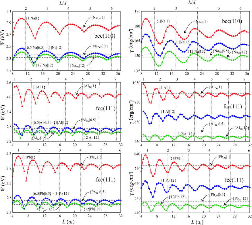
Figures 6 show results of our calculations of both the electron work function and surface energy for crystalline sandwiches using expression (18). Horizontal lines correspond to semiinfinite samples. In contrast to the surface energy, size dependences have deep and pronounced minima. It is easier to analyze them using a simple model PKV . Amplitudes of largest work function “oscillations” are smaller than 0.5 eV. By considering dependencies for different metals, it is easy to see that all the differences are due to values of . For the Al, which has the smallest , work function oscillations are maximum, while the period is minimum. Positions of both maxima and minima depend weakly on of a dielectric and slightly shift towards smaller with the increase of .
In contrast to the work function, surface energy oscillations can be approximated by analytical dependences
with parameters and . Maxima of function , correspond to “magic” film thicknesses, which are defined by maximum occupation of a given subband.
The unexpectable result of self-consistent calculations is a coincidence of dependencies for sandwiches and . Computations for and give a similar result. This means that the electron work function for asymmetric sandwiches coincides with high accuracy with the work function for symmetric sandwiches with the averaged value .
Work function has both the bulk and surface contributions. Because bulk metal contributions for sandwiches and are the same by definition, also the same are contributions of dipole surface barriers. We here imply the total contribution of both sides of a sandwich, since the work function is an “isotropic” characteristics25a . A coincidence of work functions is most likely a geometric effect. This feature will be addressed elsewhere.
IV CONCLUSIONS
We proposed a method for the self-consistent calculations of spectra, electron work function, and surface energy of metal films placed into passive dielectrics. As typical examples, we considered Na, Al, and Pb films.
The effective force acting on the film from the outside is due to the inhomogeneous electron distribution. This force should lead to film stressing in a transverse direction. The effect of the stressing generally becomes more significant with the increase of the film thickness.
In contrast to the surface energy, size dependencies of work function have deep and strongly pronounced minima. The smaller the more difficult the problem of numerical analysis of size dependencies in the vicinities of these minima.
With the increase of film thickness up to few , size variations of both the work function and surface energy occur near their average values (for symmetric sandwiches, these values correspond to 3D metals and do not contain significant monotonous size contributions). Dielectric environment generally leads to the decrease of electron work function and surface energy.
We also considered asymmetric metal-dielectric sandwiches characterized by different dielectrics at both sides of the film. One of the examples of such systems is a film on the dielectric substrate. We found that the presence of a dielectric from one side of the film leads to such a “deformation” of electron distribution that there appears a “hump” above the vacuum level both in the electrostatic and effective potentials. The asymmetry of potential profile of this kind should lead to an anisotropy of the field emission. In addition to size dependencies, the shift of the work function is generally determined by the average dielectric constants of environments.
Obtained wave electron functions for metal-dielectric sandwiches allow us to calculate the matrix elements of optical transitions, conductivity tensor, and coefficient of optical absorptionKuPo .
Acknowledgements.
We thank W. V. Pogosov for reading the manuscript.Appendix A Self-consistency procedure
The initial approximation is chosen for solving the Kohn-Sham equations in the form of a one-parametric trial function , where
is the variational parameter, which is found through the minimization of surface energy. Solution by a direct variational method is an independent problem, which is not addressed in this paper (for simple metals is closed to ). As a result of integration of equation (9), within the initial approximation, we obtain .
Each wave function is constructed as
under the condition of continuity of functions , as well as of their derivatives . is an arbitrary point in the interval , while and are functions, which are found by a numerical solution of Eq. (7) by the Numerov‘s method from to and from to , respectively. It is sufficient to take values . In these points, the potential profile is cut off. The boundary conditions (7) here are determined by the behavior of the wave function under the barrier from the left () and right () sides from the slab (), respectively. Boundary conditions provide wave function, as well as its derivative at . This peculiarity of our computations is due to the fact that errors of the numerical method for the wave function and near the right and left boundaries of the interval grow, since the round-off errors also increase and lead to the instability of the algorithm under the motion towards the exponential damping.
In order to solve the system of equations (7), (9) and (11) self-consistently, with relatively small number of iteration steps, the Poisson equation (9) should be modified, in particular, by introducing a perturbation Man1975 .
Equation (9) is solved by the Lagrange method in the form
| (22) |
with the boundary conditions
| (23) |
The term was introduced as a small perturbation; and are potentials outside and inside the film, respectively. In equation (22), at each step of the iteration , electrostatic potential profile depends not only on the electronic concentration profile, but also on its own profile at the previous iteration. It is convenient to take equal to electron wave number at the Fermi sphere of homogeneous electron liquid.
The solution of equation (22) for has the simple form
| (24) |
where and for , respectively. The choice of values and immediately follows from the condition of finiteness of potentials far away from the film.
Let‘s introduce notation
| (25) |
where . Then for and for .
In the case of the symmetric sandwich the accurateness of calculations is verified by examination the stationarity conditions and in the center of the slab ().
References
- (1) R. Otero, A. L. Vazquez de Parga, and R. Miranda, Phys. Rev. B 66, 115401 (2002).
- (2) J. J. Paggel, C. M., Wei, M. Y. Chou, D.-A. Luh, T.Miller, and T.-C. Chiang, Phys. Rev. B 66, 233403 (2002).
- (3) D. V. Buturovich, M. V. Kuz’min, M. V. Loginov and M. A. Mittsev, Fiz. Tverdogo Tela 48, 2085 (2006) [Phys. Solid State, 48, 2205 (2006)]; Fiz. Tverdogo Tela 50, 354 (2008) [Phys. Solid State, 50, 173 (2008)].
- (4) Y. Liu, J. J. Paggel, M. H. Upton, T. Miller, and T.-C. Chiang, Phys. Rev. B 78, 235437 (2008).
- (5) T.-C. Chiang, AAPPS Bullet. 18, 2 (2008).
- (6) A. L. Vazquez de Parga, J. J. Hinarejos, F. Calleja, J. Camarero, R. Otero, and R. Miranda, Surf. Sci. 603, 1389 (2009).
- (7) N. A. Vinogradov, D. E. Marchenko, A. M. Shikin, V. K. Adamchuk, and O. Rader, Fiz. Tverdogo Tela 51, 1121 (2009) [Phys. Sol. State 51, 179 (2009)].
- (8) P.-W. Chen, Y.-H. Lu, T.-R. Chang, C.-B. Wang, L.-Y. Liang, C.-H. Lin, C.-M. Cheng, K.-D. Tsuei, H.-T. Jeng, and S.-J. Tang, Phys. Rev. B 84, 205401 (2011).
- (9) E. Ogando, N. Zabala, E. V. Chulkov, M. J. Puska, Phys. Rev. B 71, 205401 (2005).
- (10) J. P. Rogers III, P. H. Cutler, T. E. Feuchtwang, and A. A. Lucas, Surf. Sci. 181, 436 (1987).
- (11) M. V. Moskalets, Pis‘ma Zh. Eksp. Teor. Fiz. 62, 702 (1995) [JETP Lett. 62, 719 (1995)].
- (12) V. V. Pogosov, V. P. Kurbatsky, and E. V. Vasyutin, Phys. Rev. B 71, 195410 (2005).
- (13) Y. Han and D.-J. Liu. Phys. Rev. B 80, 155404 (2009).
- (14) V. P. Kurbatsky and V. V. Pogosov, Phys. Rev. B 81, 155404 (2010).
- (15) V. D. Dymnikov, Fiz. Tverdogo Tela 53, 847 (2011) [Phys. Sol. State 53, 901 (2011)].
- (16) F. K. Schulte, Surf. Sci. 55, 427 (1976).
- (17) N. Zabala, M. J. Puska and R. M. Nieminen, Phys. Rev. B 59, 12652 (1999).
- (18) I. Sarria, C. Henriques, C. Fiolhais, and J. M. Pitarke, Phys. Rev. B 62, 1699 (2000).
- (19) A. N. Smogunov, L. I. Kurkina, and O. V. Farberovich, Fiz. Tverdogo Tela 42, 1848 (2000) [Phys. Sol. State 42, 1898 (2000)].
- (20) C. M. Horowitz, L. A. Constantin, C. R. Proetto, and J. M. Pitarke, Phys. Rev. B 80, 235101 (2009).
- (21) P. J. Feibelman and D. R. Hamann, Phys. Rev. B 29, 6463 (1984).
- (22) J. C. Boettger, Phys. Rev. B 53, 13133 (1996).
- (23) Z. Zhang, Q. Niu and C.-K. Shih, Phys. Rev. Lett. 80, 5381 (1998).
- (24) A. Kiejna, J. Peisert, and P. Scharoch. Surf. Sci. 432, 54 (1999).
- (25) V. V. Pogosov, Sol. St. Commun. 75, 469 (1990).
- (26) A. Kiejna and V. V. Pogosov, J. Phys.: Cond. Matter 8 4245 (1996).
- (27) J. P. Perdew, H. Q. Tran, and E. D. Smith, Phys. Rev. B 42, 11627 (1990).
- (28) J. P. Perdew and A. Zunger, Phys. Rev. B 23, 5048 (1981).
- (29) A. V. Babich and V. V. Pogosov, Surf. Sci. 603, 2393 (2009).
- (30) J. Arponen, P. Hautojärvi, R. Nieminen, and E. Pajanne, J. Phys. F 3, 2092 (1973).
- (31) N. D. Lang, W. Kohn, Phys. Rev. B 3, 6010 (1973).
- (32) V. V. Pogosov, Chem. Phys. Lett. 193, 129 (1992).
- (33) V.V. Pogosov, V.P. Kurbatsky, Zh. Eksp. Teor. Fiz. 119 (2001) 350 [J. Exp. Theor. Phys. 92 (2001) 304].