Edge state transport through disordered graphene nanoribbons in the quantum Hall regime
Abstract
The presence of strong disorder in graphene nanoribbons yields low-mobility diffusive transport at high charge densities, whereas a transport gap occurs at low densities. Here, we investigate the longitudinal and transverse magnetoresistance of a narrow (60 nm) nanoribbon in a six-terminal Hall bar geometry. At 11 T, quantum Hall plateaux appear at , and , for which the Landau level spacing is larger than the Landau level broadening. Interestingly, the transport gap does not disappear in the quantum Hall regime, when the zero-energy Landau level is present at the charge neutrality point, implying that it cannot originate from a lateral confinement gap. At high charge densities, the longitudinal and Hall resistance exhibit reproducible fluctuations, which are most pronounced at the transition regions between Hall plateaux. Bias-dependent measurements strongly indicate that these fluctuations can be attributed to phase coherent scattering in the disordered ribbon.
pacs:
73.23.-b, 72.80.Vp, 73.43.QtSince the discovery of graphene 05-NOV_05-ZHA , the investigation of transport through low-dimensional graphene structures, such as nanoribbons and quantum dots, has obtained much attention 11-MOL . Whereas graphene is a gapless material system, size quantization effects in narrow structures are expected to open a bandgap 96-NAK_06-BRE_06-SON . Moreover, depending on the precise edge structure and interaction effects, peculiar edge states are predicted to appear 96-NAK_06-BRE_06-SON ; 96-FUJ_06_SON_07-RYC_07-TRA . Transport measurements on ribbons have shown, however, that the presence of bulk and edge disorder obscures the observability of bandgap and edge state related transport properties 11-MOL .
Strong edge disorder gives rise to enhanced intervalley scattering in narrow ribbons EdgeDisorder_Theory . This results in a suppression of the carrier mobility in the high-density regime, and the occurrence of a transport gap in the low-density regime. A transport gap appears due to the confinement of charges, for which different origins have been proposed, e.g., the occurrence of a strong localization regime 10-HAN_10-OOS or the presence of disorder-induced electron and hole puddles which are separated by a bandgap 09-STA_09-TOD_10-GAL . At high density, the charge carriers are delocalized and propagate diffusively through a disordered ribbon. Although transport through magnetoelectric subbands has been predicted in narrow ribbons with well-defined edges 06-PER_06-BRE , experiments have shown that the presence of strong disorder impedes the occurrence of conductance quantization at zero magnetic field 08-LIN_10-LIA_11-TOM and the development of quantum Hall edge states at high field 11-RIB_12-MIN_12-HET . Profound knowledge of disorder effects on transport is therefore needed to get a better understanding of the electronic properties of low-dimensional graphene structures.
Here we present a systematic study of electronic transport through a 60 nm wide graphene nanoribbon in a six-terminal Hall bar geometry. Our transport measurements show that the transport gap at low charge density does not disappear in the quantum Hall regime, and therefore, shows that a bandgap due to lateral confinement does not play a crucial role in the formation of the transport gap at high magnetic field. Outside the transport gap, the measurements at the highest applied magnetic field ( T) only reveal the quantum Hall plateaux at , and , for which the corresponding Landau level spacing is larger than the estimated Landau level broadening. Moreover, the longitudinal and Hall resistance exhibit aperiodic fluctuations, which are most pronounced in the transition regions between the quantum Hall plateaux. Since these reproducible fluctuations are strongly suppressed when the bias and thermal energy are larger than the estimated Thouless energy, they can be mainly attributed to quantum interference effects in the disordered ribbon.
Exfoliated single-layer graphene flakes are transferred to a highly p-doped Si substrate containing a 285 nm SiO2 top layer. After deposition of Ti/Au electrodes onto the graphene, the flakes are etched in an Ar/O2 plasma to obtain narrow nanoribbons (width nm) in a six-terminal Hall bar geometry (Fig. 1a). The etched structures are cleaned at C in forming gas to reduce the amount of contamination at the graphene surface. The transport experiments are carried out in an Oxford dilution refrigerator at temperatures of 30 mK and 4.2 K. The longitudinal and transverse resistance are measured as function of current bias (), gate-voltage () and magnetic field () by using standard lock-in detection techniques. We discuss the data of a device consisting of a ribbon with length nm and width nm (these data are representative for the other measured devices of similar dimensions).
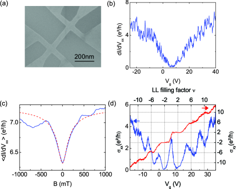
First we discuss the transport characteristics of the device at K. The differential conductance () versus gate voltage (Fig. 1b) clearly shows a suppressed conductance at low density in the vicinity of the Dirac point ( V), as is characteristic for graphene nanoribbon devices 11-MOL . At high electron ( V) and hole density ( V), we observe reproducible conductance fluctuations. In this regime, the field-effect mobility of the charge carriers is cm2/Vs where F/m2 is the effective gate capacitance Note1 . This corresponds to a diffusion constant of m2/s and a mean free path of nm (where is the density of states and m/s is the Fermi velocity). Such small values of the mobility, diffusion constant and mean free path are typical for plasma-etched graphene nanoribbon devices, and are a consequence of the high amount of disorder in these systems 11-MOL ; 10-HAN_10-OOS ; 09-STA_09-TOD_10-GAL .
To investigate the occurrence of weak localization in the diffusive transport regime, we measure the low-field magnetoconductance at different gate voltages corresponding to high hole densities. Since each individual measurement at constant charge density exhibits reproducible conductance fluctuations, we determine the ensemble average of measurements at different charge densities (Fig. 1c). The averaged magnetoconductance versus magnetic field clearly shows a weak localization correction of , indicating the occurrence of strong intervalley scattering, as expected in disordered ribbons with short-range disorder at the edges 06-MOR_08-TIK . A fit of the weak localization theory for graphene nanoribbons (i.e., eq. 12 of Ref. 06-CAN ) to our low-field magnetoconductance data yields a phase coherence length of nm (see dashed line in Fig. 1c). This shows that electronic transport at high carrier densities is in the diffusive phase coherent regime (i.e., .
Recent experiments on two-terminal graphene nanoribbon devices 11-RIB_12-MIN_12-HET have shown that edge state transport occurs at very high magnetic fields ( T). In order to study edge state transport in graphene nanoribbons more profoundly, we measure the longitudinal () and Hall resistance () of our six-terminal device at high magnetic fields up to T, from which we determine the longitudinal () and Hall conductivity () Note2 . We find that the quantum Hall effect is observable at magnetic fields larger than T, as expected if . Fig. 1d shows Shubnikov-de Haas (SdH) oscillations of and quantization steps of as function of at T. The Hall plateaux occur at with , and , which correspond to the characteristic quantization series of Dirac fermions in single-layer graphene 05-NOV_05-ZHA .
The measurement data show that the plateaux of are most pronounced. These plateaux occur when the SdH oscillations of exhibit a minimum value. However, does not vanish completely, indicating that scattering between states at opposite edges is not fully suppressed. Fig. 1d shows that the and plateaux are less well developed and do not coincide with the minimum values of the SdH oscillations of . This is probably a consequence of the strong disorder-induced potential fluctuations in the device 11-MOL . The minimum values of increase with , indicating an enhancement of scattering between opposite edges for increasing . In general, plateaux are well developed if the energy spacing between the corresponding Landau levels (LL) is much larger than the LL broadening (). In graphene, the LL spacing decreases with increasing , whereas the broadening of the LLs does not vary: meV for each LL. This explains why only the 2, 6 and 10 plateaux are visible up to T with the plateaux as the most pronounced ones Note3 .
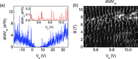
Let us continue the analysis by considering the transport measurements at lower temperature ( mK). In the vicinity of the Dirac point, the conductance measurement versus at zero magnetic field clearly shows a transport gap in a gate-range of V (Fig. 2a). This corresponds to an energy scale of meV, which can be attributed to the disorder-induced potential fluctuations in the ribbon 10-HAN_10-OOS , possibly in conjunction with a lateral confinement gap 09-STA_09-TOD_10-GAL . Earlier transport experiments have shown that, in this low-density regime, electrons are confined in small areas of the ribbon 11-MOL . In our conductance measurements, we clearly observe conductance peaks in the transport gap (inset of Fig. 2a), showing that electron states are indeed localized in the low-density regime and transport is dominated by charging effects. By measuring the conductance as function of magnetic field in a small gate-voltage range of the transport gap (Fig. 2b), we observe conductance peaks in the full magnetic field range, including the quantum Hall regime ( T). This result shows that electrons are confined at low densities, even when the zero-energy LL appears at the Dirac point. This rules out that a bandgap due to lateral confinement plays a crucial role in the physical mechanism underlying the occurrence of the transport gap at high magnetic field (consistent with EdgeDisorder_Theory ; 10-HAN_10-OOS ), because the zero-energy LL closes such a size quantization gap Note4 .
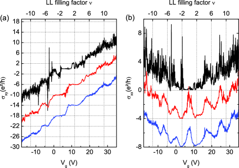
At mK, we observe large reproducible fluctuations of and at high charge densities in the quantum Hall regime (Fig. 3a,b), which obscure the visibility of SdH oscillations of and quantization plateaux of . The transport gap gives rise to a strongly suppressed conductivity tensor in the low-density regime ( if ; see Note2 ). Fig. 3a,b show that the transport gap disappears when we apply a sufficiently high bias, leading to non-vanishing values of and in the vicinity of the Dirac point. Moreover, in the high density regime, the fluctuations of and are suppressed at high bias, and the SdH oscillations of and the quantization plateaux of are more visible.
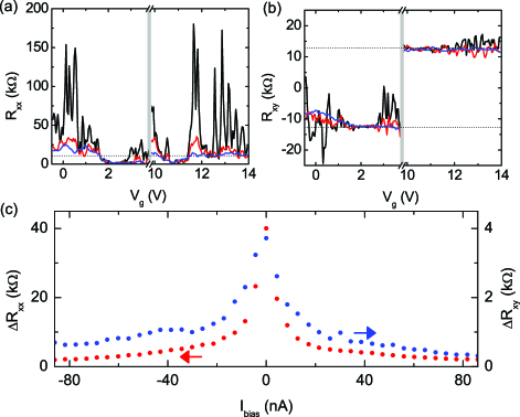
In order to investigate the origin of the reproducible fluctuations at low temperature, we analyze the fluctuations of and in the region of the Hall plateaux (since these are the best developed plateaux in our measurements). Fig. 4a,b show that the fluctuations (, ) are smallest in the center region of the plateaux, whereas they increase strongly farther from the center region (i.e. in the transition regions between adjacent plateaux). The bias-dependence of and (Fig. 4a-c) shows that the fluctuations in the transition regions are strongly suppressed at nA (this corresponds to V, because k in the transition regions; see dotted line in Fig. 4a).
Resistance fluctuations in the quantum Hall regime have been studied extensively in mesoscopic devices based on Si and GaAs heterostructures QHEfluctuations_exp . When the device dimensions are of the order of , phase coherent scattering mechanisms give rise to resistance fluctuations in the quantum Hall regime, similar to universal conductance fluctuations in the zero-field regime 91-BEE_92-BUE . Since our nanoribbon dimensions are of the order of , the observed resistance fluctuations may originate from quantum interference. Fig. 4c shows indeed that the fluctuations are suppressed on an energy scale of 100 eV, which is of the same order as the Thouless energy of the ribbon ( eV). This also explains why these fluctuations are suppressed at 4.2 K, when . Thus, our results indicate that the observed fluctuations in the quantum Hall regime can be mainly attributed to phase coherent scattering mechanisms in the disordered graphene nanoribbon.
In conclusion, we have measured the quantum Hall effect in a 60 nm wide graphene nanoribbon, which results in the observation of SdH oscillations of and quantized plateaux of for , and . At mK, we observe large fluctuations of and at high charge densities, which may be attributed to phase coherent scattering mechanisms in the ribbon. At low charge densities, the electrons are confined in the ribbon yielding a transport gap, in which transport is dominated by charging effects. Since the transport gap does not disappear in the quantum Hall regime, a bandgap due to lateral confinement cannot play a crucial role in the occurrence of the transport gap at high magnetic field (which confirms what has been reported before EdgeDisorder_Theory ; 10-HAN_10-OOS ).
Acknowledgements.
We thank H. Hettmansperger, J. Schelter and B. Trauzettel for useful discussions. This work was financially supported by the German research foundation DFG [DFG-JST joint research program ’Topological Electronics’], and the EU ECR Eurocores programme [Eurographene project].References
- (1) K. S. Novoselov et al., Nature 438, 197 (2005); Y. Zhang, Y. W. Tan, H. L. Stormer & P. Kim, Nature 438, 201 (2005)
- (2) F. Molitor et al., J. Phys.: Condens. Matter. 23, 243201 (2011)
- (3) K. Nakada, M. Fujita, G. Dresselhaus & M. S. Dresselhaus, Phys. Rev. B 54, 17954 (1996); L. Brey & H. A. Fertig, Phys. Rev. B 73, 235411 (2006); Y. W. Son, M. L. Cohen & S. G. Louie, Phys. Rev. Lett. 97, 216803 (2006)
- (4) M. Fujita, K. Wakabayashi, K. Nakada & K. Kusakabe, J. Phys. Soc. Jap. 65, 1920 (1996); Y. W. Son, M. L. Cohen & S. G. Louie, Nature 444, 347 (2006), A. Rycerz, J. Tworzydlo & C. W. J. Beenakker, Nat. Phys. 3, 172 (2007); B. Trauzettel, D. V. Bulaev, D. Loss & G. Burkard, Nat. Phys. 3, 192 (2007)
- (5) D. Gunlycke, D. A. Areshkin & C. T. White, Appl. Phys. Lett. 90, 142104 (2007); A. Lherbier, B. Biel, Y. M. Niquet & S. Roche, Phys. Rev. Lett. 100, 036803 (2008); M. Evaldsson, I. V. Zozoulenko, H. Xu & T. Heinzel, Phys. Rev. B 78, 161407 (2008); D. Querlioz et al., Appl. Phys. Lett. 92, 042108 (2008); E. R. Mucciolo, A. H. Castro Neto & C. H. Lewenkopf, Phys. Rev. B 79, 075407 (2009); I. Martin & Y. M. Blanter, Phys. Rev. B 79, 235132 (2009)
- (6) M. Y. Han, J. C. Brant & P. Kim, Phys. Rev. Lett. 104, 056801 (2010); J. B. Oostinga, B. Sacépé, M. F. Craciun & A. F. Morpurgo, Phys. Rev. B 81, 193408 (2010)
- (7) C. Stampfer et al., Phys. Rev. Lett. 102, 056403 (2009); K. Todd, H. T. Chou, S. Amasha & D. Goldhaber-Gordon, Nano Lett. 9, 416 (2009); P. Gallagher, K. Todd & D. Goldhaber-Gordon, Phys. Rev. B 81, 115409 (2010)
- (8) N. M. R. Peres, A. H. Castro & F. Guinea, Phys. Rev. B 73, 195411 (2006); L. Brey & H. A. Fertig, Phys. Rev. B 73, 195408 (2006)
- (9) Y. M. Lin, V. Perebeinos, Z. Chen & P. Avouris, Phys. Rev. B 78, 161409 (2008); C. Lian et al., Appl. Phys. Lett. 96, 103109 (2010); N. Tombros et al., Nat. Phys. 7, 697 (2011)
- (10) R. Ribeiro et al., Phys. Rev. Lett 107, 086601 (2011); S. Minke et al., Phys. Rev. B 85, 195432 (2012); H. Hettmansperger et al., arXiv:1205.5144 (2012)
- (11) The value of is obtained from Hall measurements at different . The gate-dependence of the Hall coefficient is , resulting in F/m2.
- (12) A. F. Morpurgo & F. Guinea, Phys. Rev. Lett. 97, 196804 (2006); F. V. Tikhonenko, D. W. Horsell, R. V. Gorbachev & A. K. Savchenko, Phys. Rev. Lett. 100, 056802 (2008)
- (13) First the longitudinal magnetoresistance data is symmetrized, , and the Hall data is antisymmetrized, . Then the conductivity tensor values are determined: and with and .
- (14) E. McCann et al., Phys. Rev. Lett. 97, 146805 (2006)
- (15) The LL energy sequence of Dirac fermions in graphene is 05-NOV_05-ZHA : sgn with , , , . The , and plateaux occur when the , and LLs are near complete filling, respectively (note that positive/negative indices account for electron/hole states). Thus, at T, the LL spacings corresponding to the 2, 6, 10 plateaux are 117 meV, 49 meV and 37 meV, respectively.
- (16) The zero-energy LL () of graphene consists of electron and hole states 05-NOV_05-ZHA . This LL therefore closes a bandgap between electron and hole states, which may be present due to lateral confinement. If a size quantization gap would play a crucial role in the electron localization mechanism of our ribbons, then the electrons would delocalize when this gap is closed at high magnetic field.
- (17) P. C. Main et al., Phys. Rev. B 50, 4450 (1994); D. H. Cobden, C. H. W. Barnes & C. J. B. Ford, Phys. Rev. Lett. 82, 4695 (1999); T. Machida, S. Ishizuka, S. Komiyama, K. Muraki & Y. Hirayama, Phys. Rev. B 63, 045318 (2001); F. Hohls, U. Zeitler & R. J. Haug, Phys. Rev. B 66, 073304 (2002); E. Peled, D. Shahar, Y. Chen, D. L. Sivco & A. Y. Cho, Phys. Rev. Lett. 90, 246802 (2003)
- (18) C. W. J. Beenakker & H. van Houten, Solid State Phys. 44, 1 (1991); M. Büttiker, Semicond. Semimetals 35, 191 (1992)