High pressure effect on structure, electronic structure and thermoelectric properties of MoS2
Abstract
We systematically study the effect of high pressure on the structure, electronic structure and transport properties of 2H-MoS2, based on first-principles density functional calculations and the Boltzmann transport theory. Our calculation shows a vanishing anisotropy in the rate of structural change at around 25 GPa, in agreement with the experimental data. A conversion from van der Waals(vdW) to covalent-like bonding is seen. Concurrently, a transition from semiconductor to metal occurs at 25 GPa from band structure calculation. Our transport calculations also find pressure-enhanced electrical conductivities and significant values of the thermoelectric figure of merit over a wide temperature range. Our study supplies a new route to improve the thermoelectric performance of MoS2 and of other transition metal dichalcogenides by applying hydrostatic pressure.
pacs:
31.15.A-, 81.40.Vw, 73.50.Lw, 72.80.GaI Introduction
Molybdenite, MoS2, a typical member of the transition-metal chalcogenide family, consists of alternating sandwiched sub-layers bonded by van der Waals (vdW) interaction. This weak inter-layer interaction, which has rendered it a good solid lubricant Martin et al. (1993), proves also essential in determining the effect of the number of stacking layers on manifold novel properties, such as Raman frequency Lee et al. (2010); Molina-Sánchez and Wirtz (2011); Cheng et al. (2012), band-gap type (direct, indirect) and band-gap size Han et al. (2011); Klein et al. (2001).
Van der Waals interaction may enhance some intriguing properties on one hand, while suppressing electrical transport properties Mansfield and Salam (1953); Thakurta and Dutta (1983); Agarwal and Talele (1986); Kim et al. (2010) on the other. MoS2 and other transition metal dichalcogenide materials were reported to have very pronounced values of thermopower, but poor electrical conductivity Mansfield and Salam (1953); Thakurta and Dutta (1983); Agarwal and Talele (1986); Kim et al. (2010), leading to a negligibly small value of the dimensionless thermoelectric figure of merit (ZT 0.006 at the optimal doping and working temperature) Guo et al. (2012). To improve upon its electrical conductivity for a better value of ZT, pressure/stress may be employed to tune the inter-layer interaction and expected to suppress vdW bonding or to convert it to covalent or metallic type. Encouragingly, similar studies have already been performed on the single layer. Stress-induced enhancement of electron mobility in MoS2 single layer has been demonstrated in experiment Radisavljevic et al. (2011) for a promising nano-electronic device. First-principles calculations have shown that both compressive Yun et al. (2012) and tensile strain Scalise et al. (2012) in a single layer give rise to a reduced band gap. A semiconductor-metal transition was obtained for a compressive strain of about 15 for single-layer MoS2 Scalise et al. (2012). For bulk transition-metal chalcogenide, except for some experimental studies on pressure-induced structural changeAksoy et al. (2006, 2008); Selvi et al. (2006, 2008), there have been so far no theoretical reports on the pressure effect. In particular, how pressure affects the electronic structure and if it can ultimately improve its thermoelectric properties have never been investigated.
In this work, combining first-principles density functional calculations with semiclassical Boltzmann transport theory, we study the change of unit cell allowed by the crystal structure, electronic structure and thermoelectric transport properties of MoS2 under hydrostatic pressure. Our calculation shows a vanishing anisotropy in the rate of structural change at around 25 GPa, in agreement with the experimental data Aksoy et al. (2006). We also find a concurrent conversion from vdW interaction to covalent-like type and a semiconductor-metal transition at about 25 GPa. This transition improves greatly the inter-layer electrical conductivity but still keeps a large value of thermopower (), therefore giving rise to appreciably enhanced thermoelectric transport properties. Values of figure of merit (ZT) as high as 0.65 along cross-plane direction are obtainable in a wide range of temperature (from 200 K to 700 K). Our study demonstrates that applying high hydrostatic pressure can be an effective way to improve the thermoelectric performance of MoS2 and of other transition-metal dichalcogenides.
II Methodology
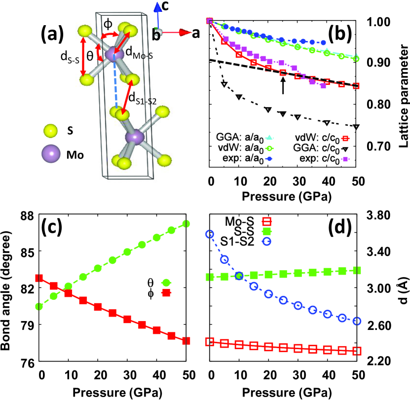
MoS2 has P63/mmc space group symmetry and consists of a hexagonal plane of Mo atoms sandwiched by two hexagonal planes of S atoms. The unit cell contains two alternating layers with an AB stacking along the c axis, as illustrated in Fig. 1(a).
We carried out first-principles calculations based on density functional theory as implemented in the VASP (Vienna ab-initio simulation package)Kresse and Furthmller (1996); Kresse and Joubert (1999) within the framework of the PAW (projector augmented wave) methodBlöchl (1994). The electronic exchange-correlation is described within the generalized gradient approximation (GGA) of Perdew-Burke-Ernzerhof (PBE) flavorPerdew et al. (1996). The vdW corrections Grimme (2006); Dion et al. (2004) are included to determine the inter-layer spacing in 2H-MoS2 and compared to the calculations without vdW corrections. A plane-wave basis set with kinetic energy cutoff of 450 eV is used. For Brillouin-zone(BZ) integrations, We use 424210 k mesh in the full BZ. The unit cell volume, shape and internal atomic positions are optimized under each hydrostatic pressure by using the conjugate gradient method, till the internal atomic force is less than 10-2 eV/ and three diagonal terms in the stress matrix are equal. The convergence for energy is chosen as 10-7 eV between two consecutive steps. We consider the external hydrostatic pressure no larger than 50 GPa, where no occurrence of structural phase transition has been observed experimentally Aksoy et al. (2006) and the structure remains to have P63/mmc space group symmetry.
Transport properties were calculated based on the Boltzmann transport theory applied to the band structure. The integration is done within the BOLTZTRAP transport code Madsen et al. (2003). A very dense mesh with up to 18000 k points in the BZ is used. The electron scattering time is assumed to be independent of energy, an approximation proved to give a good description of thermopower in a number of thermoelectric materials Ong et al. (2011); Parker et al. (2011); Zhang and Singh (2009).
III Results and discussion
We first studied pressure effect on structure of MoS2 and understand the discontinuous structural variation observed in experiment Aksoy et al. (2006). The experimental results, given in Fig.1(b) by filled circles and squares, show that below 25 GPa the rate of reduction of lattice parameters with pressure is different along in-plane and cross-plane directions: c/c0 shrinks much faster than a/a0. This anisotropy vanishes above 25 GPa. We optimized structures both with and without a consideration of the inter-layer van der Waals interaction. The calculated in-plane lattice parameters from both methods are similar and agree with experimental data, while the inter-layer parameters depend on the method. The vdW correction seems essential to account for the experiment. With vdW correction, we also calculated internal structural parameters, including bond angles and bond lengths. As shown in Fig. 1(c,d), the intra-layer parameters (the S-Mo-S bond angles , and the bond lengths dMo-S, dS-S) change very little compared to the inter-layer dS1-S2(the distance between sulfur ions in adjacent layers). dS1-S2, presented in Fig. 1(d), shrinks abruptly with pressure especially below 25 GPa. This indicates that a substantial pressure induces a change of inter-layer interaction.
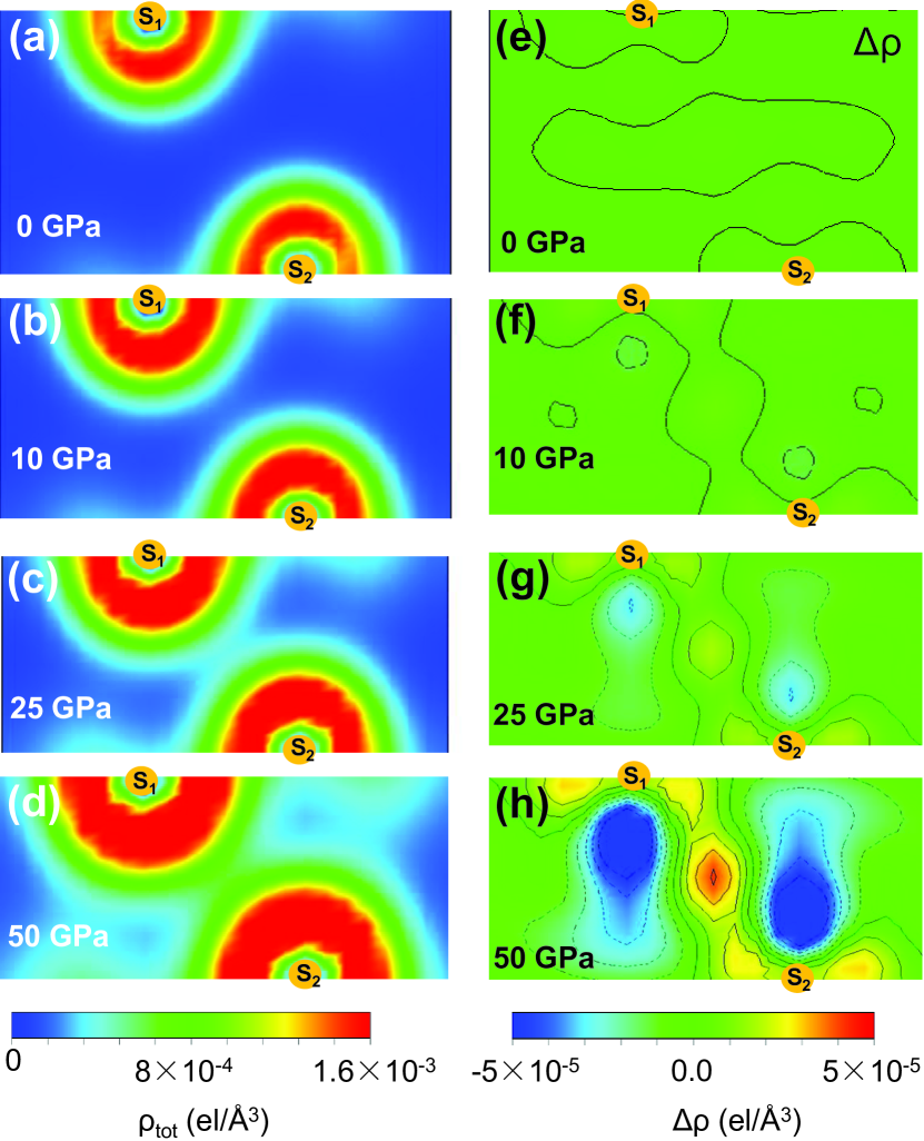
To see what happens to the inter-layer interaction upon pressure, we studied total charge densities in the region between S1 and S2 atom under hydrostatic pressure ranging from 0 to 50 GPa (Fig. 2). Compared to no charge distribution between two neighboring layers at 0 and 10 GPa in Fig. 2(a, b), electron charge becomes more and more converged as illustrated from Fig. 2(c) to (d). As d is decreasing with pressure, the vdW interaction seems firstly to increase, due to both nonspherical-charge-distribution-induced electric dipole on S1 and S2 atom (Fig.2(a) and (b)) and reduced atomic distance by pressure. This trend is consistent with that in ultra-thin MoS2 (few-layers)Cheng et al. (2012). Then a weak covalent-like bond starts to form at 25 GPa and grows stronger at 50 GPa. To support this view, we also studied charge transfer between AB-stacking charge density (AB) and the sum of the two independent densities ((A) + (B)) of A and B sub-layers. There is charge transfer induced by pressure and charge accumulates mostly between S1 and S2 atoms.
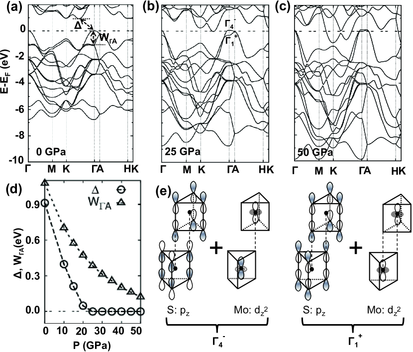
The change of inter-layer interaction will naturally lead to dependence of band structure on pressure. Fig. 3 gives the calculated band structure evolving with pressure from 0 to 50 GPa. Fermi energies of semiconductors are set at valence band maximum (VBM). The behavior of the band gap is shown from (a) to (c) and summarized in (d). At zero pressure the indirect band gap is between VBM at the point and conduction band minimum (CBM) between and K points. Applied pressure causes the CBM to drop, decreases monotonically with pressure till a semiconductor-metal transition occurs at 25 GPa. This only takes an in-plane compressive strain of 5.5%, in contrast to 15% in single layer Scalise et al. (2012). It seems much easier for the bulk material than the single layer to close the band gap by applying pressure, presumably due to the existing inter-layer interaction.
It is worth noting that an increase of band dispersion with pressure is observed, except for two bands near the Fermi level, between the and A points. These two bands are actually zone-folded from one band as the unit cell has one sub-layer. For convenience, both bands are treated as one with band width WΓA, as defined in Fig. 3(a). From Fig. 3(d), WΓA decreases from 1.1 eV (at 0 GPa) via 0.39 eV (at 25 GPa) to 0.12 eV (at 50 GPa). To understand the counterintuitive behavior of the band dispersion decreasing with pressure, we look into the Mo-d and S-p orbitals close to the Fermi level, since they play predominate roles in forming conduction channels for both in-plane and cross-plane directionsMattheiss (1973). The two cross-plane bands with the anomalous width WΓA are due to hybridization of Mo-d (or d for simplicity) and S-pz orbitals. The symmetries of possible combinations of Mo-d and S-pz orbitals are illustrated in Fig. 3(e). The VBM at point has a symmetry Klein et al. (2001); Mattheiss (1973); gam (a), and the band below has a dominating contribution of S-pz orbitals with symmetry Mattheiss (1973); gam (b). We found the valence band have S-pz anti-bonding characteristic. In this sense, the shrinkage of inter-layer distance dS1-S2 with pressure suggests a stronger anti-bonding state and therefore a narrower band dispersion near EF from to A.
From the band structures shown above, we can extract some useful information on the electrical conductivity of the metallic states of MoS2. In Fig. 3(b,c), we found the Fermi velocity (vF) and effective mass (m∗) respectively increasing and decreasing with pressure. Calculated electronic densities of states (DOSs) (not shown here) of the Fermi level at 25 and 50 GPa are 0.19 and 0.53 electrons/eV/u.c., respectively. Under thermal excitation within a range of interest (e.g., 100-700 K, equivalent to 0.009-0.060 eV of energy), DOSs translate to carrier concentrations of approximately 1.51020 and 51020 cm-3 for 25 and 50 GPa, respectively. The boost of carrier concentration by pressure, together with increased vF and reduced m∗, suggest pressure-enhanced electrical conductivity. For semiconducting states below 25 GPa, pressure reduces the band gap size, which helps improve the electrical conductivity but very little. Electron/hole doping Mansfield and Salam (1953) was used but it turns out to be quite challenging to dope in bulk MoS2. So far the highest experimental doping level on MoS2 has reached only a few 1016 cm-3, far below 1019 cm-3 usually for optimizing the thermoelectric performance of semiconducting materials Ong et al. (2011); Guo et al. (2012).
Information on thermopower can also be extracted from the band structures. According to the Mott relation Cutler and Mott (1969), thermopower depends crucially on the derivative of the logarithmic electrical conductivity at the Fermi level Ziman (1995); Ong et al. (2010), i.e., S . Based upon this formula, a strong thermopower is anticipated for both in-plane and cross-plane directions at 25 GPa. Moreover, the anomalous -A bands upon pressure get more flat due to inter-layer anti-bonding states existing and its band edges locate near the Fermi level. It is therefore more advantageous for having high values of thermopower along cross-plane direction as pressure goes beyond 25 GPa.
We have discussed qualitatively how the effect of pressure on thermopower and electrical conductivity can be estimated from some aspects of the band structure. Now we turn to semi-classical Boltzmann transport theory for quantitative prediction on the thermoelectric parameters of MoS2 under pressure.
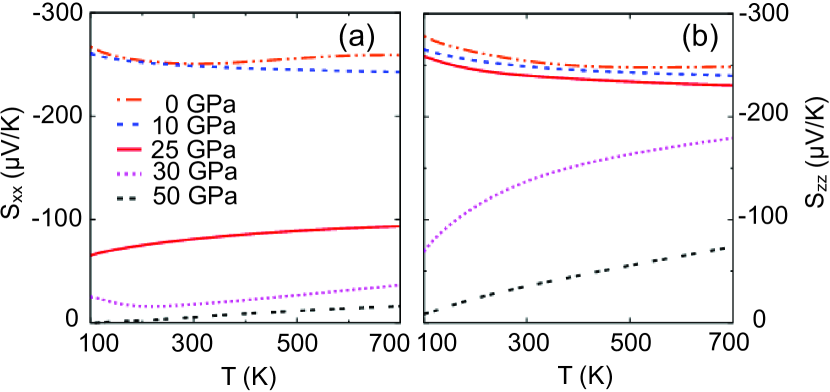
Firstly, we calculated thermopower as function of temperature at 0, 10, 25, 30 and 50 GPa. From Fig. 4, a strong anisotropy of the thermopower between two perpendicular directions appears when pressure increases from 0 to 25 GPa. The in-plane thermopower Sxx drops substantially while the cross-plane thermopower Szz goes down fairly modestly. The Sxx at pressure above 25 GPa is as low as in typical metalsBlatt et al. (1976). In the contrary, high values of the Seebeck coefficient Szz were indeed obtained along cross plane direction. Especially, over 100 V/K along c-axis are achievable over a wide temperature range above 25 GPa. Least important to mention is that a big value of thermopower is also found for the semiconducting MoS2 at 0 and 10 GPa (with experimental doping 1016 cm-3), which is however not very unusual from theoretical perspective Mahan (1998).
Similarly, we then calculated / as a function of temperature. Our results show that / increases with external pressure. So does the electrical conductivity , if is approximately pressure independent. To find a realistic temperature dependence of without available experimental , we assume that at high temperature the conduction electrons are mainly scattered by phonons and the electronic relaxation time T-1 is used Ziman (1995, 2001). Hence /(T) as function of temperature can give information on temperature dependence of . We show in-plane and cross-plane /(T) versus temperature in Fig.5(a,b). For both directions, typical metallic behavior is seen by an inverse power law relation between /(T) and temperature at pressure higher than 25 GPa, while below 25 GPa it is semiconducting. At 25 GPa, a deviation from the inverse power law is observed and suggests its conductive properties different from typical metals and semiconductors.
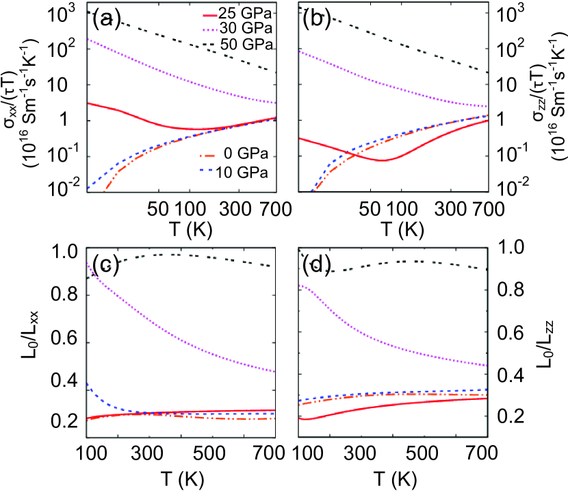
As is known, the dimensionless thermoelectric figure of merit ZT is defined as (or ), with (= + ), and as total, electronic and lattice thermal conductivity, respectively, L = and = . To evaluate a possible enhancement of ZT value by external pressure, we need to calculate the pressure dependence of thermal conductivity . Unfortunately, calculating lattice thermal conductivity is far more complicated than calculating and it is beyond band structure calculations. Here we argue that can substitute for under various pressures if MoS2 becomes metallic, since is insignificant compared to in most metalskap . For a typical metal, the Wiedemann-Franz law works and L is a constant called Lorenz number L0(= 2.8 10-8 W/K2). In Fig. 5(c,d), we draw a ratio of L0 over L as function of temperature at various pressures. The ratio L0/L approaches unity as pressure increases from 25 to 50 GPa, indicating an evaluation of ZT value based on is legitimate. However, a strong deviation from the Wiedemann-Franz law occurs to the semiconducting states below and at 25 GPa, signifying may be as important as or even more significant than .
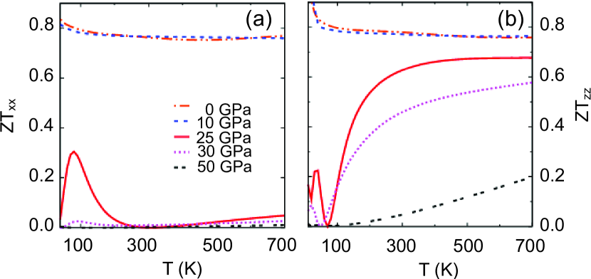
Assuming ZT is approximately and bearing in mind that it may not work for semiconducting states even with heavy doping, we show the calculated ZT value in Fig. 6. Though ZT values for semiconducting MoS2 at 0 and 10 GPa seem practically high, it is basically unreliable since the can be orders of magnitude higher than and brings down ZT by similar orders of magnitudeGuo et al. (2012). At transitional 25 GPa, ZT can reach 0.05 in plane and 0.65 along the c axis over a wide range of temperature. But due to the uncertainty between and this may need experimental confirm. What’s promising here is that the values of cross-plane ZT decrease modestly as pressure goes beyond 25 GPa. Still significant ZT value higher than 0.10 is obtained over a wide range of pressure, suggesting that a proper range of pressure is essential to optimize the thermoelectric properties of MoS2.
IV Conclusion
In summary, we systematically studied the structure, electronic structure and transport properties of 2H-MoS2 under hydrostatic pressure, based on the Boltzmann transport theory and first-principles density functional calculations. VdW corrections to GGA calculations are essential to deal with such an anisotropic system under pressure. Our calculation shows a vanishing anisotropy in the rate of structural change at around 25 GPa, in agreement with the experimental data. A conversion from vdW to covalent-like bonding is seen. Concurrently, a transition from semiconductor to metal occurs at 25 GPa. A much smaller compressive strain in bulk material than in single layer is needed to close the band gap. We obtained in the metallic state very large values of the thermopower and ascribed it to some anomalous band features. Above all, good values of figure of merit are found along the cross-plane direction. The ZT value can be obtained as big as 0.10 (even up to 0.65) over a wide pressure and temperature range. Our study supplies a new route to improve the thermoelectric performance of MoS2 and of other transition metal dichalcogenides by applying hydrostatic pressure.
Acknowledgements.
The authors thank Dr. Peter F. de Chtel for useful discussions. This work was supported by the NSFC under Grant No. 11004201, 50831006 and the National Basic Research Program (No. 2012CB933103). T.Y. acknowledges IMR SYNL Young Merit Scholars and T.S. K Research Grant for support.References
- Martin et al. (1993) J. M. Martin, C. Donnet, Th. Le Mogne, and Th. Epicier, Phys. Rev. B 48, 10583 (1993).
- Lee et al. (2010) C. Lee, H. Yan, L. E. Brus, T. F. Heinz, J. Hone, and S. Ryu, ACS Nano 4, 2695 (2010).
- Molina-Sánchez and Wirtz (2011) A. Molina-Sánchez and L. Wirtz, Phys. Rev. B 84, 155413 (2011).
- Cheng et al. (2012) Y. Cheng, Z. Zhu, and U. Schwingenschlgl, RSC Advances 2, 7798 (2012).
- Han et al. (2011) S. W. Han, H. Kwon, S. K. Kim, S. Ryu, W. S. Yun, D. H. Kim, J. H. Hwang, J.-S. Kang, J. Baik, H. J. Shin, et al., Phys. Rev. B 84, 045409 (2011).
- Klein et al. (2001) A. Klein, S. Tiefenbacher, V. Eyert, C. Pettenkofer, and W. Jaegermann, Phys. Rev. B 64, 205416 (2001).
- Mansfield and Salam (1953) R. Mansfield and S. A. Salam, Proc. Phys. Soc. B 66, 377 (1953).
- Thakurta and Dutta (1983) S. G. Thakurta and A. Dutta, J. Phys. Chem. Solids 44, 407 (1983).
- Agarwal and Talele (1986) M. Agarwal and L. Talele, Solid State Commun. 59, 549 (1986).
- Kim et al. (2010) J.-Y. Kim, S. M. Choi, W.-S. Seo, and W.-S. Cho, Bull. Korean Chem. Soc. 31, 3225 (2010).
- Guo et al. (2012) H. H. Guo, T. Yang, P. Tao, and Z. D. Zhang, submitted (2012).
- Radisavljevic et al. (2011) B. Radisavljevic, A. Radenovic, J. Brivio, V. Giacometti, and A. Kis, Nature Nanotechnology 6, 147 (2011).
- Yun et al. (2012) W. S. Yun, S. W. Han, S. C. Hong, I. G. Kim, and J. D. Lee, Phys. Rev. B 85, 033305 (2012).
- Scalise et al. (2012) E. Scalise, M. Houssa, G. Pourtois, V. Afanas′ev, and A. Stesmans, Nano Res. 5, 43 (2012).
- Aksoy et al. (2006) R. Aksoy, Y. Ma, E. Selvi, M. C. Chyu, A. Ertas, and A. White, J. Phys. Chem. Solids 67, 1914 (2006).
- Aksoy et al. (2008) R. Aksoy, E. Selvi, and Y. Ma, J. Phys. Chem. Solids 69, 2138 (2008).
- Selvi et al. (2006) E. Selvi, Y. Ma, R. Aksoy, A. Ertas, and A. White, J. Phys. Chem. Solids 67, 2183 (2006).
- Selvi et al. (2008) E. Selvi, R. Aksoy, R. Knudson, and Y. Ma, J. Phys. Chem. Solids 69, 2311 (2008).
- Kresse and Furthmller (1996) G. Kresse and J. Furthmller, Phys. Rev. B 54, 11169 (1996).
- Kresse and Joubert (1999) G. Kresse and D. Joubert, Phys. Rev. B 59, 1758 (1999).
- Blöchl (1994) P. E. Blöchl, Phys. Rev. B 50, 17953 (1994).
- Perdew et al. (1996) J. P. Perdew, K. Burke, and M. Ernzerhof, Phys. Rev. Lett. 77, 3865 (1996).
- Grimme (2006) S. Grimme, J. Comput. Chem. 27, 1787 (2006).
- Dion et al. (2004) M. Dion, H. Rydberg, E. Schröder, D. C. Langreth, and B. I. Lundqvist, Phys. Rev. Lett. 92, 246401 (2004).
- Madsen et al. (2003) G. K. H. Madsen, K. Schwarz, P. Blaha, and D. J. Singh, Phys. Rev. B 68, 125212 (2003).
- Ong et al. (2011) K. P. Ong, D. J. Singh, and P. Wu, Phys. Rev. B 83, 115110 (2011).
- Parker et al. (2011) D. Parker, M.-H. Du, and D. J. Singh, Phys. Rev. B 83, 245111 (2011).
- Zhang and Singh (2009) L. Zhang and D. J. Singh, Phys. Rev. B 80, 075117 (2009).
- Mattheiss (1973) L. F. Mattheiss, Phys. Rev. B 8, 3719 (1973).
- gam (a) symmetry: antisymmetric electronic states from two MoS2 sub-layers with respect to inversion, symmetric with respect to horizontal mirror plane within one sub-layer.
- gam (b) symmetry: symmetric electronic states from two MoS2 sub-layers with respect to inversion, symmetric with respect to horizontal mirror plane within one sub-layer.
- Cutler and Mott (1969) M. Cutler and N. F. Mott, Phys. Rev. 181, 1336 (1969).
- Ziman (1995) J. M. Ziman, Principles of the theory of solids, 2nd Ed. (Cambridge University Press, 1995).
- Ong et al. (2010) K. P. Ong, D. J. Singh, and P. Wu, Phys. Rev. Lett. 104, 176601 (2010).
- Blatt et al. (1976) F. J. Blatt, P. A. Schroeder, C. L. Foiles, and D. Greig, Thermoelectric Power of Metals (Plenum Press, 1976).
- Mahan (1998) G. D. Mahan, Solid State Physics, vol. 51, ed. by H. Ehrenreich and F. Spaepen (Academic Press, 1998).
- Ziman (2001) J. M. Ziman, Electrons and phonons (Clarendon Press, 2001).
- (38) The thermal conductivity is insignificant compared to in metallic states, due to the following reasons:(1) At low T, dominates in the metals. (2) At high T, is temperature-insensitive under circumstance of T-1, while decreases with temperature, as experiments suggested Kim et al. (2010). It makes even more insignificant than . (3) It would reduce our estimation of ZT by only one half if were comparable to .