Josephson -junctions based on structures with complex normal/ferromagnet bilayer
Abstract
We demonstrate that Josephson devices with nontrivial phase difference in the ground state can be realized in structures composed from longitudinally oriented normal metal (N) and ferromagnet (F) films in the weak link region. Oscillatory coupling across F-layer makes the first harmonic in the current-phase relation relatively small, while coupling across N-layer provides negative sign of the second harmonic. To derive quantitative criteria for a -junction, we have solved two-dimensional boundary-value problem in the frame of Usadel equations for overlap and ramp geometries of S-NF-S structures. Our numerical estimates show that -junctions can be fabricated using up-to-date technology.
pacs:
74.45.+c, 74.50.+r, 74.78.Fk, 85.25.CpI Introduction
The relation between supercurrent across a Josephson junction and phase difference between the phases of the order parameters of superconducting (S) banks is an important characteristic of a Josephson structure Likharev ; RevG . In standard SIS structures with tunnel type of conductivity of a weak link, the current-phase relation (CPR) has the sinusoidal form . On the other hand, in SNS or SINIS junctions with metallic type of conductivity the smaller the temperature the larger the deviations from the form Likharev and achieves its maximum at . In SIS junctions the amplitude of second harmonic in CPR, is of the second order in transmission coefficient of the tunnel barrier I and therefore is negligibly small for all . In SNS structures the second CPR harmonic is also small in the vicinity of critical temperature of superconductors, where . At low temperatures , the coefficients and have comparable magnitudes, thus giving rise to qualitative modifications of CPR shape with decrease of
It is important to note that in all types of junctions discussed above the ground state is achieved at , since at a junction is at nonequilibrium state.
The situation changes in Josephson structures involving ferromagnets as weak link materials. The possibility of the so-called “-state” in SFS Josephson junctions (characterized by the negative sign of the critical current ) was predicted theoretically and observed experimentally [RevG, -AnwarLR, ]. Contrary to traditional Josephson structures, in SFS devices it is possible to have the ground state (so-called -junctions), while the corresponds to an unstable situation. It was proven experimentally Rogalla ; Feofanov that -junctions can be used as on-chip -phase shifters or -batteries for self-biasing various electronic quantum and classical circuits. It was proposed to use self -biasing to decouple quantum circuits from environment or to replace conventional inductance and strongly reduce the size of an elementary cell Ustinov .
In some classical and quantum Josephson circuits it is even more interesting to create on-chip -batteries. They are -junctions, the structures having phase difference , between superconducting electrodes in the ground state. The -states were first predicted by MintsMints for the case of randomly distributed alternating and Josephson junctions along grain boundaries in high cuprates with d-wave order parameter symmetry. It was shown later that -junctions can be also realized in the periodic array of and SFS junctions Buzdin ; Pugach . It was demonstrated that depending on the length of or segments in the array, a modulated state with the average phase difference can be generated if the mismatch length between the segments is small. This can take any value within the interval . Despite strong constraints on parameter spread of individual segments estimated in SPIE , remarkable progress was recently achieved on realization of -junctions in such arrays Gold .
In general, in order to implement a -junction one has use a Josephson junction having non-sinusoidal current-phase relation, which, at least, can be described by a sum of two terms
| (1) |
Moreover, the following special relationship between the amplitudes of the CPR harmonics, and, is needed for existence of equilibrium stable state Gold2007 ; Klenov
| (2) |
In conventional junctions, the magnitude of is larger than that of and the inequalities (2) are difficult to fulfill. However, in SFS junctions in the vicinity of to transition the amplitude of first harmonic in CPR is close to zero, thus opening an opportunity for making a battery, if can be made negative. It is well-known that SFS junctions with metallic type of conductivity, as well as SIFS structures Vasenko ; Vasenko1 with high transparencies of SF interfaces have complex decay length of superconducting correlations induced into F-layer . Unfortunately, the conditions (2) are violated in these types junctions since the , , and for corresponding to the first - transition the second harmonic amplitude is positive.
Quantitative calculations made in the framework of microscopic theoryBuzdin1 ; Vinokur confirm the above qualitative analysis. In Ref. Buzdin1 ; Vinokur it was demonstrated that in SFS sandwiches with either clean or dirty ferromagnetic metal interlayer the transition from to state is of the first order, that is at any transition pointRevB .
It was suggested recently in Karminskaya -Bakurskiy1 to fabricate the ”current in plane” SFS devices having the weak link region consisting from NF or FNF multilayers with the supercurrent flowing parallel to FN interfaces. In these structures, superconductivity is induced from the S banks into the normal (N) film, while F films serves as a source of spin polarized electrons, which diffuse from F to N layer thus providing an effective exchange field in a weak link. Its strength it can be controlledBergeret ; Fominov by transparencies of NF interfaces, as well as by the products of densities of states at the Fermi level, and film thicknesses, . It was shown in Karminskaya -Karminskaya4 that the reduction of effective exchange energy in a weak link permits to increase the decay length from the scale of the order of nm up to nm. The calculations performed in these papers did not go beyond linear approximation in which the amplitude of the second harmonic in the CPR is small. Therefore, the question of the feasibility of contacts in these structures has not been studied and remains open to date.
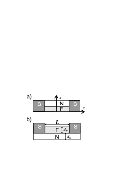
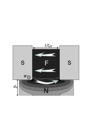
The purpose of this paper is to demonstrate that the same ”current in plane” devices (see Fig. 1) can be used as effective -shifters. The structure of the paper is the following. In Sec.II we present general qualitative discussion of the microscopic mechanisms leading to formation of higher harmonics in the CPR. In Sec.III we formulate quantitative approach in terms of Usadel equations. In Sec IV the criteria of -state existence are derived for ramp-type S-FN-S structure. Section V shows the advantage of the other geometries in order to realize -state. Finally in Sec.VI we consider properties of real materials and estimate the possibility to realize -states using up-to-date technology.
II CPR formation mechanisms
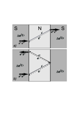
In this section we shall discuss microscopic processes which contribute to formation of CPR in Josephson junctions. The physical reason leading to the sign reversal of the coefficient in SFS junctions compared to that in SNS structures can be understood from simple diagram shown in Fig.2 illustrating the mechanisms of supercurrent transfer in double barrier Josephson junctions.
Consider electron-like quasiparticle propagating across SINIS structure towards the right electrode. This quasiparticle can be reflected either in the Andreev or in the normal channel.
The result of the first process (see Fig.2a) is generation in the weak link region (with an amplitude proportional to ) of the hole propagating in the opposite direction. Andreev reflection of this hole at the second interface (with an amplitude proportional to ) results in transfer of a Cooper pair from the left to the right electrode with the rate proportional to the net coefficient of Andreev reflection processesFurusaki ; Furusaki1 at both SN interfaces, The amplitude, depends on geometry of a structure and on material parameters. Note that for given values of these parameters according to the detailed balance relationsFurusaki . Similar considerations show that a quasiparticle moving towards the left electrode generates a Cooper pair propagating from the right to the left interface with the rate proportional to The difference between two processes described above determines a supercurrent , which is proportional to
The result of the second process is the change (with an amplitude proportional to ) of the propagation direction to the left electrode and nucleation of a Cooper pair and a hole propagating to the right electrode (with an amplitude proportional to ). After normal reflection from the right interface (with an amplitude proportional to ) the hole arrives at the left SN interface and closes this Andreev loop by generating a Cooper pair in the left electrode and an electronic state (with an amplitude proportional to The Cooper pair have to undergo a full reflection at SN interface, thus again a pair is generated moving in the direction opposite to that in the main Andreev loop. The net coefficient of this Andreev reflection process is For a quasiparticle moving in the weak link towards the left electrode the same consideration leads to generation of two Cooper pairs moving from the left to the right with the rate proportional to The difference between these two processes determines a part of supercurrent proportional to
We have shown that supercurrent components proportional to and have opposite signs, and the coefficient in Eq.(1) is negative. This statement is in a full agreement with calculations of the CPR performed in the frame of microscopic theory of superconductivityLikharev ; RevG . It is valid if a supercurrent across a junction does not suppress superconductivity in S electrodes in the vicinity of SN interfacesIvanov ; Zubkov ; KuperD . In addition, an effective path of the particles in the second process discussed above is two times larger than in the first one. This leads to stronger decay of the second harmonic amplitude with increasing the distance .
In SFS junctions the situation becomes more complicated. The exchange field, in the weak link removes the spin degeneracy of quasiparticles. As a result, one has to consider four types of Andreev’s loops instead of two loops discussed above. One should also take into account the fact that wave function of a quasiparticle propagating through the weak link acquires an additional phase shift proportional to the magnitude of the exchange fieldBeasley . The sign of depends on mutual orientations between magnetization of the ferromagnetic film and the spin of a quasiparticle. Taking into account these phase shifts and repeating arguments similar to given above, one can show that the coefficients A and B in Eq.(1) acquire additional factors and respectively. At the point of - transition the coefficient , that is . As a result, provides an additional factor, which changes the sign of the second harmonic amplitude in SFS structures from negative to positive.
In the present study we will show that contrary to SFS devices with standard geometry, it’s possible to realize -junctions in the structures shown in Fig. 1. Qualitatively, these structures are superpositions of parallel SNS and SFS-channels, where supercurrent can be decomposed into two parts, and , flowing across N and F films, respectively. For and at sufficiently low temperatures has large negative second CPR harmonic . For supercurrent in the SFS-channel exhibits damped oscillations as a function of . In this regime the second harmonic of CPR is negligibly small compared to the first one. Large difference between decay lengths of superconducting correlations in N and F-materials allows one to enter the regime when . In this case the first CPR harmonic can be made small enough due to negative sign of while the second CPR harmonic is negative, thus making it possible to fulfill the condition (2). Note that we are considering here the regime of finite interface transparencies, when higher order harmonics decay fast with the harmonic order. Therefore, it is sufficient to consider only the first and the second harmonics of the CPR in all our subsequent discussions.
We show below that the mechanism described above indeed works in the considered S-FN-S junctions, and we estimate corresponding parameter range when states can be realized.
III Model
We consider two types of symmetric multilayered structures shown schematically on Fig.1. The structures consist of a superconducting (S) electrode contacting either the end-wall of a FN bilayer (ramp type junctions) or the surface of F or N films (overlap junction geometry). The FN bilayer consists of ferromagnetic (F) film and normal metal (N) having a thickness , and respectively. We suppose that the conditions of a dirty limit are fulfilled for all metals and that effective electron-phonon coupling constant is zero in F and N films. For simplicity we assume that the parameters and which characterize the transparencies of NS and FS interfaces are large enough
| (3) |
in order to neglect suppression of superconductivity in S parts of the junctions. Here and are the resistances and areas of the SN and SF interfaces, and are the decay lengths of S, N, F materials and and are their resistivities.
Under the above conditions the problem of calculation of the supercurrent in the structures reduces to solution of the set of Usadel equationsRevB ; RevV ; Usadel
| (4) |
where and are Usadel Green’s functions in parametrization. They are and or and in N and F films correspondingly, are Matsubara frequencies (m=0,1,2,…), is exchange field of ferromagnetic material, for N and F layers respectively, are diffusion coefficients, is 2D gradient operator. To write equations (4), we have chosen the and axis in the directions, respectively, perpendicular and parallel to the plane of N film and we have set the origin in the middle of structure at the free interface of F-film (see Fig.1).
The supercurrent can be calculated by integrating the standard expressions for the current density over the junction cross-section:
| (5) |
where is the width of the junctions, which is supposed to be small compared to Josephson penetration depth. It is convenient to perform the integration in (5) in F and N layers separately along the line located at , where -component of supercurrent density vanishes by symmetry.
Eq.(4) must be supplemented by the boundary conditions KL . Since these conditions link the Usadel Green’s functions corresponding to the same Matsubara frequency , we may simplify the notations by omitting the subscript . At the NF interface the boundary conditions have the form:
| (6) |
where and are the resistance and area of the NF interface.
The conditions at free interfaces are
| (7) |
The partial derivatives in (7) are taken in the direction normal to the boundary, so that can be either or depending on the particular geometry of the structure.
In writing the boundary conditions at the interface with a superconductor, we must take into account the fact that in our model we have ignored the suppression of superconductivity in electrodes, so that in superconductor
| (8) |
where is magnitude of the order parameter in S banks. Therefore for NS and FS interfaces we may write:
| (9a) | ||||
| (9b) | ||||
| As in Eq. (7), in Eqs. (9a), (9b) is a normal vector directed into material marked at derivative. | ||||
For the structure presented in Fig.1a, the boundary-value problem (4) - (9b) was solved analytically in the linear approximationKarminskaya3 ; Karminskaya4 , i.e. under conditions
| (10) |
In the present study we will go beyond linear approximation where qualitatively new effects are found.
IV Ramp-type geometry
The ramp type Josephson junction has simplest geometry among the structures shown in Fig.1. It consists of the NF bilayer, laterally connected with superconducting electrodes (see Fig.1a).
In general, there are three characteristic decay lengths in the considered structureKarminskaya ,Karminskaya3 ,Crouzy . They are and The first two lengths determine the decay and oscillations of superconducting correlations far from FN interface, while the last one describes their behavior in its vicinity. Similar length scale occurs in a vicinity of a domain wallChtchelkatchev -Crouzy . In the latter, exchange field is averaged out for antiparallel directions of magnetizations, and the decay length of superconducting correlations becomes close to . At FN interface, the flow of spin-polarized electrons from F to N metal and reverse flow of unpolarized electrons from N to F suppresses the exchange field in its vicinity to a value smaller than that in a bulk ferromagnetic material thus providing the existence of . Under certain set of parametersKarminskaya these lengths, , and, can become comparable to which is typically much larger than and , which are equal to for .
The existence of three decay lengths, and should lead to appearance of three contributions to total supercurrent, and respectively. The main contribution to component comes from a part of the supercurrent uniformly distributed in a normal film. In accordance with the qualitative analysis carried out in Section II, it is the only current component which provides a negative value of the amplitude of the second harmonic in the current-phase relation. The smaller the distance between electrodes , the larger this contribution. To realize a contact, one must compensate for the amplitude of the first harmonic, in a total current to a value that satisfies the requirement (2). Contribution to from also increases with decreasing . Obviously, it’s difficult to suppress the coefficient due to the contribution only, since flows through thin near-boundary layer. Therefore, strong reduction of required to satisfy the inequality (2) can only be achieved as a result of compensation of the currents and flowing in opposite directions in N and F films far from FN interface. Note that the oscillatory nature of the dependence allows to satisfy requirement (2) in a certain range of . The role of in a balance between and can be understood by solving the boundary value problem (4) - (9b) which admits an analytic solution in some limiting cases.
IV.1 Limit of small
Solution of the boundary-value problem (4)-(9b) can be simplified in the limit of small distance between superconducting electrodes
| (11) |
In this case one can neglect non-gradient terms in (4) and obtain that contributions to the total current resulting from the redistribution of currents near the FN interface cancel each other leading to (see Appendix A for the details). As a result, the total current is a sum of two terms only
| (12) |
| (13) |
where . The currents and flow independently across F and N parts of the weak link. The dependencies coincide with those calculated previously for double-barrier junctionsKL in the case when lies within the interval defined by the inequalities (11).
It follows from (12), (13) that in the considered limit neither the presence of a sharp FN boundary in the weak link region, nor strong difference in transparencies of SN and SF interfaces lead to intermixing of the supercurrents flowing in the F and N channels. It is also seen that amplitude of the first harmonic of current component is always positive and the requirement (2) can not be achieved.
IV.2 Limit of intermediate
For intermediate values of spacing between the S electrodes
| (14) |
and for the values of suppression parameters at SN and SF interfaces satisfying the conditions (3), the boundary problem (4)-(9b) can be solved analytically for sufficiently large magnitude of suppression parameter It is shown in Appendix B that under these restrictions in the first approximation we can neglect the suppression of superconductivity in the N film due to proximity with the F layer and find that
| (15) |
while spatial distribution of includes three terms: the first two describe the influence of the N film, while the last one has the form well known for SFS junctions RevG ,RevB ,RevV .
Substitution of these solutions into expression for the supercurrent (5) leads to dependence consisting of three terms
| (16) |
Here is the supercurrent across the N layer. In the considered approximation is given by the expression (12). The second term in (16) equals to supercurrent across SFS double barrier structure in the limit of small transparencies of SF interfacesGolubov1 ,DBbuz
| (17) |
where
IV.3 -state existence
The conditions for the implementation of a contact are the better, the larger the relative amplitude of the second harmonic which increases at low temperatures. Therefore, low temperature regime is most favorable for a state. In the limit we can go from summation to integration over in (12), (17), (74)- (76). From (12) we have
| (19) |
where is the complete elliptic integral of the first kind. Expanding expression (19) in the Fourier series it is easy to obtain
| (20) |
| (21) |
where are the first and the second harmonic amplitudes of ,
where is Gamma-function and is generalized hypergeometric function.
Evaluation of the sums in (17), (74)- (76) can be done for and resulting in with
| (22) |
and Substitution of (20), (21) into the inequalities (2) gives -state requirements for ramp-type structure
| (23) |
This expression gives the limitation on geometrical and materials parameters of the considered structures providing the existence of -junction. Function has the first minimum at . For large values of inequality (23) can not be fulfilled at any length . Thus solutions exist only in the area with upper limit
| (24) |
At the left hand side of inequality (23) equals to its right hand part providing the nucleation of an interval of in which we can expect the formation of a -contact. This interval increases with decrease of and achieves its maximum length
| (25) |
at It is necessary to note that at there is a transformation of the left hand side local minimum in (23), which occurs at into local maximum; so that at the both sides of (23) become equal to each other, and the interval (25) of junction existence subdivides into two parts. With a further decrease of these parts are transformed into narrow bands, which are localized in the vicinity of the transition point ; they take place at and The width of the bands decreases with decrease of
Thus, our analysis has shown that for
| (26) |
we can expect the formation of junction in a sufficiently wide range of distances between the electrodes determined by (23). Now we will take into the account the impact of the interface term . In the considered approximations, it follows from (74)- (76) that
| (27) |
| (28) |
| (29) |
where In the range of distances between the electrodes currents and are negative. These contributions have the same form of CPR as it is for the term, and due to negative sign suppress the magnitude of supercurrent across the junction thus making the inequality (23) easier to perform. The requirement imposes additional restriction on the value of the suppression parameter
| (30) |
In derivation of this inequality we have used the fact that in the range of distances between the electrodes depending on factor in (29) is of the order of unity. It follows from (30) that for a fixed value of domain of -junction existence extends with increase of thickness of normal films and this domain disappears if becomes smaller than the critical value,
| (31) |
The existence of the critical thickness follows from the fact that the amplitude in is proportional to while in term the parameter is independent on The sign of is positive for and negative for thus providing an advantage for a junction realization for the lengths which belong to the second interval.
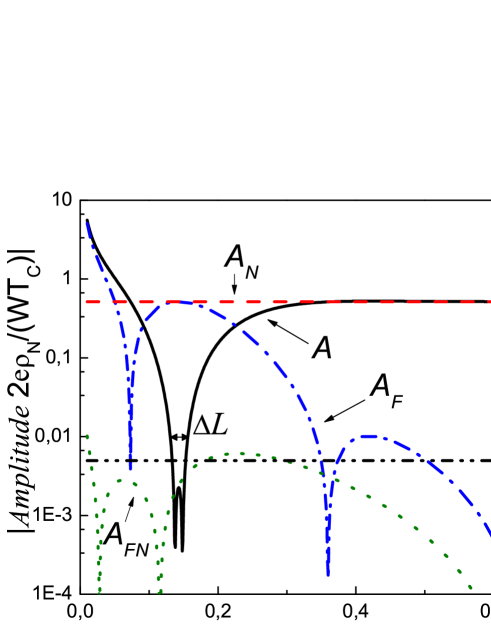
Figure 3 illustrates our analysis. The solid line in Fig.3 is the modulus of the amplitude of the first harmonic in CPR as a function of distance between S electrodes. It is the result of summation of the two contributions following from Eqs. (17) (dash-dotted line) and (12) (dashed line). The dash-dot-dotted line in Fig 3 is the amplitude of the second harmonic of the CPR following from (12). The dotted line is calculated from (18), (74)- (76). All calculations have been done for a set of parameters , , , , , , , , . These parameters are close to those in real experimental situation. All the amplitudes were normalized on factor It is evident that there is an interval of , for which the currents in N and F layers flow in opposite directions. As a result of the addition of these currents the points of transitions start to be closer to each other. It is seen that in the entire region between these points, the inequality (2) is fulfilled. This is exactly the interval, inside which a junction can be realized. It is also seen that contribution of part into the full current is small and in accordance with our analisys does not play a noticeable role.
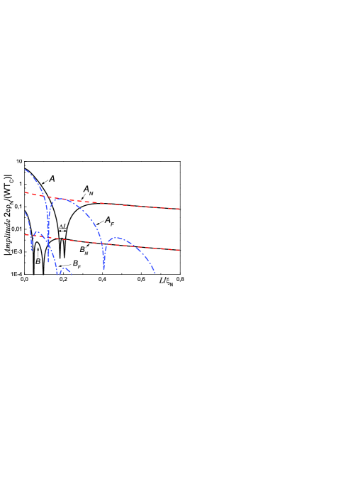
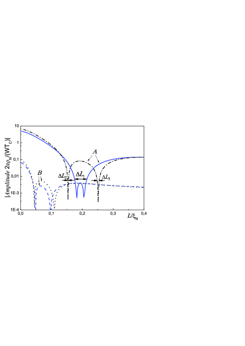
The boundary problem (4)-(9b) has been solved numerically for the same set of junction parameters except The results of calculations for and are shown in Fig.4 and Fig.5. The solid lines in Fig.4 are the modulus of the amplitudes of the first, and the second, harmonic of CPR as a function of distance between S electrodes. The dashed and dash-dotted lines demonstrate the contributions to these amplitudes from the currents flowing in N and F films, respectively. All the amplitudes were normalized on the same factor It is seen that the main difference between analytical solutions presented in Fig.3 and the curves calculated numerically are located in region of small It is also seen that amplitudes of first and second harmonics of the part of the current flowing in the N film slightly decay with increase. The points of transition of the first harmonic amplitude of the part of the current flowing in the F layer is slightly shifted to the right, toward larger . It is also seen that the amplitude of the second harmonic, in the interval of interest in the vicinity of is negligibly small compared to the magnitude of, . As a result, the shape of curves in Fig.3 and Fig.4 is nearly the same, with a little bit larger interval of junction existence for the curve calculated numerically.
Figure 5 demonstrates the same and dependencies as in Fig.4 (solid and dashed lines) together with and curves calculated for (dash-doted and dotted lines). It is clearly seen that for larger we get out of the interval (26) and instead of relatively large zone may have junction in two very narrow intervals and located in the vicinity of transitions of the first harmonic amplitude
V Ramp type overlap (RTO) junctions
Conditions for the existence of junction (25), (26) can be improved by slight modifications of contact geometry, namely, by using a combination of ramp and overlap configurations, as it is shown in Fig.1b. Fig.6 demonstrates numerically calculated spatial distribution of supercurrent in RTO -junction at Josephson phase . The current density is presented by darkness and the arrows give flows directions. The relative smallness of the first harmonics amplitude is provided by opposite currents in N and F films. The main feature of the ramp-overlap geometry is seen to be specific current distribution in the normal layer leading to another CPR shape with dependence on thickness . Further, the current should saturate as a function of , since normal film regions located at distances larger than from SN interface are practically excluded from the process of supercurrent transfer due to exponential decay of proximity-induced superconducting correlations KLO . The specific geometry of the RTO structures makes theoretical analysis of the processes more complex than in ramp contact. Nevertheless, it is possible to find analytical expressions for supercurrent in these structures and to show that the range of parameters providing the existence of state is broader than in the ramp type configuration.
To prove this statement, we consider the RTO structure in most practical case of thin N film
| (32) |
and sufficiently large providing negligibly small suppression of superconductivity in N film due to proximity with F layer. We will assume additionally that electrode spacing is also small
| (33) |
in order to have nonsinusoidal CPR. Under these conditions we can at the first step consider the Josephson effect in overlap SN-N-NS structure. Then, at the second step we will use the obtained solutions to calculate supercurrent flowing across the F part of the RTO structure. The details of calculations are summarized in Appendices C and D. They give that the supercurrent
| (34) |
consists of three components. Expression for the part of current flowing across N film has the form
| (35) |
where and
The term in (34) is the current through one dimensional double barrier SFS structure defined by Eq. (17), while is FN-interface term shown in D. We provide sufficient smallness and neglect it in the following estimations.
As we discussed above, the larger the relative amplitude of the second harmonic (or the lower the temperature of a junction compare to ), the better the conditions for the implementation of a -contact. In the limit we can transform from summation to integration over in (35) and calculate numerically the dependence of amplitudes and
| (36) |
| (37) |
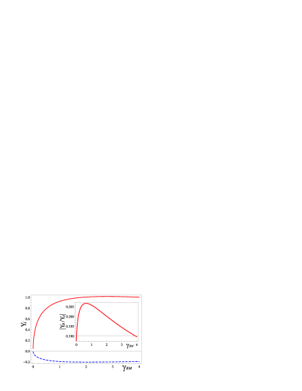
on suppression parameter The calculated dependencies of functions and are presented in Fig.7. It is seen that both and increase with increasing of and saturate at Inset in Fig.7 shows the ratio of the harmonics as a function of . It achieves maximum at thus it determines the optimal values of normalized amplitudes of the first and the second harmonics of the current flowing in the N layer. It is seen from the inset in Fig.7, that the ratio is slowly decreasing function of . Therefore, the estimates given below for are applicable in a wide parameter range .
Taking into account these values, we can write down the condition of -state existence similar to (23)
| (38) |
with slightly modified dimensionless parameter . The wide region of -state still exists if is within the interval
| (39) |
for that satisfies the condition (38). As follows from (38), interval of product gains its maximum length
| (40) |
at . It is seen that these intervals are slightly larger than those given by (25) for the ramp type geometry.
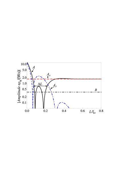
Fig.8 shows the interval of -state existence, in the ideal case of and . The corresponding set of parameters , , , , , , was substituted in (17), (35). The solid line is a modulus of the first harmonic amplitude, , its normal, and ferromagnetic, parts are presented by dashed and dash-dotted lines respectively. Finally, the second harmonic amplitude is shown as dash-dot-dotted line. It’s clear that is relatively small in the wide region and reaches the value of only at local maximum. The increased width of (see Eqs. (29),(49)) is provided by geometric attributes of RTO type structure.
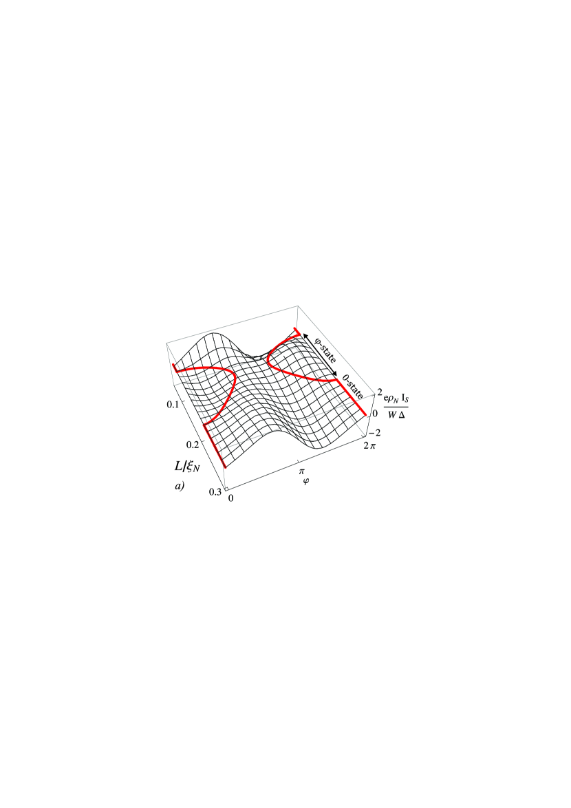
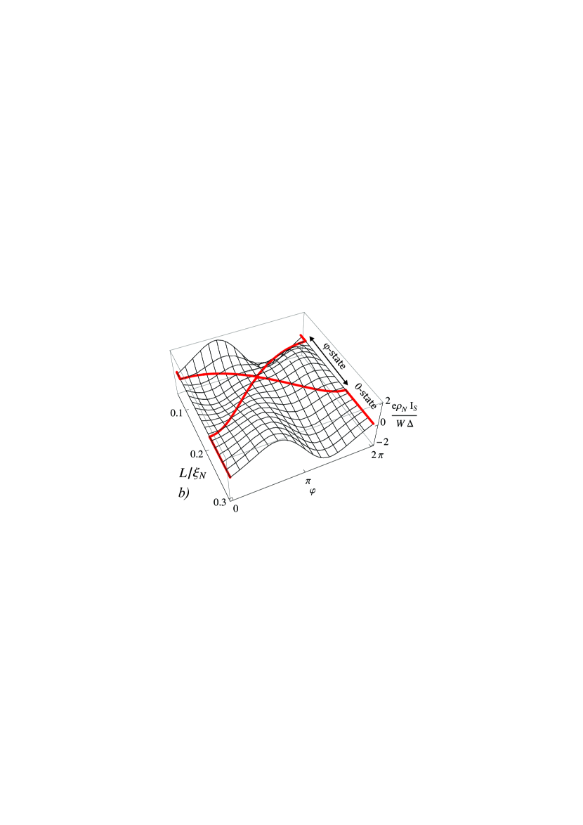
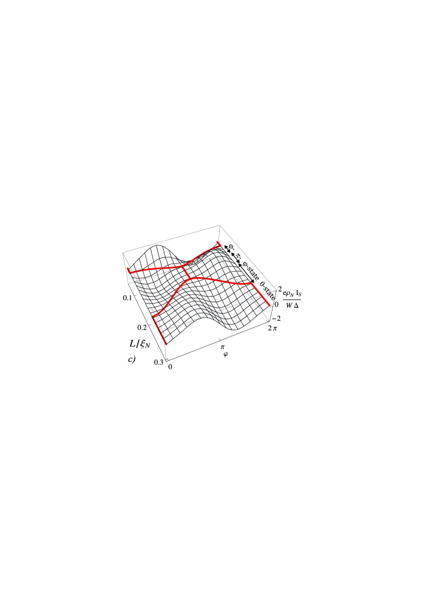
Let us illustrate the range of nontrivial ground phase existence in the structure described in Fig.8. The total supercurrent is shown on Fig.9 as a function of Josephson phase and electrode spacing . It means that each section of this 3D graph is CPR. Solid lines mark the ground state phases at each . In the range of small and large spacing ground phase is located at . However, in the -interval CPR becomes significantly nonsinusoidal and demands ground phase to split and go to from both sides; then state is realized at . Clearly, for the value can not be reached (see Fig.9a), while in the case of the prolonged -state region is formed (see Fig.9c).
VI Discussion
We have shown that stable -state can be realized in S-NF-S structures with longitudinally oriented NF-bilayers (though -state can not be achieved in conventional SNS and SFS structures). We have discussed the conditions for realization of -state in ramp-type S-NF-S and RTO-type SN-FN-NS geometries.
Let us discuss most favorable conditions for for experimental realization of -junction. We suggest to use Copper as a normal film ( and ) and strongly diluted ferromagnet like FePd or CuNi alloy as the F-layer. We chose Nb as a superconducting electrode material since it is commonly used in superconducting circuits applications. We also propose to use sufficiently thick normal layer, above the saturation threshold, when N-layer thickness have almost no effect. After substitution of relevant values into (39) and (40) we arrived at a fairly broad geometrical margins, within which there is a possibility for implementation of -junctions
| (41) | |||||
Finally, the last out-of-plane geometrical scale is set as . This value maximizes current and conserves the scale of structure in a range of . The magnitude of critical supercurrent in the -state is determined by the second harmonic amplitude
| (42) |
The spreads of geometrical scales as well as the magnitude of critical current are large enough to be realized experimentally.
By creating -state in a Josephson junction one can fix certain value of ground phase . Temperature variation slightly shifts the interval of relevant - transition and permits one to tune the desired ground state phase. Furthermore, sensitivity of the ground state to an electron distribution function permits -junctions to be applied as small-scale self-biasing one-photon detectors. Moreover, quantum double-well potential is formed at the point of ground state splitting providing necessary condition for quantum bits and quantum detectors. To summarize, Josephson -junctions can be realized using up-to-date technology and may become important basic element in superconducting electronics.
Acknowledgements.
We gratefully acknowledge V. V. Ryazanov helpful discussions. This work was supported by the Russian Foundation for Basic Research (Grants 12-02-90010-Bel-a, 11-02-12065-ofi-m), Russian Ministry of Education and Science, Dynasty Foundation and Dutch FOM.Appendix A Ramp type junctions. Limit of small
In the limit of small spacing between S electrodes
| (43) |
we can neglect nongradient terms in (4)
| (44) |
| (45) |
and introduce four functions
| (46) |
where, is imaginary unit, and are even function of coordinate while and are odd in Due to the symmetry at
| (47) |
for any coordinate and it is convenient to rewrite boundary conditions (9a), (9b) at in the form
| (48a) | ||||
| (48b) | ||||
| (49a) | ||||
| (49b) | ||||
| At NF interface the boundary conditions transforms to: | ||||
| (50a) | ||||
| (50b) | ||||
| (51a) | ||||
| (51b) | ||||
| From (47) and (48a) - (49b) it follows that for and within the interval | ||||
| (52) |
we can neglect in left hand side of (49a), (49b). Moreover, in this approximation for any point inside the weak link region and the boundary problem (44)-(51b) for functions and can be solved resulting in
| (53) |
and
| (54) |
Therefore under conditions (52) both and are independent on coordinate functions and equations for transform to Laplas equations, which have the solutions
| (55) |
| (56) |
They automatically satisfy the boundary conditions at and as well as at and To find the integration constants and we have to substitute (55) and (56) into (51a), (51b) and get
| (57) |
where
and
Substitution of (55) and (56) into expression for the supercurrent (5) gives that contributions to the supercurrent across the junction proportional to and cancel each other and equals to the sum
| (58) |
| (59) |
of the currents, and, flowing independently across F and N parts of the weak link.
Appendix B Ramp type junctions. Limit of intermediate
For intermediate values of spacing between the S electrodes
| (60) |
and suppression parameters at SN and SF interfaces belonging to the interval (3) the boundary problem (4)-(9b) can be also solved analytically for sufficiently large suppression parameter Under these restrictions in the first approximation we can neglect the suppression of superconductivity in the N film due to proximity with the F layer and use expressions (53) and (56) with as the solution in the N part of the weak link.
To find and we have to solve the linear equations
| (61) |
| (62) |
with the boundary conditions
| (63) |
| (64) |
at and
| (65) |
| (66) |
at ( The boundary problem (61)-(66) must be closed by the conditions (7) and (47) at free interface of the F film and at the line of junction symmetry, respectively.
Spatial distribution of even in coordinate part of can be found in the form of superposition of superconducting correlations induced into F film from superconductors and from the N part of weak link
| (67) |
Solution for the odd part of consists of three terms
| (68) |
where The first two give the part of induced from the N film, while the last has the well known for SFS junction formRevG ,RevB ,RevV .
From (67) and (68) it follows that and Substitution of (67) and (68) into expression for the supercurrent (5) gives that the dependence is consists of three terms
| (69) |
The first is the supercurrent across the N layer. In considered approximation it coincides with the expression given by (58). The second term in (69) is the supercurrent across SFS double barrier structure in the limit of small transparencies of SF interfacesGolubov1 ,DBbuz
| (70) |
and the last consists of two terms, having different dependence
| (71) |
| (72) |
where In real experimental situation
| (73) |
Under the conditions (73) some terms of can be neglected. Still existing expressions of it parts - simplify to
| , | (74) |
| (75) |
| (76) |
.
Appendix C Overlap SN-N-NS junctions.
To calculate critical current of SN-N-NS junctions we consider the most practical case of thin N film
| (77) |
and sufficiently large providing the absence of suppression of superconductivity in N film due to proximity with F layer. We will also assume that electrode spacing is also small
| (78) |
in order to have nonsinusoidal CPR.
Condition (77) permits to perform averaging of Usadel equations in direction in N film, as it was described in detail in Karminskaya , and reduce the problem to the solution of one dimensional equations for . The real part of is the solution of the boundary problem
| (79) |
| (80) |
| (81) |
where
From (80), (81) it follows that at functions are independent on constants resulting in
| (82) |
The arising boundary problem (79), (81), (82) is also satisfied by independent on constants leading to
| (83) |
Introducing now new functions,
| (84) |
where we get
| (85) |
| (86) |
| (87) |
where
| (88) |
| (89) |
Solution of Eq. (86) can be easily found
| (90) |
Solution of Eq. (85) can be simplified due to existence of the first integral
| (91) |
The constant of integration in the right hand side of (91) have been found from the boundary condition (87), which demands then Further integration in (91) for gives
| (92) |
where is integration constant, which should be determined from the matching conditions at For they give
| (93) |
Assuming additionally that is not too small, namely that from (93) it is easy to get
| (94) |
resulting in
| (95) |
From (95) it follows that in weak link region
| (96) |
while under the S electrode,
| (97) |
Appendix D Solution in Ferromagnet Layer of RTO junction.
Spatial distribution of even and odd in coordinate parts of can be found in the form of superposition of superconducting correlations induced into F film from superconductors and from the N part of weak link. It has the same form as in (67) and (68)
| (99) |
| (100) |
with the functions and defined by equations followed from the solution of the boundary problem in the N layer described in Appendix C.
| (101) |
| (102) |
Substitution of (99)-(102) into expression (5) gives that supercurrent across F layer in RTO junction consists of the sum of and , where is the current through one dimensional double barrier SFS structure defined by Eq. (70), while has the form
| (103) |
| (104) |
Application of conditions (73) allows to neglect some terms in and to simplify remaining terms, leading to the following expressions:
| , | (105) |
| = | (106) |
| (107) |
References
- (1) K.K. Likharev, Rev. Mod. Phys. 51, 101 (1979).
- (2) A. A. Golubov, M. Yu. Kupriyanov, E. Il’ichev, Rev. Mod. Phys. 76, 411 (2004).
- (3) A. I. Buzdin, Rev. Mod. Phys. 77, 935 (2005).
- (4) F. S. Bergeret, A. F. Volkov, K. B. Efetov, Rev. Mod. Phys. 77, 1321 (2005).
- (5) V. V. Ryazanov, V. A. Oboznov, A. Yu. Rusanov, A. V. Veretennikov, A. A. Golubov, and J. Aarts, Phys. Rev. Lett. 86, 2427 (2001).
- (6) S. M. Frolov, D. J. Van Harlingen, V. A. Oboznov, V. V. Bolginov, and V. V. Ryazanov, Phys. Rev. B 70, 144505 (2004);
- (7) T. Kontos, M. Aprili, J. Lesueur, F. Genet, B. Stephanidis, and R. Boursier, Phys. Rev. Lett. 89, 137007 (2002).
- (8) H. Sellier, C. Baraduc, F. Lefloch, and R. Calemczuck, Phys. Rev. B 68, 054531 (2003).
- (9) Y. Blum, A. Tsukernik, M. Karpovski, and A. Palevski, Phys. Rev. B 70, 214501 (2004).
- (10) C. Surgers, T. Hoss, C. Schonenberger, C. Strunk, J. Magn. Magn. Mater. 240, 598 (2002).
- (11) C. Bell, R. Loloee, G. Burnell, and M. G. Blamire Phys. Rev. B 71, 180501 (R) (2005).
- (12) S. M. Frolov, D. J. Van Harlingen, V. V. Bolginov, V. A. Oboznov, and V. V. Ryazanov, Phys. Rev. B 74, 020503 (2006).
- (13) V. A. Oboznov, V. V. Bol’ginov, A. K. Feofanov, V. V. Ryazanov, and A. I. Buzdin, Phys. Rev. Lett. 96, 197003 (2006).
- (14) V. Shelukhin, A. Tsukernik, M. Karpovski, Y. Blum, K. B. Efetov, A. F. Volkov, T. Champel, M. Eschrig, T. Lofwander, G. Schon, and A. Palevski, Physical Review B 73, 174506 (2006).
- (15) M. Weides, K. Tillmann, and H. Kohlstedt, Physica C 437-438, 349 (2006).
- (16) M. Weides, M. Kemmler, H. Kohlstedt, A. Buzdin, E. Goldobin, D. Koelle, R. Kleiner, Appl. Phys. Lett. 89, 122511 (2006).
- (17) M. Weides, M. Kemmler, H. Kohlstedt, R. Waser, D. Koelle, R. Kleiner, and E. Goldobin Physical Review Letters 97 247001 (2006).
- (18) J. Pfeiffer, M. Kemmler, D. Koelle, R. Kleiner, E. Goldobin, M. Weides, A. K. Feofanov, J. Lisenfeld, and A. V. Ustinov, Physical Review B 77, 214506 (2008).
- (19) H. Sellier, C. Baraduc, F. Lefloch, and R. Calemczuck, Phys. Rev. Lett. 92, 257005 (2004).
- (20) F. Born, M. Siegel, E. K. Hollmann, H. Braak, A. A. Golubov, D. Yu. Gusakova, and M. Yu. Kupriyanov, Phys. Rev. B. 74, 140501 (2006).
- (21) J. W. A. Robinson, S. Piano, G. Burnell, C. Bell, and M. G. Blamire, Phys. Rev. Lett. 97, 177003 (2006).
- (22) S. Piano, J. W.A. Robinson, G. Burnell, M. G. Blamire The European Physical Journal B 58, 123 (2007).
- (23) J. W. Robinson, S. Piano, G. Burnell, C. Bell, and M. G. Blamire Physical Review B 76, 094522 (2007).
- (24) R. S. Keizer, S. T. B. Goennenwein, T. M. Klapwijk, G. Miao, G. Xiao, A. Gupta, Nature 439, 825 (2006).
- (25) T. S. Khaire, M. A. Khasawneh, W. P. Pratt, Jr., and N. O. Birge, Phys. Rev. Lett. 104, 137002 (2010).
- (26) J. W. A. Robinson, J. D. S. Witt, and M. G. Blamire, Science 329, 59 (2010).
- (27) J.Wang, M. Singh, M. Tian, N. Kumar, B. Liu, C. Shi, J. K. Jain, N. Samarth, T. E. Mallouk and M. H. W. Chan, Nat. Phys. 6, 389 (2010).
- (28) M. S. Anwar, F. Czeschka, M. Hesselberth, M. Porcu, and J. Aarts, Phys. Rev. B 82, 100501(R) (2010).
- (29) M. S. Anwar, M. Veldhorst, A. Brinkman, and J. Aarts, Appl. Phys.Lett. 100, 052602 (2012).
- (30) T. Ortlepp, Ariando, O. Mielke, C. J. M. Verwijs, K. F. K. Foo, H. Rogalla, F. H. Uhlmann, and H. Hilgenkamp, Science 312, 1495 (2006).
- (31) A.K. Feofanov, V.A. Oboznov, V.V. Bol’ginov, et. al., Nature Physics 6, 593 (2010).
- (32) A. V. Ustinov and V. K. Kaplunenko, J. Appl. Phys. 94, 5405 (2003).
- (33) R.G. Mints, Phys. Rev. B 57, R3221 (1998).
- (34) A. Buzdin and A. E. Koshelev, Phys. Rev. B 67, 220504(R) (2003).
- (35) N. G. Pugach, E. Goldobin, R. Kleiner, and D. Koelle, Phys. Rev. B 81, 104513 (2010).
- (36) M.Yu. Kupriyanov, A.A. Golubov, M. Siegel, Proceedings of the SPIE, 6260, 62600S-1 (2006).
- (37) E. Goldobin, D. Koelle, R. Kleiner, and R.G. Mints, Phys. Rev. Lett, 107, 227001 (2011); H. Sickinger, A. Lipman, M Weides, R.G. Mints, H. Kohlstedt, D. Koelle, R. Kleiner, and E. Goldobin, arXiv 1207.3013.
- (38) E. Goldobin, D. Koelle, R. Kleiner, and A. Buzdin, Phys. Rev. B, 76, 224523 (2007).
- (39) N. V. Klenov, N. G.Pugach, A. V.Sharafiev, S. V.Bakurskiy, V. K.Kornev, Physics of Solid State, 52, 2246 (2010).
- (40) A. S. Vasenko, A. A. Golubov, M. Yu. Kupriyanov, and M. Weides, Phys.Rev.B, 77 134507 (2008).
- (41) A. S. Vasenko, S. Kawabata, A. A. Golubov, M. Yu. Kupriyanov, C. Lacroix, F. W. J. Hekking, Phys. Rev. B 84 024524 (2011).
- (42) F. Konschelle, J. Cayssol, A.I. Buzdin, Phys. Rev. B 78, 134505 (2008).
- (43) M. Houzet, V. Vinokur, and F. Pistolesi, PRB 72, 220506 (2005)
- (44) T. Yu. Karminskaya and M. Yu. Kupriyanov, Pis’ma Zh. Eksp. Teor. Fiz. 85, 343 (2007) [JETP Lett. 85, 286 (2007)].
- (45) T. Yu. Karminskaya and M. Yu. Kupriyanov, Pis’ma Zh. Eksp. Teor. Fiz. 85, 343 (2007) [JETP Lett. 86, 61 (2007)].
- (46) T. Yu. Karminskaya, M. Yu. Kupriyanov, and A. A. Golubov, Pis’ma Zh.Eksp. Teor. Fiz. 87, 657 (2008) [JETP Lett., 87, 570 (2008)].
- (47) Karminskaya T. Yu., Golubov A. A., Kupriyanov M. Yu., Sidorenko A. S., Phys.Rev.B 79, 214509 (2009).
- (48) T. Yu. Karminskaya, A. A. Golubov, M. Yu. Kupriyanov, and A. S. Sidorenko Phys. Rev. B 81, 214518 (2010).
- (49) S. V. Bakurskiy, N. V. Klenov, T. Yu. Karminskaya, M. Yu. Kupriyanov and V. K. Kornev, Solid State Phenomena, 190, 401 (2012).
- (50) F. S. Bergeret, A. F. Volkov, and K. B. Efetov, Phys. Rev. Lett. 86, 3140 (2001).
- (51) Ya. V. Fominov, N. M. Chtchelkatchev, and A. A. Golubov, Phys. Rev. B 66, 014507 (2002).
- (52) A. Furusaki and M. Tsukada, Solid State Commun. 78, 299 (1991).
- (53) A. Furusaki and M. Tsukada, Phys. Rev. B 43, 10 164 (1991).
- (54) Z. G.Ivanov, M. Yu. Kupriyanov, K. K. Likharev, S. V. Meriakri, and O. V. Snigirev, Fiz. Nizk. Temp. 7, 560 (1981). [Sov. J. Low Temp. Phys. 7, 274 (1981)]
- (55) A. A.Zubkov, and M. Yu. Kupriyanov, Fiz. Nizk. Temp. 9, 548 (1983) [Sov. J. Low Temp. Phys. 9, 279 (1983)].
- (56) M. Yu. Kupriyanov, Pis’ma Zh. Eksp. Teor. Fiz. 56, 414 (1992). [JETP Lett. 56, 399 (1992)].
- (57) Demler, E. A., Arnold G. B., and Beasley M. R., Phys. Rev. B 55, 15174 (1997).
- (58) K. D. Usadel, Phys. Rev. Lett. 25, 507 (1970).
- (59) M. Yu. Kuprianov and V. F. Lukichev, Sov. Phys. JETP 67, 1163 (1988) [Zh. Eksp. Teor. Fiz. 94, 139 (1988)].
- (60) N. M. Chtchelkatchev and I. S. Burmistrov, Phys. Rev. B 68, 140501(R) (2003).
- (61) I. S. Burmistrov and N. M. Chtchelkatchev, Phys. Rev. B 72, 144520 (2005).
- (62) T. Champel and M. Eschrig, PRB 72, 054523 (2005).
- (63) M. Houzet and A. I. Buzdin, Phys. Rev. B 74, 214507 (2006).
- (64) M. A. Maleki and M. Zareyan Physical Review B 74, 144512 (2006).
- (65) Y. V. Fominov, A. F. Volkov, and K. B. Efetov, Phys. Rev. B 75, 104509 (2007).
- (66) A. F. Volkov and A. Anishchanka, Phys. Rev. B 71, 024501 (2005).
- (67) A.F. Volkov, K.B. Efetov Phys Rev B 78, 024519 (2008).
- (68) B. Crouzy, S. Tollis, D. A. Ivanov, Phys. Rev. B 76, 134502 (2007).
- (69) A. A. Golubov, M. Yu. Kupriyanov, and Ya. V. Fominov, JETP Lett. 75, 709 (2002) [Pisma v ZhETF 75, 588 (2002)].
- (70) A. Buzdin, JETP Lett. 78, 1073 (2003) [Pisma v ZhETF 78, 1073 (2003)].
- (71) M. Yu.Kupriyanov, V. F. Lukichev, A. A. Orlikovskii, Mikroelektronika 15, 328 (1986) [Soviet Microelectronics 15, 185 (1986)].