How to modify the van der Waals and Casimir forces without change of dielectric permittivity
Abstract
We propose a new experiment on measuring the Casimir force and its gradient between an Au-coated sphere and two different plates made of doped semiconductors. The concentrations of charge carriers in the plates are chosen slightly below and above the critical density at which the Mott-Anderson insulator-metal transition occurs. We calculate changes in the Casimir force and the Casimir pressure due to the insulator-metal transition using the standard Lifshitz theory and the phenomenological approach neglecting the contribution of free charge carriers in the dielectric permittivity of insulator materials (this approach was recently supported by the measurement data of several experiments). It is demonstrated that for the special selection of semiconductor materials (S- or Se-doped Si, B-doped diamond) calculation results using both theoretical approaches differ significantly and the predicted effects are easily detectable using the existing laboratory setups. In the case that the prediction of the phenomenological approach is confirmed, this would open opportunities to modify the van der Waals and Casimir forces with almost no change of room temperature dielectric permittivity.
pacs:
71.30.+h, 61.72.sd, 74.25.Gz, 12.20.Fv1 Introduction
The van der Waals and Casimir forces act between closely spaced material surfaces [1, 2]. These forces are the manifestations of the so-called dispersion forces caused by the zero-point and thermal fluctuations of the electromagnetic field. The distance range of dispersion forces extends from several angströms to a few nanometers (the van der Waals regime where the relativistic retardation is not important) and from a few nanometers to a few micrometers (the Casimir regime where the retardation effects contribute more and more as the separation distance increases). The diverse applications of dispersion forces vary from the physics of surface and nanostructures [3, 4, 5, 6, 7, 8, 9, 10] to obtaining constraints on the predictions of unification theories of fundamental interactions beyond the Standard Model [11, 12, 13].
The van der Waals and Casimir forces are entirely quantum phenomena. Theory of these phenomena goes back to the classical papers by London [14] and Casimir [15], respectively. Much work in the theory of dispersion forces was done by Langreth and his coworkers by developing a density functional that includes van der Waals interaction [16]. For plane-parallel layered structures described by the frequency-dependent dielectric permittivities the exact theory of the van der Waals and Casimir forces was developed by Lifshitz [17, 18]. In the last few years the main equations of the Lifshitz theory were generalized for bodies of arbitrary shape [19, 20, 21]. This allowed the development of explicit expressions for the free energy and force in the experimentally relevant configurations, such as a material sphere above a material plate [22, 23]. According to the Lifshitz theory and its generalizations, in order to modify the van der Waals and Casimir forces, it is necessary to change the reflection properties of boundary surfaces over a wide frequency range.
Starting in 1997, a lot of experiments on measuring dispersion forces between bodies made of different materials have been performed using modern laboratory techniques made possible by micro- and nanotechnology (reviews [24, 25, 26] contain detailed description of all experiments with the exception of the most recent [27, 28, 29, 30, 31]). All these experiments measured dispersion forces in the retarded regime, i.e., thermal Casimir forces. Experimental investigation of dispersion forces at sufficiently high precision leads us to recognize that this phenomenon is much more complicated than it was generally believed in the past based on the Lifshitz theory. The facts suggesting so radical a conclusion are the following.
In a series of dynamic experiments [32, 33, 34, 35] on measuring the thermal Casimir pressure between two Au plates by means of a micromachined oscillator it was found that the experimental data exclude the predictions of the Lifshitz theory at K obtained using the optical data of Au extrapolated to low frequencies by means of the Drude model (this calculation approach to the thermal Casimir force was used in 2000 [36]). The same data turned out to be consistent with the predictions of the Lifshitz theory obtained when free charge carriers are described using the plasma model. Keeping in mind that the dielectric permittivity of the Drude model at low frequencies is inversely proportional to the frequency, as it should be in accordance with the Maxwell equations, whereas the plasma model neglects relaxation and is approximately applicable only at sufficiently high frequencies, this result should be considered as a big surprise. Recently similar measurements were independently performed by another technique [i.e., with the help of an atomic force microscope (AFM) operated in the dynamic regime [37, 38]] with the same result. For completeness we note that there are also two experiments [39, 40] on the observation of the Casimir force between Au-coated spherical lenses of more than 10 cm radii of curvature and an Au-coated plate performed by means of a torsion pendulum. These are not independent measurements of the Casimir force because they are based on the fit between the experimental data and theoretical predictions with some fitting parameters. One of these experiments [39] is in support of the plasma model and the other one [40] is in favor of the Drude model (critical analysis of experiments with large spherical lenses is provided in the literature [41, 42, 43]). Recent experiment using a nanomembrane resonator [44] also claims a support of the Drude model, but the comparison of experiment with theory was shown to be in error [45].
Additional evidence comes from measurements [46, 47] of the difference in the Casimir force between an Au sphere and Si plate at K in the presence and in the absence of a laser pulse on a plate. The laser pulse led to a 5 orders of magnitude increase of the free charge carrier density in the Si sample and respective change of the dielectric permittivity. The experimental data were found to be consistent with the Lifshitz theory if the contribution of free charge carriers to the dielectric permittivity in the absence of a laser pulse (i.e., in the dark phase when Si is a dielectric-type semiconductor) is omitted. In so doing the Casimir force is determined by the contribution of bound electrons alone. If the free charge carriers in the dark phase are included, the theory is found to be inconsistent with the data. The reason exactly why existing free charge carriers do not contribute to the force magnitude remains unclear. Note that according to the Lifshitz theory bound charge carriers give a more important contribution to the van der Waals and Casimir forces at shorter separations, whereas the contribution of free charge carriers increases with increasing separation.
A similar situation was observed in measurements [48] of the thermal Casimir-Polder force between 87Rb atoms belonging to the Bose-Einstein condensate and SiO2 plate. The measurement data were found [48] to be consistent with the predictions of the Lifshitz theory if dc conductivity of the plate is omitted. If, however, the dc conductivity of SiO2 is included in computations, the obtained theoretical results turn out to be in disagreement with the data [49].
Another surprise was from the measurements [29, 30, 50] of the thermal Casimir force at K between an Au-coated sphere and an indium tin oxide (ITO) film deposited on a quartz substrate. At room temperature ITO is a good conductor at low frequencies, but is transparent to visible and near infrared light. Based on these properties, ITO was considered [51] as a very prospective material in experiments on measuring the Casimir force which require good dc conductivity to correct for residual electrostatic forces. Measurements of the gradient of the Casimir force between an Au sphere and an ITO plate [52, 53] demonstrated that it is 40%–50% smaller than between an Au sphere and an Au plate. It was shown [29, 30, 50] that after the UV treatment of an ITO plate the magnitude of the Casimir force further decreases from 21% to 35% depending on separation. Surprisingly, this decrease is not accompanied by respective changes in the dielectric permittivity of ITO which could explain the change in the force based on the Lifshitz theory. To bring the data into agreement with theory it was necessary to omit the contribution of free charge carriers in the UV-treated ITO film. It was hypothesized [29, 30, 50] that the UV treatment caused a Mott-Anderson transition in ITO from a metal to an insulating state without significant changes in the optical and electrical properties at room temperature. Then the observed agreement of the data with the Lifshitz theory when the contribution of free charge carriers for the UV-treated sample is omitted becomes compartible with the results of other experiments [46, 47, 48, 49] discussed above. It should be noted also that the Lifshitz theory taking into account the static conductivity for dielectric materials or the relaxation properties of conduction electrons for metals with perfect crystal lattices was proved [2, 24, 51, 54] to violate the third law of thermodynamics (the Nernst heat theorem). In fact the problems arising in the Lifshitz theory for both metals and dielectrics have generic roots in the foundations of quantum statistical physics [55].
In this paper we propose a new experiment which could provide direct validation or disproof of the statement that the transition of a material from insulating to metal state results in a significant change of the Casimir force even if the dielectric permittivity remains nearly unchanged. In the optical modulation experiment [46, 47], where a Si plate was radiated with laser pulses, the free charge carrier density in the absence of a pulse was much smaller than the critical concentration at which Si becomes metallic. As a result, the contributions of free charge carriers in the absence and in the presence of laser light were quite different.
Here we propose that the Casimir force or its gradient should be compared between an Au sphere and the two plates made of doped semiconductor one of which has the doping concentration slightly below and the other one slightly above the critical value [56]. This ensures that the dielectric properties of both plates at room temperature are almost identical [56] so that minor differences between them cannot lead to large change in the magnitude of the Casimir force between the sphere and each of the plates when this change is calculated using the standard Lifshitz theory. As a direct check of the fact that the dielectric permittivities of both plates are almost identical, their optical properties over a wide frequency region should be investigated by means of ellipsometry as was done for ITO samples [29, 30, 50]. In order to increase the possible change in the Casimir force when passing from the first plate to the second, we choose doped semiconductor with the critical concentration of charge carriers of order (such as boron-doped diamond or sulphur-doped Si). As demonstrated below, this would ensure the increase in the magnitudes of the Casimir force or its gradient up to 30% when replacing the insulator-type plate with the metal-type plate if the effect of Mott-Anderson transition on dispersion forces does occur, as is anticipated based on previous experiments [29, 30, 50]. Such a large relative change predicted allows reliable measurement of the effect under discussion with the already built and operated laboratory setups.
The paper is organized as follows. In Sec. 2 we present the main mathematical expressions for the calculation of dispersion forces and make the choice of optimal materials. Section 3 is devoted to the calculation of the force and force gradient for an Au sphere interacting with a plate made of S-doped silicon when the plate material undergoes a transition from insulating to metal state. In Sec. 4 the same calculation is performed for a plate made of B-doped diamond. In Sec. 5 the reader will find our conclusions and discussion.
2 Expressions for the calculation of dispersion forces and choice of materials
We propose to measure in succession the Casimir interaction between an Au-coated sphere and two plates coated with some doped semiconductor films whose free charge carrier densities are slightly below and slightly above the critical value specific for this semiconductor. Measurements will be performed by means of an AFM operated either in the static mode [29, 30] or in the dynamic mode in the frequency shift technique [37, 38]. In the static regime, the directly measured quantity is the Casimir force between the sphere and the plate whereas in the dynamic regime it is the gradient of the Casimir force , where is the separation distance between the sphere and the plate. The gradient of the Casimir force between a sphere and a plate can be simply reformulated into the Casimir pressure between the two parallel plates (one made of Au and the other one consists in a semiconductor film deposited on a substrate) using the proximity force approximation [2, 24]
| (1) |
Note that the error from the use of the PFA in the sphere-plate geometry for a sphere and a plate made of real materials was recently shown [23] to be less than , i.e., about 0.1% for the experimental parameters. Because of this, one can safely use this approximation below in computations based on the Lifshitz theory.
Using the Lifshitz formula for the free energy in the configuration of two parallel plates and the PFA, the Casimir force between an Au sphere of radius and a semiconductor film deposited on a substrate at temperature can be written as
| (2) |
Here, is the Boltzmann constant, with are the Matsubara frequencies, the prime near the summation sign means that the term with is divided by 2, is the projection of the wave vector onto the plate, and . The reflection coefficients of an Au coating modeled as a semispace, , for the transverse magnetic (TM) and transverse electric (TE) polarizations of the electromagnetic field are presented in the form
| (3) |
where is the dielectric permittivity of Au along the imaginary frequency axis and .
The reflection coefficients of a doped semiconductor film of thickness deposited on a thick substrate plate modeled as a semispace are given by [2, 57]
| (4) |
and by a similar expression for with the index TM replaced for TE in (4). Here, are the reflection coefficients on a semiconductor film () and on a substrate ()
| (5) |
where and are the dielectric permittivities of the semiconductor film and the substrate material, respectively, and is the permittivity of the vacuum gap. We also use the notation with [note that ].
The Casimir pressure at a temperature , which is calculated using (1) from the gradient of the Casimir force measured in the dynamic regime, is given by
| (6) |
where the reflection coefficients for our configuration are already defined in (3)–(5).
Equations (2) and (6) can be used to calculate the Casimir force between an Au sphere and a semiconductor film deposited on a substrate and the Casimir pressure between an Au plate and the same film on a substrate. This can be done in two different ways: by the immediate substitution of the dielectric permittivity along the imaginary frequency axis, as obtained using the Kramers-Kronig relation from the measured optical data (this way is suggested by the standard Lifshitz theory) and by omitting the contribution of free charge carriers when the semiconductor film is in an insulating state (this way is suggested by the experimental results discussed in Sec. 1). Below we choose semiconductor materials leading to the largest difference between the computational results obtained in both ways.
Note that an experiment similar in spirit to the one proposed here was performed [25, 58] with two P-doped Si plates which possess, however, radically different densities of free charge carriers. For the first plate interacting with an Au sphere the concentration of free charge carriers was , and for the second . Thus, these concentrations were approximately two orders of magnitude lower, respectively, higher than the critical concentration for a P-doped Si equal to [59] . Keeping in mind the rather high static dielectric permittivity, , the P-doped Si does not seem a good candidate for the experiment proposed here. In a similar way, B-doped Si ( [60]) or Sb-doped Ge ( [59]) are not preferable for using in the proposed experiment.
Another situation holds for a Si doped by S or Se. For a S-doped Si the critical concentration of free charge carriers falls in between , when this semiconductor is an insulator, and when it is of metallic-type [61]. For a Se-doped Si the critical concentration is confined between [62] (semiconductor of dielectric-type) and (semiconductor of metallic-type).
One more prospective material for the purposes of the proposed experiment is boron-doped diamond. For this semiconductor the dielectric-metal transition occurs at [63] . Depending on the preparation technology, the static dielectric permittivity of B-doped C is confined between 5.5 and 10. This semiconductor, demonstrating many interesting properties including superconductivity, is a good candidate for use in the proposed experiment.
The semiconductor materials discussed above will be used in computations of Secs. 3 and 4 in order to determine the feasibility of the experiment under discussion.
3 Change of dispersion forces due to dielectric to metal transition in doped silicon
To perform computations of the Casimir force between a sphere and a plate and the Casimir pressure between two flat plates we need the dielectric permittivities of all materials under discussion along the imaginary frequency axis. They are going to be obtained from the reflectivity data measured by means of ellipsometry for the samples used in experiments. For preliminary theoretical investigation the tabulated optical data for Si can be used [64]. A less than 1% error in the magnitude of the Casimir force, as compared with the tables, is given by the following analytical approximation suggested for high-resistivity Si [65]:
| (7) |
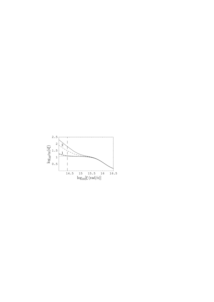
where rad/s and . In figure 1 the behavior of as a function of frequency is shown by the grey line.
The dielectric permittivity of doped Si along the imaginary frequency axis is given by [64]
| (8) |
where is the relaxation parameter and the plasma frequency is expressed in terms of the effective mass of an electron and the concentration of free charge carriers by the equation
| (9) |
Here, is the permittivity of vacuum and is the electron charge.
Now we consider two S-doped Si plates with and . These are -type semiconductors with where is the mass of an electron. From (9) one obtains rad/s and rad/s (rad/s). The respective dielectric permittivities (8) along the imaginary frequency axis are shown in figure 1 by the dashed and solid lines marked 2. The first Matsubara frequency at K is indicated by the vertical long-dashed line.
For comparison purposes we also consider two P-doped Si plates used in a previous experiment [58], but with doping concentrations and , i.e., much closer to the critical value. These are also -type semiconductors characterized by the same effective mass of an electron. The respective values of the plasma frequency calculated using (9) are rad/s and rad/s. The respective dielectric permittivities are shown in figure 1 by the dashed and solid lines marked 1.
In all cases the material of the sphere (Au) is described by the optical data for the complex index of refraction [66] extrapolated to lower frequencies by means of the Drude model with eV, eV. It was recently shown [67] that this extrapolation is in excellent agreement with the optical data measured over a wide frequency region.
3.1 Force between an Au sphere and Si plates
Now we are in a position to calculate the Casimir forces between a sphere and each of the two different Si plates one of which is in metallic and the other in an insulating state. Keeping in mind that technologically there is no problem to prepare Si plates of sufficient thickness, the quantity in (4) can be put equal to infinity so that the reflection coefficients (5) on a Si plate take the same form as the coefficients (3) on Au (the role of finite thickness of a semiconductor film is considered in Sec. 4).

The Casimir forces acting between an Au sphere of m (such a sphere was used in experiments with ITO films [29, 30, 50]) and each of the two S-doped Si plates was calculated by (2). The force values in the case of metallic-type Si decsribed by the dielectric permittivity (the solid line marked 2 in figure 1) are shown by the solid line in figure 2 as a function of separation. The values of the Casimir force for a plate made of insulating-type Si decribed by the permittivity with free charge carriers omitted (the grey line in figure 1) are shown by the dashed line. This line is obtained similar in spirit to the theoretical interpretation of experiments [29, 30, 46, 47, 48, 49, 50] discussed in Sec. 1. As can be seen in figure 2, there is significant relative deviation between the solid and dashed lines that can be observed experimentally with present experimental precision. Thus, the relative difference of sphere-plate Casimir forces with metallic and dielectric plates, , is equal to 7.2%, 10.8%, 15.0%, 18.7%, and 21.8% at separations equal to 60, 100, 150, 200, and 250 nm, respectively. At separations of 450 and 500 nm this relative difference reaches 30.2% and 31.5%, respectively.
This should be compared with the relative force differences for a sphere-plate interaction when the two P-doped Si plates with the doping concentrations and indicated in this section are used (see the solid line marked 1 and the grey line in figure 1). At separation of 60, 100, 150, 200, and 250 nm the relative force differences are equal to 1.1%, 1.6%, 2.2%, 2.8%, and 3.4%, respectively, when the same calculation method is used (i.e., the contribution of free charge carriers is omitted in the dielectric state). At separations of 450 and 500 nm the relative force difference in the case of P-doped Si reaches only 5.7% and 6.2%, respectively. Thus, the replacement of P-doped Si with S-doped Si suggests considerable opportunities in the experimental observation of the effect of insulator-metal transition on the Casimir force in doped semiconductors.
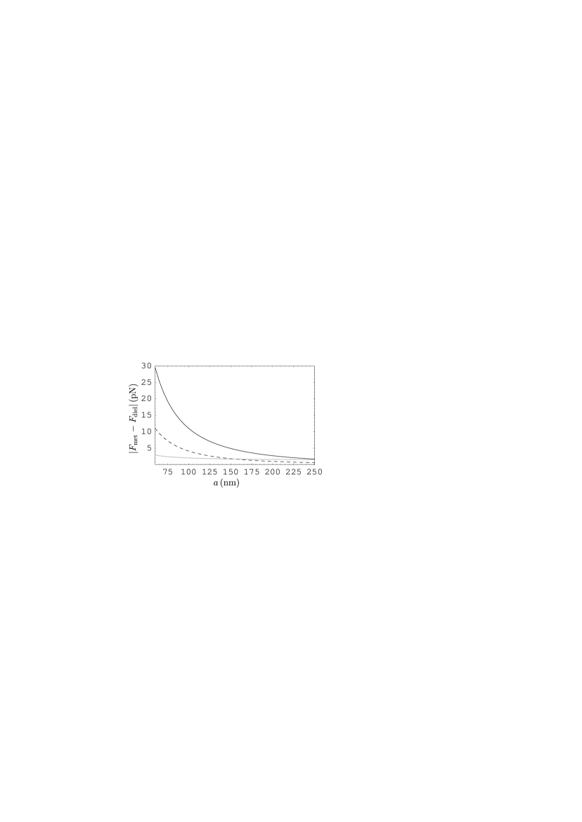
To finally determine the feasibility of the proposed experiment with the plates made of S-doped Si, we compare the absolute changes of the Casimir force due to an insulator-metal transition, , with the total error in the force difference . Here is the total experimental error in the measured Casimir forces determined at a 67% confidence level [29, 30, 50]. In figure 3 we plot the quantity calculated with omitted contribution of free charge carriers in the dielectric state as a function of separation (solid line). In the same figure the total error in the force difference is indicated by the grey line. As can be seen in figure 3, at separations , 100, 150, 200, and 250 nm we obtain , 11.0, 4.9, 2.7, and 1.65 pN, respectively, whereas the respective total errors in the force difference in the recently performed experiment with two ITP plates [29, 30] (the grey line) are equal to , 2.0, 1.8, 1.75, and 1.6 pN. This means that at separations below 250 nm the predicted changes in the Casimir force due to insulator-metal transition in S-doped Si can be reliably detected by using existing experimental setup.
Note that if the exact value of the critical concentration is known we could choose the concentrations and in the insulating and metallic plates, respectively, in such a way that the dielectric permittivities and were almost coincident. In this case nonzero change in the magnitude of the Casimir force due to insulator-metal transition occurs only in the case that the charge carriers in the insulating state are omitted. In our case, however, the proposal is based on the findings of [61] that the sample with charge carriers concentration is in an insulating state, whereas the sample with is in the metallic state. As a result, the respective dielectric permittivities are noticeably different (see the dashed and solid lines marked 2 in figure 1).
Because of this, it is of much interest to compare the above results obtained with the contribution of free charge carriers of the dielectric plate omitted with the results computed by the immediate application of the Lifshitz theory with no additional prescriptions (the dashed line in figure 3). In this case for S-doped Si at separations 60, 100, and 150 nm one obtains , 4.1, and 1.8 pN, respectively, where metallic Si is described by the permittivity and dielectric Si by defined in (8) (see the solid and dashed lines marked 2 in figure 1). It can be seen that the immediate application of the standard Lifshitz theory leads to much smaller force differences although still detectable at separations below 150 nm. These differences are caused by the change of dielectric permittivity, whereas the major contribution to the differences calculated above was caused by the fact that really existing free charge carriers in the dielectric state were omitted.
For the plates made of P-doped Si the insulator-metal phase transition does not lead to a detectable effect. Thus, at separations and 100 nm one obtains and 1.61 pN, respectively, if the contribution of free charge carriers in the dielectric plate is omitted (i.e., the dielectric permittivities shown by the solid line marked 1 and the grey line in figure 1 are used in computations). It is hardly probable that this effect can be detected and if yes at the shortest separations only because pN. As to the immediate application of the standard Lifshitz theory (i.e., using the dielectric permittivities shown by the solid and dashed lines marked 1 in figure 1), at and 100 nm it follows and 0.03 pN, respectively, which is not detectable in the foreseeable future. Thus, the use of Si doped with S offers excellent possibilities to directly check the predictions of the Lifshitz theory for semiconductors which undergo the insulator-metal transition. Dynamic measurements considered in the next section suggest some additional opportunities in this respect.
3.2 Pressure between an Au plate and Si plates
Now we consider the possibilities to observe the effect of insulator-metal transition in a doped semiconductor on the Casimir pressure. As explained in Sec. 2, the Casimir pressure between two parallel plates is obtained from the immediately measured gradient of the Casimir force between a sphere and a plate in the dynamic regime. For this purpose we first compute the Casimir pressure (6) between an Au plate and Si plate using the dielectric permittivity of metallic Si doped with S shown by the solid line marked 2 in figure 1. The magnitude of the obtained pressure is shown by the solid line in figure 4.

For insulating Si with the contribution of charge carriers omitted, the dielectric permittivity along the imaginary frequency axis (7) is shown by the grey line in figure 1. The computational results for the magnitude of the Casimir pressure as a function of separation are shown by the dashed line in figure 4. Here, larger separation distances, than in figure 2 are chosen (as are usually used in dynamic experiments where the separation distance between the sphere and the plate is varied harmonically with time). As can be seen in figure 4, there are significant relative changes in the Casimir pressure due to the insulator-metal transition. Thus, at separations 200, 250, 300, and 350 nm the quantity takes the values 13.9%, 16.8%, 19.5%, and 21.8%, respectively. At nm the relative change in the pressure reaches 27.6%. This is somewhat smaller than for the Casimir force. However, dynamic experiments are more precise than static ones. Because of this, the effect of the phase transition can be observed at larger separations.
To see this, we calculate the absolute change in the Casimir pressure, , under the same conditions as discussed above, i.e., omitting the contribution of free charge carriers in dielectric Si. The values of as a function of separation are shown in figure 5 by the solid line. As a result, at separations , 250, 300, 350, 400, and 450 nm the absolute change in the Casimir pressures takes the values 45.1, 23.1, 13.2, 8.2, 5.3, and 3.6 mPa, respectively. In the recently performed experiment on measuring the Casimir pressure by means of a dynamic AFM operated in the frequency modulation technique [37, 38] the total experimental error in the measured pressure does not depend on separation and is equal to mPa at a 67% confidence level. Thus, the total error in the pressure difference is mPa . It is shown by the grey line in figure 5. By comparing this error with the absolute changes in the Casimir pressure listed above (the solid line in figure 5), we arrive at the conclusion that with the existing setup the effect of the insulator-metal transition on the Casimir pressure can be observed over a separation region from 200 nm to approximately 440 nm.

It is interesting to compare this prediction with the change in the Casimir pressure following from the immediate application of the Lifshitz theory with no omissions. In this case the dielectric permittivities shown by the solid and dashed lines marked 2 in figure 1 are substituted in expression (6) for the Casimir pressure. The obtained pressure differences are plotted in figure 5 by the dashed line. As a result, at separations , 250, 300, and 350 nm the following changes in the magnitude of the Casimir pressure due to dielectric-metal transition are obtained: , 8.5, 4.7, and 2.9 mPa. It can be seen that these changes resulting from real differences in dielectric permittivities of the plates made of S-doped Si are several times less than the changes computed above with the contribution of free charge carriers in dielectric Si omitted. However, from the comparison with the total error in the pressure difference mPa (the grey line in figure 5), one can conclude that even this smaller effect can be observed by means of dynamic measurements at separations from 200 to approximately 315 nm. This makes the proposed experiment vitally important for choosing between competing theoretical approaches.
Computations in this section are done for Si doped with S. Almost the same numerical results are obtained for Si plates doped with Se. As mentioned in Sec. 2, this semiconductor also has high critical doping concentration of order . Because of this, it is also prospective for use in experiments on the impact of Mott-Anderson phase transition on the Casimir effect.
It is worth mentioning also that if metal of the sphere (Au) is described by the generalized plasma-like model [2, 24], which leads to theoretical predictions consistent with the experimental data obtained for two metallic bodies [32, 33, 34, 35, 37, 38], this does not change anything in our conclusions or numerical results.
4 Change of dispersion forces due to the insulator-metal transition in B-doped diamond
As discussed in Sec. 2, another prospective semiconductor material to investigate the influence of insulator-metal transition on the Casimir force, is B-doped diamond. Boron-doped diamond films are usually deposited on silica (SiO2) substrates. For our purposes it is sufficient to use simple analytic approximations for the dielectric permittivity of both materials along the imaginary frequency axis (the experimental samples should be investigated by means of ellipsometry). Thus, for diamond with no doping we get [68]
| (10) |
where , , rad/s, and rad/s. The respective static dielectric permittivity is equal to . In figure 6 the behavior of is shown by the grey line.

The dielectric permittivity of the B-doped diamond is represented similar to (8)
| (11) |
where is defined in (10). We consider two B-doped diamond films with and (see Sec. 2). The respective values of the plasma frequency calculated using (9) rewritten for C instead of Si are rad/s and rad/s. Here, the effective mass has been used [63]. The relaxation parameter in (11) is equal to rad/s [69]. The dielectric permittivities of metallic and dielectric B-doped diamond films are shown in figure 6 by the solid and dashed lines, respectively. The first Matsubara frequency at 300 K is indicated by the vertical long-dashed line.
The parametrization of the dielectric permittivity of SiO2 is given by [68]
| (12) |
where , rad/s, , , , rad/s, rad/s, and rad/s. For the static dielectric permittivity of SiO2 one obtains . In computations below we made sure that the thickness of a B-doped diamond film only slightly influences the values of the Casimir force. The material of the sphere (Au) is described in the same way as in Sec. 3 (i.e., by the tabulated optical data extrapolated to lower frequencies using the Drude model).
4.1 Force between an Au sphere and B-doped diamond films
Now we calculate the Casimir force acting between an Au sphere of m radius and each of the two B-doped diamond films deposited on a SiO2 substrate using (2). In the case of a metallic diamond film the Casimir force as a function of separation is shown by the solid line in figure 7. It was computed with the dielectric permittivity (the solid line in figure 6). For the dielectric diamond film the computational results are shown in figure 7 by the dashed line. These results were obtained with the permittivity (the grey line in figure 6) which does not take into account the free charge carriers. There are significant relative deviations between the two lines in figure 7. Thus, at separations , 100, 150, 200, 300, and 400 nm the quantity is equal to 8.4%, 12.1%, 16.3%, 20.0%, 26.2%, and 31.1%, respectively. At nm this quantity reaches 35.0%.

The above computations were performed for an infinitely thick film (). To determine the role of finite thickness of the diamond film, we calculated the same relative differences in the Casimir force for a film of nm thickness deposited on a silica substrate. Diamond films of about 100 nm thickness are in fact of the minimum thickness used in technological applications. At separations and 100 nm the relative difference in the Casimir force is the same as for an infinitely thick film. Minor changes between these two cases arise only with the increase of separation distance. Thus, for a film of nm thickness at separations , 200, 300, and 400 nm the quantity is equal to 16.4%, 20.2%, 26.8%, and 32.3%, respectively. At nm for a film of nm thickness the relative difference is equal to 36.8%. Comparing with the above results obtained for an infinitely thick semispace made of B-doped diamond, one can conclude that the B-doped diamond film of 100 nm thickness leads to almost the same effect as a semispace.
To determine the feasibility of the proposed experiment with B-doped diamond films, we present the absolute changes in the Casimir force due to insulator-metal transition. This quantity as a function of separation is plotted in figure 8 (solid line). The total error in the force difference (the same as in figure 3) is plotted by the grey line. For a B-doped diamond semispaces at separations , 100, 150, 200, and 250 nm the calculated absolute changes are equal to 28.1, 9.7, 4.1, 2.2, and 1.4 pN, respectively. For a diamond film of 100 nm thickness the respective force changes are 27.7, 9.5, 4.0, 2.1, and 1.3 pN. Thus, the predicted effect can be observed using the existing setup within the separation region from 60 to approximately 225 nm.
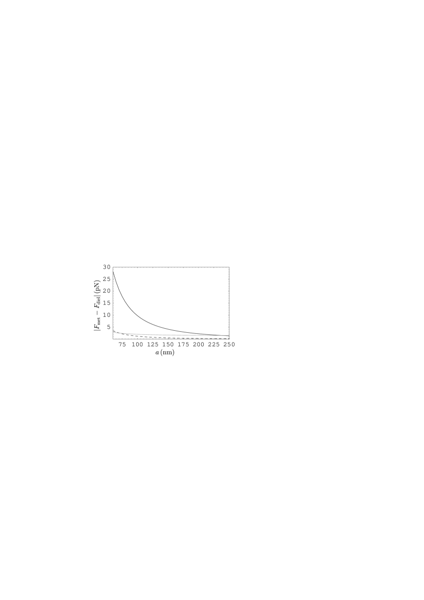
We have also computed the change in the Casimir force predicted by the standard Lifshitz theory, i.e., when is obtained using the dielectric permittivity (the solid line in figure 6) and is obtained using the dielectric permittivity (the dashed line in figure 6). This prediction of the standard theory is shown by the dashed line in figure 8. In this case at separations and 100 nm we obtain and 1.2 pN, respectively. This means that the predictions of the standard Lifshitz theory caused by the change of dielectric permittivity exceed the total experimental error only at the shortest separations below about 70 nm.
4.2 Pressure between an Au plate and a B-doped diamond plate
Here we discuss the possibilities to observe the change of the Casimir pressure in the insulator-metal transition in diamond films using an AFM operated in the dynamic regime. For the dielectric film computations were done with the contribution of free charge carriers omitted (the grey line in figure 6). The obtained Casimir pressure versus separation is shown by the dashed line in figure 9. For a metallic film the dielectric permittivity was used (the solid line in figure 6). In this case the Casimir pressure as a function of separation is presented by the solid line in figure 9. The relative deviations in the Casimir pressure vary from 15.2% and 17.9% at separations 200 and 250 nm, respectively, to 29% at nm.

All the above computations were performed at separations nm where the effect of the phase transition is more pronounced. Qualitatively the same effect, however, takes place at separations of a few nanometers, i.e., in the region of nonretarded van der Waals force. To demonstrate this, we have computed the quantity at , 5, and 10 nm and found that it is equal to 1.9%, 2.0%, and 2.4%, respectively.
We have also calculated the absolute change in the Casimir pressure with the contribution of free charge carriers of the dielectric plate omitted. The computational results are shown by the solid line in figure 10. In the same figure the total experimental error for the difference in Casimir pressures determined at a 67% confidence level is shown by the grey line (the same as in figure 5). As can be seen in this figure, the predicted effect can be easily observed using existing laboratory setup over a wide separation region from 200 to 410 nm. Numerically the calculated change in the Casimir pressure is equal to 38.1, 19.0, 10.7, 6.6, and 4.3 mPa at separations , 250, 300, 350, and 400 nm, respectively. These should be compared with the total error in the pressure difference equal to 3.8 mPa which does not depend on separation in the case of the dynamic AFM [38].

The complete application of the Lifshitz theory, i.e., the use of dielectric permittivities and for dielectric and metallic diamond films, respectively, leads to much smaller changes in the Casimir pressure. They are shown by the dashed line in figure 10. Specifically, at separations and 250 nm the difference computed according to the standard Lifshitz theory is equal to 4.6 and 2.3 mPa, respectively. As can be seen in figure 10, this effect is observable only at the shortest separations ranging from 200 to about 210 nm.
The above computations show that the use of B-doped diamond suggests similar opportunities as the use of Si doped with S or Se with respect to observation of the change in the Casimir force due to the insulator-metal transition. Because of this, choice between the three materials should be done for reasons of convenience in preparation of the test bodies.
5 Conclusions and discussion
In the foregoing we have considered the possible influence of the Mott-Anderson insulator-metal transition in doped semiconductors on the Casimir force and Casimir pressure. This subject was suggested by the unexpected results of several experiments which demonstrated that to bring the measurement data in agreement with computations using the Lifshitz theory one should omit the contribution of free charge carriers in dielectric test bodies. In all the experiments performed to date the dielectric permittivities of a semiconductor plate in the metallic and dielectric states were significantly different. In the proposed experiment using doped semiconductors with high critical concentration of charge carriers, we put forward the possibility to make this difference as small as possible and simultaneously increase the effect from omission of charge carriers in the dielectric state up to the values easily detectable using existing laboratory setups.
We have suggested three different semiconductor materials suitable for use in the proposed esperiment: Si doped with S or Se and diamond doped with B. All these materials offer very prospective opportunities for the observation of the effect under discussion. Thus, for a S-doped Si the calculated difference between the Casimir forces in metallic and dielectric states at separations 60, 100, and 150 nm exceeds the total experimental error by a factor of 9.8, 5.5, and 2.7, respectively. For the Casimir pressures at separations 200, 250, and 300 nm the similar difference in the Casimir pressures exceeds the total experimental error by a factor of 11.9, 6.1, and 3.5, respectively. According to the standard Lifshitz theory the differences between the Casimir forces and pressures in the insulator-metal transition are entirely determined by the differences in the measured dielectric properties of the test bodies. Because of this, the standard Lifshitz theory predicts much smaller changes in the Casimir force and pressure due to insulator-metal transition in S-doped Si. Specifically, for the same concentrations of charge carriers in the dielectric and metallic states, as are used above, the difference in the Casimir forces at separations of 60 and 100 nm exceeds the total experimental error by a factor of 3.7 and 2, respectively. At nm this difference is equal to the total error. The pressure differences computed using the standard Lifshitz theory at , 250, and 300 nm exceed the total experimental error by a factor of 4.4, 2.2, and 1.2, respectively. At nm the total error of the difference in the Casimir pressures exceeds the magnitude of the predicted difference. Thus, theoretical predictions of the two approaches in the experiment proposed differ significantly and their validity can be tested with confidence by comparison with the measurement data.
Finally, we would like to stress that the standard Lifshitz theory does not allow modifications of the Casimir force without change of dielectric permittivity of the test bodies over a wide frequency region. For the case, however, where the contribution of free charge carriers in the dielectric permittivity of the insulating materials should be omitted (as suggested by several experiments discussed in Sec. 1), it becomes possible to achieve significant modifications in the force magnitude with only negligibly small changes in the dielectric permittivity. This happens due to the Mott-Anderson insulator-metal transition in doped semiconductors when the permittivities of insulating and metallic plates differ only slightly. The proposed experiment seems capable of providing definitive answer to the question whether it is possible to modify dispersion forces without change of dielectric permittivity.
References
References
- [1] Parsegian V A 2005 Van der Waals forces: A Handbook for Biologists, Chemists, Engineers, and Physicists (Cambridge: Cambridge University Press)
- [2] Bordag M, Klimchitskaya G L, Mohideen U and Mostepanenko V M 2009 Advances in the Casimir Effect (Oxford: Oxford University Press)
- [3] Buks E and Roukes M L 2001 Phys. Rev. B 63 033402
- [4] Schröder E and Hyldgaard P 2003 Mater. Sci. Engineer. C 23 721
- [5] Schröder E and Hyldgaard P 2003 Surf. Sci. 532-535 880
- [6] Kara A and Rahman T S 2005 Surf. Sci. Rep. 56 159
- [7] Blagov E V, Klimchitskaya G L and Mostepanenko V M 2005 Phys. Rev. B 71 235401
- [8] Blagov E V, Klimchitskaya G L and Mostepanenko V M 2007 Phys. Rev. B 75 235413
- [9] Bimonte G, Calloni E, Esposito G, Milano L and Rosa L 2005 Phys. Rev. Lett. 94 180402
- [10] Bimonte G, Calloni E, Esposito G and Rosa L 2005 Nucl. Phys. B 726 441
- [11] Bezerra V B, Klimchitskaya G L, Mostepanenko V M and Romero C 2010 Phys. Rev. D 81 055003
- [12] Bezerra V B, Klimchitskaya G L, Mostepanenko V M and Romero C 2011 Phys. Rev. D 83 075004
- [13] Mostepanenko V M, Bezerra V B, Klimchitskaya G L and Romero C 2011 Int. J. Mod. Phys. A 27 1260015
- [14] London F 1930 Z. Phys. 63 245
- [15] Casimir H B G 1948 Proc. K. Ned. Akad. Wet. B 51 793
- [16] Langreth D C, Dion M, Rydberg H, Schröder E, Hyldgaard P and Lundqvist B I 2005 Int. J. Quant. Chem. 101 599
- [17] Lifshitz E M 1956 Zh. Eksp. Teor. Fiz. 29 94 (1955 Sov. Phys. JETP 2 73)
- [18] Lifshitz E M and Pitaevskii L P 1984 Statistical Physics, Pt II (Oxford: Pergamon Press)
- [19] Emig T, Jaffe R L, Kardar M and Scardicchio A 2006 Phys. Rev. Lett. 96 080403
- [20] Emig T, Graham N, Jaffe R L and Kardar M 2007 Phys. Rev. Lett. 99 017403
- [21] Kenneth O and Klich I 2008 Phys. Rev. B 78 014103
- [22] Bimonte G, Emig T, Jaffe R L and Kardar M 2012 Europhys. Lett. 97 50001
- [23] Bimonte G, Emig T and Kardar M 2012 Appl. Phys. Lett. 100 074110
- [24] Klimchitskaya G L, Mohideen U and Mostepanenko V M 2009 Rev. Mod. Phys. 81 1827
- [25] Klimchitskaya G L, Mohideen U and Mostepanenko V M 2011 Int J. Mod. Phys. B 25 171
- [26] Rodriguez A W, Capasso F and Johnson S G 2011 Nature Photon. 5 211
- [27] Chiu H-C, Klimchitskaya G L, Marachevsky V N, Mostepanenko V M and Mohideen U 2009 Phys. Rev. B 80 121402(R)
- [28] Chiu H-C, Klimchitskaya G L, Marachevsky V N, Mostepanenko V M and Mohideen U 2010 Phys. Rev. B 81 115417
- [29] Chang C-C, Banishev A A, Klimchitskaya G L, Mostepanenko V M and Mohideen U 2011 Phys. Rev. Lett. 107 090403
- [30] Banishev A A, Chang C-C, Castillo-Garza R, Klimchitskaya G L, Mostepanenko V M and Mohideen U 2012 Phys. Rev. B 85 045436
- [31] Banishev A A, Chang C-C, Klimchitskaya G L, Mostepanenko V M and Mohideen U 2012 Phys. Rev. B 85 195422
- [32] Decca R S, Fischbach E, Klimchitskaya G L, Krause D E, López D and Mostepanenko V M 2003 Phys. Rev. D 68 116003
- [33] Decca R S, López D, Fischbach E, Klimchitskaya G L, Krause D E and Mostepanenko V M 2005 Ann. Phys. NY 318 37
- [34] Decca R S, López D, Fischbach E, Klimchitskaya G L, Krause D E and Mostepanenko V M 2007 Phys. Rev D 75 077101
- [35] Decca R S, López D, Fischbach E, Klimchitskaya G L, Krause D E and Mostepanenko V M 2007 Eur. Phys. J. C 51 963
- [36] Boström M and Sernelius B E 2000 Phys. Rev. Lett. 84 4757
- [37] Chang C-C, Banishev A A, Castillo-Garza R, Klimchitskaya G L, Mostepanenko V M and Mohideen U 2012 Phys. Rev. B 85 165443
- [38] Chang C-C, Banishev A A, Castillo-Garza R, Klimchitskaya G L, Mostepanenko V M and Mohideen U 2012 Int. J. Mod. Phys.: Conf. Ser. 14 270
- [39] Masuda M and Sasaki M 2009 Phys. Rev. Lett. 102 171101
- [40] Sushkov A O, Kim W J, Dalvit D A R and Lamoreaux S K 2011 Nature Phys. 7 230
- [41] Bezerra V B, Klimchitskaya G L, Mohideen U, Mostepanenko V M and Romero C 2011 Phys. Rev. B 83 075417
- [42] Klimchitskaya G L, Bordag M, Fischbach E, Krause D E and Mostepanenko V M 2011 Int. J. Mod. Phys. A 26 3918
- [43] Klimchitskaya G L, Bordag M and Mostepanenko V M 2012 Int. J. Mod. Phys. A 27 1260012
- [44] Garcia-Sanches D, Fong K Y, Bhaskaran H, Lamoreaux S and Tang H X 2012 Phys. Rev. Lett. 109 027202
- [45] Bordag M, Klimchitskaya G L and Mostepanenko V M 2012 arXiv:1208.1757v1
- [46] Chen F, Klimchitskaya G L, Mostepanenko V M and Mohideen U 2007 Optics Express 15 4823
- [47] Chen F, Klimchitskaya G L, Mostepanenko V M and Mohideen U 2007 Phys. Rev. B 76 035338
- [48] Obrecht J M, Wild R J, Antezza M, Pitaevskii L P, Stringari S and Cornell E A 2007 Phys. Rev. Lett. 98 063201
- [49] Klimchitskaya G L and Mostepanenko V M 2008 J. Phys. A: Math. Theor. 41 312002
- [50] Banishev A A, Chang C-C, Castillo-Garza R, Klimchitskaya G L, Mostepanenko V M and Mohideen U 2012 Int. J. Mod. Phys. A 27 1260001
- [51] Bezerra V B, Klimchitskaya G L and Mostepanenko V M 2002 Phys. Rev. A 66 062112
- [52] de Man S, Heeck K, Wijngaarden R J and Iannuzzi D 2009 Phys. Rev. Lett. 103 040402
- [53] de Man S, Heeck K and Iannuzzi D 2010 Phys. Rev. A 82 062512
- [54] Geyer B, Klimchitskaya G L and Mostepanenko V M 2005 Phys. Rev. D 72 085009
- [55] Mostepanenko V M and Klimchitskaya G L 2010 Int. J. Mod. Phys. A 25 2302
- [56] Shklovskii B I and Efros A L 1984 Electronic Properties of Doped Semiconductors. Solid State Series, v.45 (Berlin: Springer)
- [57] Tomaš M S 2002 Phys. Rev. A 66 052103
- [58] Chen F, Klimchitskaya G L, Mostepanenko V M and Mohideen U 2006 Phys. Rev. Lett. 97 170402
- [59] Rosenbaum T F, Milligan R F, Paalanen M A, Thomas G A, Bhatt R N and Lin W 1983 Phys. Rev. B 27 7509
- [60] Dai P, Zhang Y and Sarachik M P 1991 Phys. Rev. Lett. 66 1914
- [61] Winkler M T, Recht D, Sher M-J, Said A J, Mazur E and Aziz M J 2011 Phys. Rev. Lett. 106 178701
- [62] Ertekin E, Winkler M T, Recht D, Said A J, Aziz M J, Buonassisi T and Grossman J C 2012 Phys. Rev. Lett. 108 026401
- [63] Klein T, Achatz P, Kacmarcik J, Marcenat C, Gustafsson F, Marcus J, Bustarret E, Pernot J, Omnes F, Sernelius Bo E, Persson C, Ferreira da Silva A and Cytermann C 2007 Phys. Rev. B 75 165313
- [64] Palik E D (ed) 1991 Handbook of Optical Constants of Solids, vol 2 (New York: Academic)
- [65] Lambrecht A, Pirozhenko I, Duraffourg L and Andreucci Ph 2007 Europhys. Lett. 77 44006
- [66] Palik E D (ed) 1985 Handbook of Optical Constants of Solids, vol 1 (New York: Academic)
- [67] Bimonte G 2011 Phys. Rev. A 83 042109
- [68] Bergström L 1997 Adv. Coll. Interface Sci. 70 125
- [69] Ortolani M, Lupi S, Baldassarre L, Schade U, Calvani P, Takano Y, Nagao M, Takenouchi T and Kawarada H 2006 Phys. Rev. Lett. 97 097002