Buried heterostructure vertical-cavity surface-emitting laser with semiconductor mirrors
Abstract
We report a buried heterostructure vertical-cavity surface-emitting laser fabricated by epitaxial regrowth over an InGaAs quantum well gain medium. The regrowth technique enables microscale lateral confinement that preserves a high cavity quality factor (loaded 4000) and eliminates parasitic charging effects found in existing approaches. Under optimal spectral overlap between gain medium and cavity mode (achieved here at = 40 K) lasing was obtained with an incident optical power as low as = 10 mW ( = 808 nm). The laser linewidth was found to be 3 GHz at 5 .
pacs:
42.60.By, 42.55.Sa, 42.55.Px, 42.60.DaSince their inception, iga1988ses vertical-cavity surface-emitting lasers (VCSELs), have dramatically improved in terms of speed,anan2007pis efficiency,amann2012eeh and output power,higuchi2012hpd and are now widely available commercially. One of the principle advantage of VCSELs is a scalable production process, but VCSELs also feature continuous single-mode operation, huffaker1994nod ; ohiso2002sto mode-hop free tuning, changhasnain2000tvc and improved beam qualitygustavsson2006def compared to edge emitting devices. Nevertheless, reducing VCSEL dimensions into the nanoscale has proved challenging, despite being of great interest for future integration of optics and microelectronics. Three-dimensionally confining heterostructures have demonstrated progress in this direction, including electrically-pumped room-temperature operation,zhou2000eis but under size reduction these structures are expected to suffer parasitic carrier loss associated with etched and exposed interfaces. A fully-buried heterostructure gain structure has the potential to dramatically improve VCSEL performance by eliminating such parasitic charging effects in the perimeter region of the VCSEL s gain material. The buried heterostructure (BH) is expected to produce lower threshold, higher efficiency, and higher modulation speed for microscale VCSEL devices. In addition, improved current funneling and heat dissipation in a BH VCSEL may permit operation further above threshold and consequently lead to a further reduction in the laser linewidth.kim2012nlo For sensing applications a narrow linewidth is essential for reaching higher resolution. However, because VCSEL performance is also strongly dependent on cavity loss, a BH VCSEL requires a design that can also form a high quality factor microcavity. Although there has been rapid progress in the development of microcavity technology in recent years, vahala2003om buried heterostructure designs have typically been non-epitaxial.ohiso2001bhv
Here we report a BH quantum well VCSEL in which the epitaxial cavity is overgrown on the active material rather than on the perimeter of the semiconductor cavity.iga1988ses ; changhasnain1993ltb We describe the design, surface topography, and optical characteristics of devices based on lithographically defined mesas with a diameter as small as 3 m. We find that under optimal spectral overlap lasing is observed with a threshold power of the same order as that of ordinary VCSELs.disopra1999niv High-resolution measurements with a scanning Fabry-Perot interferometer reveal a laser linewidth of several GHz just above threshold.
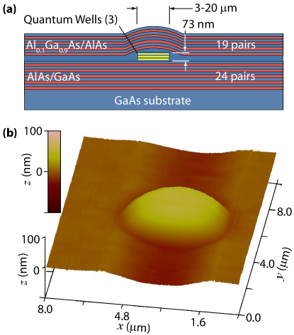
Our devices were grown by molecular beam epitaxy (MBE) on a GaAs substrate [Fig. 1(a)]. A lower distributed Bragg reflector (DBR) consisting of 24 GaAs/AlAs quarter-wave pairs served as the bottom mirror onto which a gain region of 3 InGaAs quantum wells was grown. Arrays of mesas with diameters ranging from 3 m to 20 m and with a height of 73 nm were defined in this gain region by ultraviolet lithography and subsequent wet etching. A final HF etch was used prior to reloading the sample in the growth system. The top DBR, consisting of 19 Al0.1Ga0.9As/AlAs quarter-wave pairs, was grown over the etched mesa. The regrowth process is derived from methods developed in prior work using a semiconductor quantum dot gain medium.lu2005lsa ; muller2006hqa
The surface topography of our overgrown sample was obtained by atomic force microscopy (AFM). As seen in Fig. 1(b) for a cavity based on a 3 m diameter mesa, the overgrown surface assumes the shape of a convex lens, with a height close to that of the mesa from which it originates. The lens in Fig. 1(b) is actually slightly elongated in the direction with an aspect ratio of 1.3 due to anisotropic epitaxial growth. The cross-section of the lens of Fig. 1(b) along the direction is shown in Fig. 2(a).
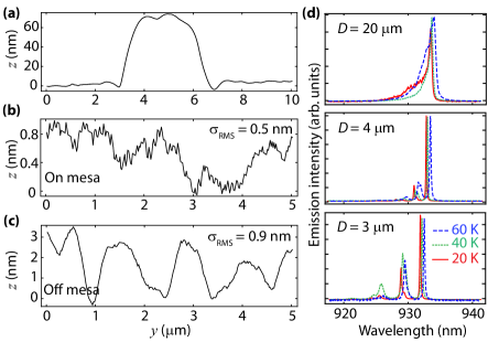
An essential requirement of the regrowth process is a high surface quality so that scattering losses are minimized. A simple estimate of required root-mean-square (RMS) surface microroughness, , can be obtained using Ruze’s equation, , which provides an expression for mirror scattering loss, , at a given wavelength.ruze1952 For a Fabry-Perot cavity of length , the cavity quality factor, , is related to the total cavity round trip loss, , through the expression . Therefore, for a cavity that is about one wavelength long, the maximum microroughness that can be tolerated to sustain a quality factor , is estimated as . Thus, in the present case, for 5000 we must have 0.8 nm. AFM linescans in Fig. 2(b) and (c) show a zoomed in measurement on, and off a (80100 m) mesa location, respectively. The corresponding root-mean-square surface microroughness is = 0.5 nm and = 0.9 nm, respectively, revealing a smooth overgrowth compatible with a quality factor on the order of 5000 or larger.
Normalized photoluminescence (PL) spectra of structures based on mesas with diameters of 20 m, 4 m, and 3 m are shown in Fig. 2(d). The wavelength of the pump laser was = 808 nm. With decreasing mesa diameter the spectra clearly reveal an increase in the spectral separation of the microcavity resonances, accompanied by a blue shift due to the increased lateral confinement.
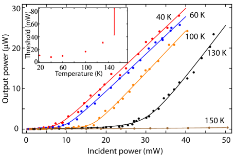
Laser oscillation was investigated using the same experimental configuration as that for PL, but applying a higher pump power. Figure 3 shows the output power versus incident pump power for a BH VCSEL based on a 3 m mesa at temperatures ranging from 40 K to 150 K. The extracted threshold is plotted in the inset versus temperature, with a minimum threshold measured near 40 K. This temperature corresponds to the designed value for the spectral gain offset. Lasing is obtained up to 130 K within the range of available input power. This upper temperature limit is set by detuning of the quantum well gain peak away from the cavity resonance. Note that the threshold powers given here are those of the 808 nm laser at the input of our cryostat. The actual threshold power is significantly lower when one accounts for the light reflected and scattered by the upper DBR and the small absorption path of the quantum well gain region, in addition to losses incurred by one lens, two windows, and one mirror.
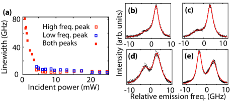
Figure 4 shows more details of the lasing properties for the 3 m BH VCSEL. In Fig. 4(a) the linewidth of the lowest order transverse mode [rightmost peak in bottom panel of Fig. 2(d)] is shown as a function of incident pump power. Measurements were performed with a grating spectrometer with a resolution 20 GHz and with a scanning Fabry-Perot interferometer with a resolution of 35 MHz. Pump powers up to 6 times the threshold power were used. The linewidth measurements far below threshold indicate that the 3 m cavity has a quality factor of 4000. This quality factor is that of the loaded cavity subject to significant absorption due to the three quantum wells. It cannot be compared directly to cavity quality factors measured with no gain medium akahane2003hpn or a gain medium consisting of a single layer of InAs quantum dots.muller2006hqa ; stoltz2005hqf Substantial narrowing is measured above threshold, with a linewidth of about 3 GHz for the highest power. The high resolution spectra [Fig. 4(b-e)] also reveal a splitting of the lowest order transverse mode into two peaks of perpendicular polarization. As is seen in the panels in which the pump power is increased from 8.5 mW [Fig. 4(b)] to 22.6 mW [Fig. 4(e)], one of the peaks reaches threshold first.
In summary, we have presented an all-epitaxial BH VCSELs using quantum well gain regions. The buried approach provides the possibility of scaling the VCSEL to smaller sizes without suffering parasitic carrier losses. The sample described here was optimized for low-temperature operation in order to relax requirements on pump laser performance. However, next steps will aim at extending operation to room temperature and to electrical pumping. Future efforts will further focus on reducing the BH VCSEL to smaller diameters of order 1 m.
This work is supported by the Army Research Office under Grant No. W911NF-12-1-0046.
References
- (1) K. Iga, F. Koyama, and S. Kinoshita, IEEE J. Quantum Electron. 24, 1845 (1988).
- (2) T. Anan, in Proc. International Symposium on VCSELs and Integrated Photonics, E3 (2007).
- (3) M.-C. Amann, E. Wong, and M. Mueller, in Proc. Optical Fiber Communication Conference (OFC), OTh4F (2012).
- (4) A. Higuchi, H. Naito, K. Torii, M. Miyamoto, J. Maeda, H. Miyajima, and H. Yoshida, Optics Express 20, 4206 (2012).
- (5) D. L. Huffaker, D. G. Deppe, K. Kumar, and T. J. Rogers, Appl. Phys. Lett. 65, 97 (1994).
- (6) Y. Ohiso, H. Okamoto, R. Iga, K. Kishi, and C. Amano, IEEE Photon. Tech. Lett. 14, 738 (2002).
- (7) C. J. Chang-Hasnain, IEEE Sel. Top. Quantum Electron. 6, 978 (2000).
- (8) A. Haglund, J.S. Gustavsson, J Bengtsson, P. Jedrasik, A. Larsson, IEEE J. Quantum Electron. 42, 231 (2006).
- (9) W. D. Zhou, J. Sabarinathan, B. Kochman, E. Berg, O. Qasaimeh, S. Pang, and P. Bhattacharya, Electron. Lett. 36, 1541 (2000).
- (10) Y. Ohiso, H. Okamoto, R. Iga, K. Kishi, K. Tateno, and C. Amano, IEEE J. Quantum Electron. 37, 1194 (2001).
- (11) F. M. di Sopra, H. P. Zappe, M. Moser, R. Howel, H. P. Gauggel, and K. Gulden, IEEE Photon. Technol. Lett. 11 1533 (1999).
- (12) J. Kim, A. Shinya, K. Nozaki, H. Taniyama, C.-H. Chen, T. Sato, S. Matsuo, and M. Notomi, Optics Express 20, 11643 (2012).
- (13) K. J. Vahala, Nature 424, 839 (2003).
- (14) C. J. Chang-Hasnain, Y. A. Wu, G. S. Li, G. Hasnain, K. D. Choquette, C. Caneau, and L. T. Florez, Appl. Phys. Lett. 63, 1307 (1993).
- (15) D. Lu, J. Ahn, S. Freisem, and D.G. Deppe, Appl. Phys. Lett. 87, 163105 (2005).
- (16) A. Muller, C.K. Shih, J. Ahn, D. Lu, D. Gazula, and D.G. Deppe, Appl. Phys. Lett. 88, 031107 (2006).
- (17) J. Ruze, Nuevo Cimento Suppl. 9, 364 (1952).
- (18) Y. Akahane, T. Asano, B.-S. Song, and S. Noda, Nature 425, 944 (2003).
- (19) N. G. Stoltz, M. Rakher, S. Strauf, A. Badolato, D. D. Lofgreen, P. M. Petroff, L. A. Coldren, and D. Bouwmeester, Appl. Phys. Lett. 87, 031105 (2005).