Giant Faraday effect due to Pauli exclusion principle in 3D topological insulators
Abstract
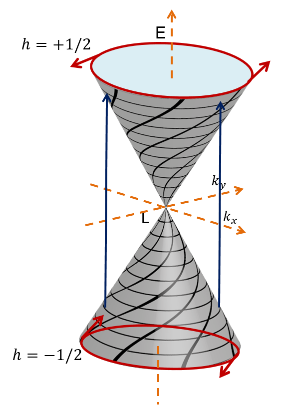
Experiments using ARPES, which is based on the photoelectric effect, show that the surface states in 3D topological insulators (TI) are helical. Here we consider Weyl interface fermions due to band inversion in narrow-bandgap semiconductors, such as Pb1-xSnxTe. The positive and negative energy solutions can be identified by means of opposite helicity in terms of the spin helicity operator in 3D TI as , where is a Dirac matrix and points perpendicular to the interface. Using the 3D Dirac equation and bandstructure calculations we show that the transitions between positive and negative energy solutions, giving rise to electron-hole pairs, obey strict optical selection rules. In order to demonstrate the consequences of these selection rules, we consider the Faraday effect due to Pauli exclusion principle in a pump-probe setup using a 3D TI double interface of a PbTe/Pb0.31Sn0.69Te/PbTe heterostructure. For that we calculate the optical conductivity tensor of this heterostructure, which we use to solve Maxwell’s equations. The Faraday rotation angle exhibits oscillations as a function of probe wavelength and thickness of the heterostructure. The maxima in the Faraday rotation angle are of the order of millirads.
pacs:
78.67.-n,78.67.Hc,78.67.Wj,71.15.MbI Introduction
The 3D TI is a new state of matter on the surface or at the interface of narrow-bandgap materials where topologically protected gapless surface/interface states appear within the bulk insulating gap.key-1 ; key-2 ; key-11 ; Hsieh:2009 ; Hajlaoui:2012 ; key-6-1 ; key-7-1 ; key-5-1 These states are characterized by the linear excitation energy of massless Weyl fermions. The spins of the Kramers partners are locked at a right angle to their momenta due to the Rashba spin-orbit coupling,key-21-1 protecting them against perturbation and scattering.key-1 ; key-2 ; key-3 ; key-4 Because of the presence of a single Dirac cone with fixed spin direction at the surface, the main feature of strong TIs,key-8 ; key-9 the materials Bi2Se3 and Bi2Te3 are currently being widely studied.key-10 ; key-11 ; key-5-1
The heterostructures of compound semiconductors such as Bi1-xSbx and Pb1-xSnxTe exhibit a strong topological phase.key-4 In Bi1-xSbx, the and bands cross at . The pure PbTe has inverted bands at the band gap extrema with respect to SnTe. In Pb1-xSnxTe, initially increasing the concentration of Sn leads to a decreasing band gap. At around , the bands cross and the gap reopens for with even parity band and odd parity band being inverted with respect to each other.key-12 The band inversion between PbTe and SnTe results in interface states,key-13 ; key-14 ; key-15 which can be described by the Weyl equation.key-16
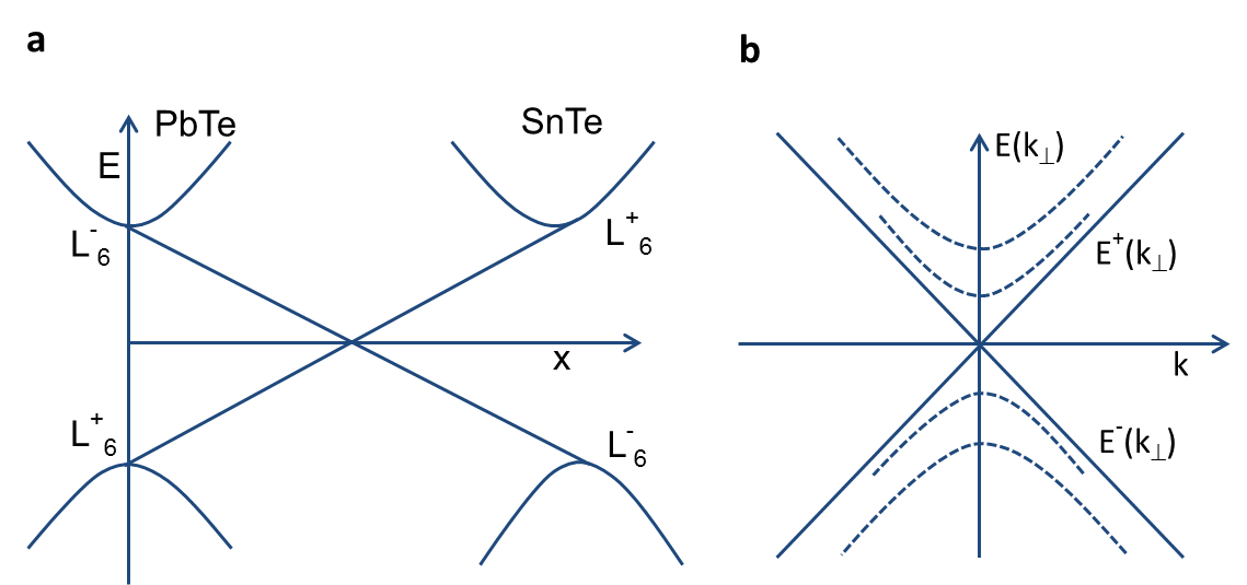
Here we investigate the giant Faraday effect due to Pauli exclusion principle and the strict optical selection rules governing the low energy excitation of electron-hole pairs around a Dirac point in a 3D TI. Due to interference effects, the Faraday rotation angle exhibits oscillations as a function of probe wavelength and thickness of the slab material on either side of the 3D TI double interface of a PbTe/Pb0.31Sn0.69Te/PbTe heterostructure. The maxima in the Faraday rotation angle are in the mrad regime. We find that in 3D TIs both interband transitions (between positive and negative energy solutions) and intraband transitions (within the same energy solutions) are allowed. Note that the selection rules obtained here are different from the selection rules in ARPES experiments, which record the number of photoelectrons as a function of kinetic energy and emission angle with respect to the sample surface. A number of experiments have shown the existence of the helical surface states in 3D TI.key-10 ; key-11 As an example, we consider the alloy Pb1-xSnxTe, which has topologically nontrivial interface states under appropriate doping level. Our results are qualitatively valid for all strong 3D TIs. Pb1-xSnxTe has a rocksalt type crystal lattice with four non-equivalent L points located in the center of the hexagonal facets on [111] axis. The valence and conduction band edges are derived from the hybridized p-type and s-type orbitals at the point.key-17 Its end species have inverted band character, character of PbTe band switches to character of SnTe band and vice versa as shown in Fig. 1. The Brillouin zone of the Pb1-xSnxTe crystal has eight hexagonal faces each with center at the point. Two faces lying diametrically opposite are equivalent. As a result, the band inversion happens at four distinct Dirac points. The crystal possesses a mirror symmetry. Therefore, it is a distinct class of 3D TI where surface states are protected by mirror symmetry.Hasan We choose the -axis to point in direction of the gradient of the concentration . At the two band extrema, the low energy Hamiltonian is described by a 3D relativistic Dirac equation whose solutions are localized near the plane where the band crossing occurs, which defines the interface. Dispersion is nearly linear owing to the large band velocities of m/s and m/s with a small gap.key-16 Such properties result in a small localization length of the interface wave functions along the -axis. Due to the absence of a center of inversion, a Rashba-type spin-orbit coupling is present, which is automatically taken into account through the Dirac equation. We also present the details of our ab-initio calculation of the bandstructure in the supercell Brillouin zone obtained by doubling the lattice parameters in each direction. Analysis of the alloy band structures is usually complicated due to folding of the bands from neighboring Brillouin zones, making it difficult to map the calculated bandstructures onto the bandstructures obtained from momentum-resolving experiments. The analysis is further complicated by the presence of impurity bands inside the normal bulk energy gap. The interface states sometimes overlap with bulk energy states. Therefore, we unfold the band structures along the [111] direction in order to shift the band crossing from the point, as seen in the supercell Brillouin zone, to the point in the primitive cell Brillouin zone.key-18 ; key-19
We developed a method of the Faraday rotation of a single photon due to Pauli exclusion principle for a topologically trivial quantum dotLeuenberger:2005 ; Leuenberger:2006 and for a 3D TI quantum dot.Paudel:2013 The proposed method can be used for entangling remote excitons, electron spins, and hole spins. We showed that this entanglement can be used for the implementation of optically mediated quantum teleportation and quantum computing.
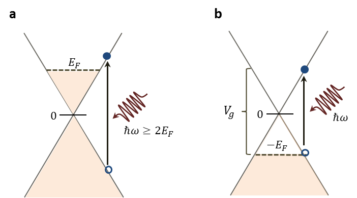
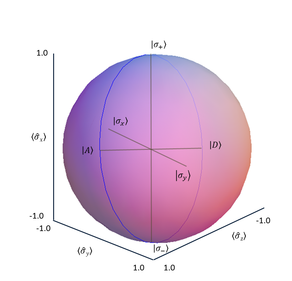
Here we investigate the Faraday effect due to the Pauli exclusion principle for a 3D TI double interface of a PbTe/Pb0.31Sn0.69Te/PbTe heterostructure. This Faraday effect is completely different from the Faraday effect due to an external magnetic field, which was presented in Ref. TseMacDonald, for a thin film of a 3DTI where a gap was opened by breaking the time reversal symmetry through a magnetic field. The Faraday effect presented here arises from the polarization of electron-hole (e-h) pairs that are excited by means of a linearly polarized laser pump beam. A laser probe beam with energy below twice the absolute value of the Fermi energy measured from the Dirac point cannot be absorbed due to the absence of charge carriers in this energy regime. The excitation of the Weyl fermion can happen when a photon has an energy of as shown in the Fig. 3a. There are no interband transitions with the photon energy less than . A gate voltage can also be applied to shift the Fermi level below the Dirac nodeKim . Fig. 3b shows the scheme of the gate-induced shift in the Fermi level. In the Figure photon of energy can excite a Weyl fermion. We call this energy regime the transparency region, in order to avoid confusion with a bandgap in a gapped semiconductor material. When - and -linearly polarized e-h pairs are present, a probe beam linearly polarized along the diagonal direction experiences a Faraday rotation on the Poincare sphere as shown in Fig. 9. The resulting Faraday rotation angle is giant and of the order of mrad. It exhibits oscillations as a function of the slab thickness of the two PbTe layers of the PbTe/Pb0.31Sn0.69Te/PbTe heterostructure containing two interfaces (see Fig. 8). The Pb0.31Sn0.69Te is 10 nm thick in order to introduce a gap for three out of the four L-points, as described below. The Faraday effect results then only from the excitation of e-h pairs at a single L-point.
The paper is organized as follows. In Sec. II we present the analytical derivation of the Weyl solution of the Dirac equation that describes the level crossing at the point. Using the Rashba spin-orbit Hamiltonian, we derive the helicity operator for 3D topological insulators in Sec. III. Sec. IV is devoted to the evaluation of the optical transition matrix elements. The resulting optical selection rules are discussed in Sec. IV. In order to obtain a quantitative result for the optical transition matrix elements, we perform a bandstructure calculation of the alloy Pb1-xSnxTe in Sec. V. The Sec.VI is devoted to the explicit derivation of the Faraday rotation effect and calculation of the Faraday rotation angle in the PbTe/Pb0.31Sn0.69Te/PbTe heterostructure.
II Model based on Dirac equation
The energy spectrum of Pb1-x SnxTe near the band crossing is described within the perturbation theory by the two-band Dirac HamiltonianNimtz:1983
| (1) |
where are the Pauli matrices, is the momentum operator and is the gap energy parameter with symmetry . and denote the Pauli matrices and momenta in the interface plane, respectively. The transverse and longitudinal velocities are determined by and , where and are the transverse and longitudinal Kane interband matrix elements, respectively. kg is the free electron mass. The inhomogeneous structure is synthesized by changing the composition along one of the [111] axes, whose symmetry breaking leads to a single Dirac cone in the chosen direction,key-23-1 thereby recovering the Z2 strong topological insulator phase. The direction of the gradient of the concentration defines our -axis. After the unitary transformation of the Hamiltonian using
| (2) |
the time-independent Dirac equation can be written as
| (5) | |||
| (10) |
where and are the two-component spinors of the and the band, respectively. The potential (work function) describes the variation of the gap center. For simplicity we consider the case . From Eq. (10), the two-component spinor satisfies
| (11) |
where . In its origin, the linear Weyl spectrum at is approximately equal to the soliton spectrum in the 1D Peierl’s insulator. This implies that can be chosen to be . Interface states are localized along the -axis with the localization length . For , additional branches with finite mass appear. There are several solutions at which are localized at the contact. For , only Weyl solutions exist. We focus on the case when . Then we have only zero-energy solutions, which correspond to the Weyl states and are given by key-16
| (12) |
where C is a normalization constant, and . These solutions have eigenenergies . For to vanish at the inverted contact, it can be seen from Eq. (10) that and must have only non-zero spin down and spin up components, respectively. Each spinor at band can be represented with the spin up states from the band and spin down states from the band for both the positive and the negative energies. The motion of the particle at the inverted contact is separated into free motion in the -plane and confinement along the -axis. A remarkable property of Eq. (10) is the presence of the zero mode (Weyl mode) localized around . It is this mode that has a locked spin structure. In order to understand the direction in which the 4-spinors point, we have to transform the solutions back to the original basis of the Hamiltonian in Eq. (1). After the back transformation , the Weyl solutions are
| (13) |
where C is a normalization constant. These solutions have eigenenergies and are helical. At this time, it is useful to introduce the notation
| (14) |
where is the four-spinor consisting of the two-spinors and are two-spinors, and . We define .
III Helicity operator
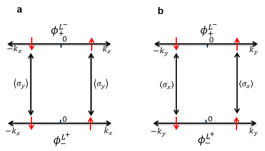
We show in this section that it is possible to clearly identify the positive and negative energy solutions by means of a spin helicity operator. In the representation shown in Eq. (14), the spin directions reveal themselves clearly: the spins of the two-spinors and point perpendicular to owing to the shifts. For an asymmetric scalar potential applied to a semiconductor heterostructure, the inversion symmetry is broken, which leads to the Rashba spin-orbit coupling.key-21-1 ; key-20 Here in the case of the interface of a 3D TI we have antisymmetric potentials , which correspond to the diagonal elements of the Hamiltonian and whose signs depend on the band . This results in a band-dependent Rashba spin-orbit coupling. For the positive (negative) solutions the Rashba spin-orbit coupling has the form , ( sign for positive energy solutions and sign for negative energy solutions), where is the Rashba spin-orbit coupling constant. It is to be noted that in both cases each spin is perpendicular both to the momentum and to the potential gradient direction, i.e. the -axis (see Fig. 4). Our findings are consistent with the spin density functional calculations (DFT).key-22
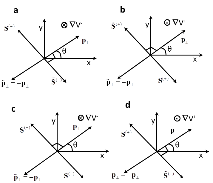
In order to determine the Kramers partners explicitly, we rotate the phase of each of the two-spinor wavefunction by an angle in the 2D interface plane, yielding and . Their spin and momentum direction are flipped by an angle (Fig. 4). This provides a theoretical hallmark of Kramers partners in 3D TI.
Helical properties of solutions given by Eq. (13) apply to all 3D TIs. In the case of free neutrinos in 3D space, the standard helicity operator for the spin can be used. Similarly, in the case of graphene the helicity for the pseudospin is given by . However, in the case of 3D TI this definition is not useful, because the spin points perpendicular to the momentum. Therefore, since we know that the Rashba spin-orbit coupling is responsible for the helicity in 3D TIs, we define the 3D TI helicity operator as
| (17) | |||||
| (18) |
where is the 2D vector of Pauli matrices in the -plane and is a Dirac matrix. Note that the and signs in front of the diagonal terms are due to the direction of and thus a direct consequence of the Rashba spin-orbit coupling. The eigenfunctions of the operator are the 4-spinor wavefunctions given by the Eq. (13) with the eigenvalues for the positive energy solution and for the negative energy solution, i.e. . commutes with the Hamiltonian in Eq. (1). This provides the possibility to write an effective 2D Hamiltonian for the Weyl fermions on the surface of 3D topological insulators, i.e.
| (19) |
This effective 2D Hamiltonian can be reduced to two Weyl Hamiltonians of the form . It is important to note that both 2-spinors of , the 2-spinor of the band and the 2-spinor of the band have the same helicity, in contrast to the commonly used Weyl Hamiltonians . The reason for this is that the two 2-spinors are coupled through the mass term in -direction, as given in the 3D Hamiltonian in Eq. (1).
IV Optical transition matrix elements
We calculate the low-energy transitions around the valley that is lifted up along the -direction from the other three valleys. With the proper choice of uniform strain, composition and layer width, there exist practically gapless helical states for the [111] valley inside the gapped states of the oblique valleys.key-23-1 In unstrained Pb1-xSnxTe, band inversion occurs simultaneously at four points and the phase is topologically trivial. For most experiments, in a structure with a layer of thickness d nm between the two interfaces in a PbTe/Pb0.31Sn0.69Te/PbTe heterostructure, dispersion of the [111] valley states can be assumed to be gapless while the states in the oblique valleys are gapped.key-23-1 The interface can be modeled with the bulk of Pb0.31Sn0.69Te and PbTe with bandgaps of, respectively, -0.187 and 0.187 eV, so that Weyl fermions are generated at the two interfaces. Here, the bandgap formula provided in Ref. Yusheng, was used. It is to be noted that localized spin states of 2D Weyl fermions in 3D TI are solutions of the Hamiltonian given in Eq. (1).
Now we proceed to calculate the optical selection rules for the excitation of electron-hole pairs, keeping in mind that the Dirac equation provides an effective description of the two-band system consisting of the bands. The Hamiltonian contains also a quadratic term in the momenta,Nimtz:1983 namely
| (20) |
where and are the longitudinal and transverse effective masses of the bands, respectively. Through minimal coupling the quadratic term leads to a linear term in the momentum, which we need to take into account. Hence, in the presence of electromagnetic radiation, the total Hamiltonian for the Dirac particle is given by
| (23) | |||||
where is the vector potential, and are the Dirac matrices , , and in the Coulomb gauge. We identify the interaction Hamiltonian as
| (24) | ||||
| (27) |
It will turn out that only interband transitions contribute for a 2D interface, whereas both interband and intraband transitions contribute in the case of a 3DTI quantum dot. It is important to note that and include the Kane interband matrix elements , where are the Bloch’s functions for the bands. This means that the interband transitions are governed by the interband Hamiltonian , where the Dirac - matrices couple the band with the band. The Hamiltonian accounts for intraband transitions with operating on the envelope wavefunctions only. is proportional to the identity in 4-spinor space and therefore couples the band to itself and the band to itself. Thus the interband Hamiltonian and the intraband Hamiltonian are not equivalent in this description. On the one hand, gives rise to interband transitions because it contains the Kane interband matrix elements and . On the other hand, gives rise to intraband transitions because the term operates on the envelope wavefunctions.
We start with calculating the interband matrix elements which are given by the off diagonal elements of the interaction Hamiltonian. We identify and as the longitudinal and transverse relativistic current densities, respectively. Therefore, the evaluation of the optical transition matrix elements is reduced to calculating the matrix elements of .
The optical transition matrix elements involve the integral over the envelope functions and the periodic part of the Bloch functions. The integral over the envelope function can be carefully separated out from the remaining part, similarly to the case of wide-bandgap semiconductor materials.Yu&Cardona The idea is to separate the slowly varying envelope part from the rapidly varying periodic part of the total wavefunction. For that we need to first replace the position vector by , where is a lattice vector and is a vector within one unit cell. Writing the vector potential and taking advantage of the periodicity and the fact that , we obtain
| (28) | |||||
for an optical transition from the initial state to the final state . is the volume of the unit cell. By applying the secular approximation to the term with the exponential function , we obtain , which ensures momentum conservation in the plane of the interface. Using the normalization , the optical matrix element is well approximated by
| (29) | |||||
Note that in contrast to semiconductor quantum wells where the overlap between electron and hole envelope wavefunctions is smaller than 1 in general, here the overlap between Weyl envelope wavefunctions is . We assume that the wavelength of incoming photon is small compared to the lattice constant. This means we can use the dipole approximation: . Since there is no net momentum transfer the directions of the initial and final momentum vectors are the same; i.e. we consider only vertical transitions. For the matrix elements we obtain the following interband matrix elements:
| (30) |
These transitions are vertical. The z-component of the matrix element of vanishes.
The Kane interband matrix element can be calculated explicitly. The periodic function can be written as , where is the reciprocal lattice vector and are the expansion cofficients for the bands. The Kane interband matrix elements can be evaluated as
| (31) |
For the vertical transitions and , we obtain
| (32) |
The diagonal matrix elements of the interaction Hamiltonian give rise to the intraband transitions. As stated above, the intraband matrix elements operate on the envelope functions only and thus couple to the band to itself and band to itself. In the electric dipole approximation the transitions within the same energy solutions are absent. The intraband matrix elements for the transitions occurring between the positive and negative energy solutions are given by
| (33) | |||||
where the Bloch’s functions are already integrated to unity. From the Eqs. (13) and (14), it is seen that the 2-component spinors for the same band corresponding to different energy solutions are orthogonal to each other: and . This implies that . This is, indeed, different from the case of wide bandgap semiconductor materials where we usually have both intraband and interband transitions.
In Fig. 6 we show the possible transitions allowed by the spin selection rules. In each case transitions happen between and band each band between positive energy solution and negative energy solution. Since we use the dipole approximation initial and final momentum point in same direction and have the same magnitude; i.e. the transitions are vertical. If the momentum vector in one of the bands points along the -axis, according the Eq. (30), the polarization of the photon couples to the spin pointing along -axis. If the momentum vector in one of the bands points along the -axis, the polarization of the photon couples to the spin pointing along -axis. In each case the spin’s direction is conserved.
V Bandstructure calculation
In order to know the relative strength of the transitions, it is important to calculate the complete bandstructures of Pb1-xSnxTe, which also provides the cofficients of the periodic part of Bloch functions that appear in the selection rules. Fig. 7 shows the calculations of the complete bulk bandstructures of Pb1-xSnxTe at 37.5% doping by Sn impurities in a supercell Brillouin zone using density functional theory within PAW approximation as implemented in VASP.key-24 ; key-25 ; key-26 We unfold the bandstructures along the to point in the first Brillouin zone using unfolding recipes.key-18
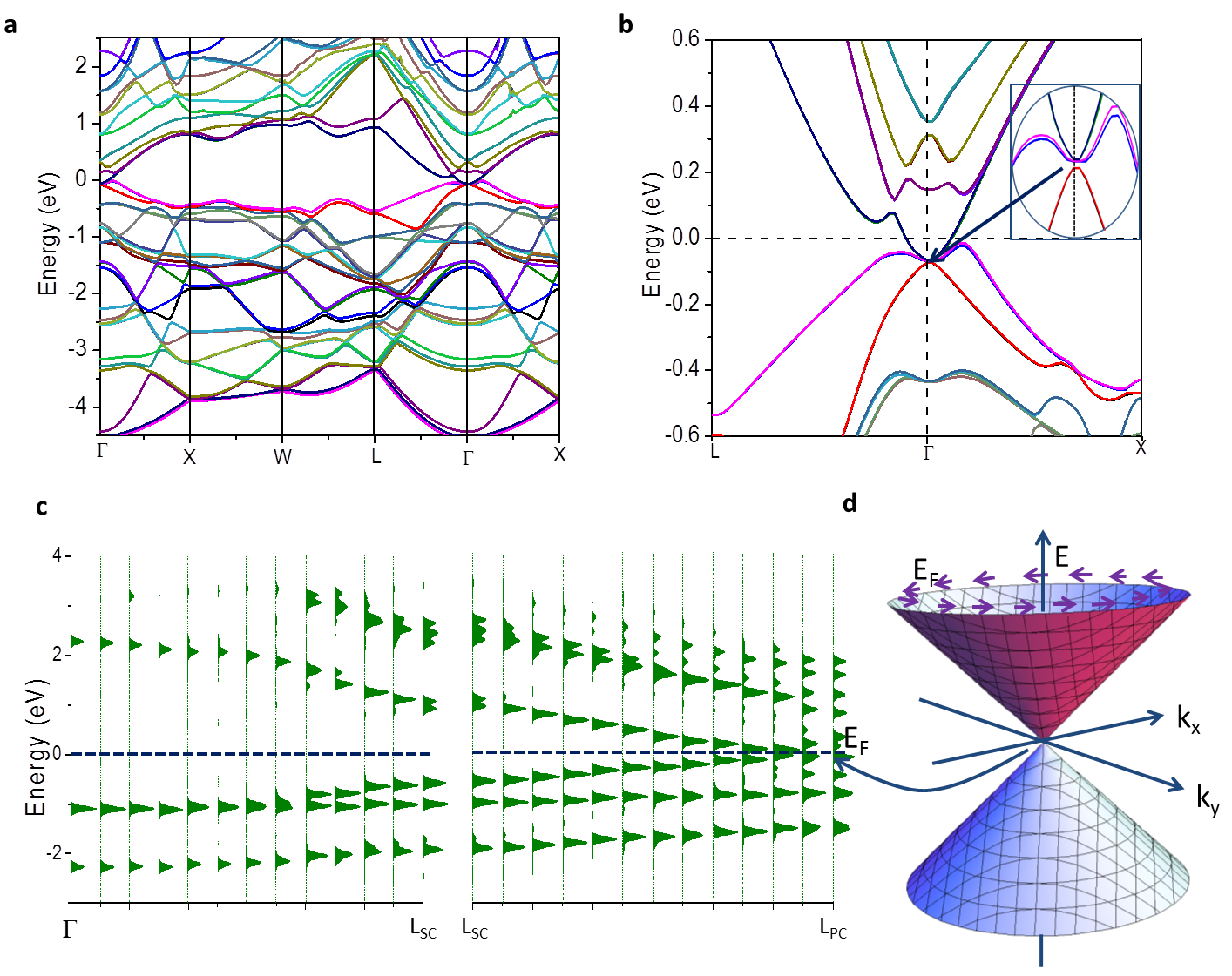
The unfolded bandstructure is equivalent to the folded bandstructure in terms of the magnitude of band separation as required by the energy conservation law. The point in the unfolded bandstructure is a mirror image of the point in the folded bandstructure, therefore, bands appear with the same dispersion as they were before unfolding. In the unfolded bandstructures, bands around the point are almost linear, which is best described by Weyl fermions. The Dirac point appears at 67 meV below the Fermi level at the point. The valence band maximum is derived from the p orbitals of Pb and Sn hybridized with the s orbital of Te and the conduction band minimum is derived from the s orbitals of Pb and Sn hybridized with the p orbital of Te. They have opposite parity, thus making interband transitions allowed. As measured in the experiment, the anisotropy in the crystal structure gives velocity components as m/s and m/s.Xu
The localization length for the Weyl states along -axis can be obtained using our calculated band gap of 350 meV including spin-orbit coupling for PbTe. Using the band velocity, m/s, we obtain nm. This length measures the characteristic scale of the confinement of Weyl states along -axis at the interface.
VI Faraday Effect for 3D TIs
In Refs. Leuenberger:2005, ; Leuenberger:2006, ; Seigneur:2011, ; Gonzalez:2010, ; Seigneur:2010, it has been shown that the single-photon Faraday rotation can be used for quantum spin memory and quantum teleportation and quantum computing with wide-bandgap semiconductor QDs. The conditional Faraday rotation can be used for optical switching of classical informationThompson:2009 . A single-photon Mach-Zehnder interferometer for quantum networks based on the single-photon Faraday effect has been proposed in Ref. Seigneur:2008, . In Ref. Berezovsky, a single spin in a wide-bandgap semiconductor QD was detected using the Faraday rotation. It is evident from the calculation above that we have strict optical selection rules for the and polarization states of the photons. We show below that these strict optical selection rules give rise to a giant Faraday effect due to Pauli exclusion principle for 3D TIs using our continuum eigenstates.
Let us consider the PbTe/Pb0.31Sn0.69Te/PbTe heterostructure shown in Fig. 8. A laser pump beam excites e-h pairs at the two interfaces between Pb0.31Sn0.69Te and PbTe. It is important to understand the working scheme of the driving fields and a dynamics of the hot carriers in the excited states so that maximum Faraday effect can be achieved in an experiment. The e-h pairs pumped by the driving field relax mainly through the electron-phonon interaction before they recombine. On a time scale of several hundred ps, the electrons and holes cool down after the driving field is turned offZhang&Wu . Due to the presence of the strong spin-orbit coupling in 3D TI, the induced spin polarization relaxes on a time scale of the momentum scattering. As calculated in Ref. Zhang&Wu , the spin polarization decays rapidly within a time of the order of 0.01–0.1 ps, which results in a loss of spin coherence. Consequently, it is very difficult to measure the Faraday effect after the pump pulse is turned off. To circumvent the problem of fast spin decoherence, we suggest to use both the pump and the probe fields simultaneously, thereby maintaining the coherence of the induced spin polarization in the excited states. Therefore, the probe field experiences a response from the spin polarized carriers. We use an off-resonant probe field with detuning energy of around 10 meV.
Let us write the light-matter interaction Hamiltonian as , which contains the interband term only because the intaband term is zero, as shown in Sec. IV. Without loss of generality, the anisotropy coming from the band velocity can be introduced back into the solutions at a later time. Since the incident light is a plane wave with wave vector and frequency and the electric field component is , the interaction Hamiltonian reads
| (34) |
where is the Kane interband matrix element. The transition rate for a single can be calculated using Fermi’s golden rule,
| (35) | |||||
where is the population distribution function for the initial and final states, is the Fermi energy, denotes the initial Weyl state, denotes the final Weyl state, and the - sign in front of corresponds to absorption and the + sign to emission. Thus, the absorption of energy per spin state is . Comparing with the total power dissipated in the system area , where is the complex conductivity, and including absorption and emission, it follows that the real part of the conductivity is
| (36) | |||||
which can be written in terms of the oscillator strengths ,
| (37) |
Using the Kramers-Kronig relations can be obtained. It is important to note that is equivalent to the imaginary part of the dieletric function, . The physical significance of and appear in different way, being for the dissipiation while for the polarization.
We calculate now the Faraday rotation angle due to Pauli exclusion principle between the initial and final continuum states. In order to this, a strong -pulse of the laser pump beam is used to excite e-h pairs. The direction of the polarization can be along and axis. The dynamics of the excitation of e-h pairs can be described by the optical Bloch equations Haug&Koch . Due to the large screening the exciton binding energies in perpendicular and parallel directions are small, i.e. eV and meV.Murphy:2006 Therefore, we can safely neglect the Coulomb interaction. Then the time dependences of the polarization and the electron population distribution for the state are given by
| (38) | |||||
| (39) |
where and are the electron and hole kinetic energies, respectively, in the state , and is the Rabi frequency. An equation similar to Eq. (39) can be written for the hole distribution function . It is to be noted that . In the rotating frame approximation, and . Using this Eqs. (38) and (39) yield and , where . These two equations can be solved for . We obtain, . A similar solution can be obtained for . For , if is an odd integer, if is an even integer, and if is an odd half-integer. A strong -pulse excites the maximum number of electrons so that with . In the absence of Coulomb interaction the Rabi frequency can be written as , where is a transitions dipole moment, is the strength of the electric field and is the direction of polarization.
It is useful to estimate the value of the Rabi frequency. The amplitude of the electric field can be calculated as , where is the power of the laser, is the index of refraction of the medium through which the light propagates and is the area of the aperture of the laser source. A laser power of 0.5 mW with an area of the aperture of in a medium with (for Pb0.68Sn0.32Te at room temperature) can produce an electric field of V/m. Using m/s and the matrix elements from Eq. (30), we obtain a maximum Rabi frequency of /s which occurs for or . During the pump beam a laser probe beam is incident on the double interface within the transparency region. The polarization of this probe beam experiences the Faraday rotation that we compute in the following.
The time dependence of the population becomes, . The pump pulse duration, , can be calculated using as . Probe and pump pulses are illuminated simultaneously to circumvent the problem of decoherence of spin polarization, as described above. Therefore, the probe pulse experiences the response from the average spin coherent population distribution excited by the pump pulse. If the probe pulse has the duration of , the average population distribution is calculated as, which gives . Since, , for and , the average of the net population distribution is . If the probe pulse has the duration of and lasts from the time to the time of the pump pulse, the average population distribution is , which gives . Thus, we obtain . These average populations give rise to the Faraday rotation of the probe field polarization.
Now we proceed to describe the Faraday effect due to the 2D Weyl fermions living at the interface of the 3D topological insulators. The difference in the phase accumulated for the and polarization of the light as it passes through the material is measured by the Faraday rotation angle, which is solely due to the difference in response of surface carriers to the and polarized light. This response of the surface carriers at the two interfaces between Pb0.31Sn0.69Te and PbTe is given by the optical conductivity tensor , , , which can be calculated by means of Eq. (37). The interband matrix element, , for the linear polarization of light in and direction can be written as
| (40) | |||||
The first and last terms of the RHS in Eq. (40) are the matrix elements that give rise to and , respectively, in and directions. The middle term gives rise to. Using Eq. (40) and the average population distribution after pumping using a linearly polarized light in direction in Eq. (37), one can solve for , and . The summation can be changed into the integration over the momentum space area, , where is the cross sectional area of the Brillouin zone. Using , k-space integration can be written as , where is the Fermi velocity. As discussed above, here we calculate the conductivity tensors for two examples of pulse duration: and . We obtain that . This signifies that there is no transverse Hall effect with this type of population distribution. If the polarization of the pump pulse is in direction the transverse conductivity is still zero. and are calculated as follows: Using the population distribution in Eq. (38), we obtain
| (41) | |||||
| (42) | |||||
Using the population distribution obtained for , Eqs. (41) and (42) yield and with and . Using the population distribution obtained for , Eqs. (41) and (42) yield and with and . These results can be compared with the conductivity tensors obtained in case of a graphene sheet in Ref. Ferreira, . The difference here is that we have use the population distribution obtained by solving the optical Bloch equations, whereas in Ref. Ferreira, the Fermi Dirac distribution function has been used.
Using Kramers-Kronig relation, can be calculated from according to
| (43) |
where denotes the Cauchy principle part of the integral. The measurement of the Faraday rotation angle is performed with the probe pulse with frequency in the transparency region. In the experiment, the probe pulse has an energy of , where is the Fermi energy and is the detuning energy. Therefore the width of the transparency region is given by . Thus, the Eq. (43) can be evaluated for . There are poles at . Using , Eq. (43) gives
| (44) | |||||
where is an infinitesimal positive quantity. Since , the first integral in Eq. (44) is zero. After evaluating the second integral we get
| (45) |
We are in the transparency region for the probe pulse, which means . The function can be then expanded in terms of a Maclaurin series at infinity, i.e. . Consequently, Eq. (45) yields
| (46) |
Similarly we obtain
| (47) |
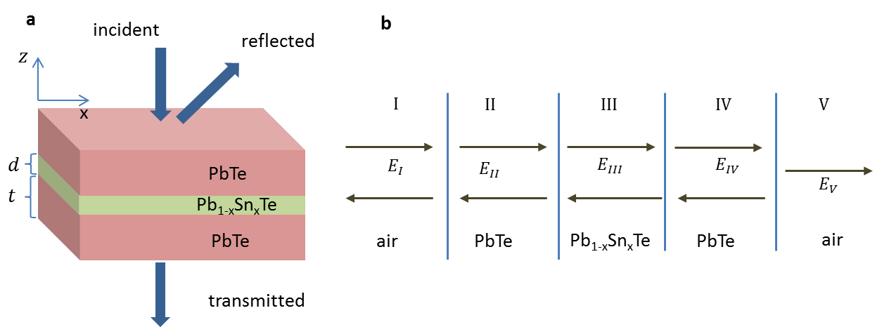
As shown in Ref. key-23-1, , there are interface bound states (IBS) localized at two decoupled interface states of a PbTe/Pb1-xSnxTe/PbTe heterostructure with nm grown in the [111] direction. It has been shown that the L-valley in [111] direction remains gapless while gaps are opened in the oblique L valleys due to the coupling of the IBS from the opposite interface states. Here we calculate the Faraday rotation angle produced by the Weyl fermions at the two interfaces with gapless L valley. We consider a structure with a slab of thickness of 3D TI material Pb1-xSnxTe sandwiched by PbTe with thickness , as shown in Fig. 8a. We choose the thickness of the slab to be nm. A probe pulse linearly polarized along the -direction and propagating along -direction travels perpendicularly to the two interfaces. This probe pulse is partially reflected and partially transmitted at the boundaries. Solutions inside and outside the material can be solved by dividing the space into five different regions as shown in Fig. 8b, where , , , and ,are the fields in the region , , , and , respectively. The solutions are
| (52) | |||||
| (57) | |||||
| (62) | |||||
| (67) | |||||
| (70) |
where (), , are the () components of the field amplitudes in regions through . , and are the wave vectors in air (region ), in PbTe (region ) and in Pb1-xSnxTe (region ), respectively. The incident probe pulse is polarized along the -axis. Therefore . For simplicity, we assume that the wave vectors within the material Pb1-xSnxTe and PbTe do not differ significantly and thus .
Our geometry has a dimension of length with top, bottom, and interface surfaces being parallel to the plane of polarization. Rotation of the polarization on the Poincare sphere is due to the charge carriers at the interfaces, which are excited by the pump pulse with energy at least twice the Dirac point energy measured from the Fermi level (see Fig. 3). The accumulation of the phase difference is only due to surface carriers that come from the difference in the optical conductivity tensor for the and polarization of the light. There is no contribution to the phase shift in the polarization from the bulk. However, the index of refraction of the bulk leads to interference effects due to reflection and transmission at the boundaries. The Maxwell equations to be solved are given byFerreira
| (71) | |||||
where is the permeability of the free space and is the dielectric constant of the material in the bulk. It is important to note that the delta functions ensure that the optical conductivity tensor originates only from the interface carriers. The optical conductivity tensor that enters Maxwell’s equations is the imaginary part of , i.e. [see Eqs. (46) and (47)], which gives rise to the dispersion of the incident light inside the material. The boundary conditions are determined by the continuity of the tangential components of the electric field and their derivatives at the boundaries of the materials at , , and . The details of matching of the fields at the boundaries are shown in Appendix A. The transmission amplitudes for and components of the electric field are calculated to be , where is the transmission amplitude and are the Faraday rotation angles for the light polarized in and direction. and are given by
| (72) | |||||
| (73) | |||||
where () , (), () and () are the () components of the parameters , , and , respectively (see Appendix A). After solving Eqs. 72 and 73 for and , we write the Faraday rotation angle as . The useful quantity, the total transmittance, which measures the energy of the electromagnetic field inside the material, can be defined as .
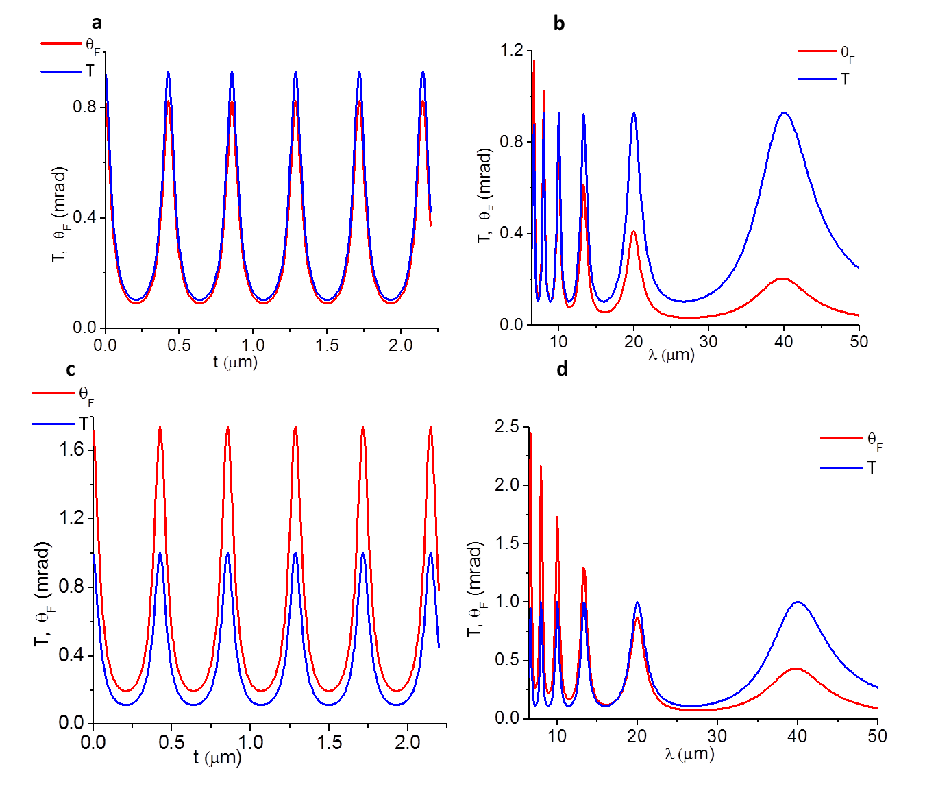
From the bandstructure calculation we obtain that the Fermi level lies around 67 meV below the Dirac point. Therefore, we choose a transparency energy gap of , which is 134 meV in our calculation. A linearly polarized probe pulse with detuning energy of meV, pulse duration of 1 ps and bandwidth of meV can be used. In Figs. 10 a and b we show the transmittance and the Faraday rotation angle for . In Figs. 10 c and d the transmittance and the Faraday rotation for are shown. For the transmittance and the Faraday rotation angle as a function of thickness the wavelength is chosen to be . For the transmittance and the Faraday rotation angle as a function of wavelength the thickness of PbTe layers is taken to be . It is seen from the figures that the Faraday rotation angle follows exactly the transmittance. In particular, the maxima of the Faraday rotation angle occur at the maxima of the transmittance, which corresponds the case of nearly reflectionless slab in optics. There are two cases when reflection turns to zero. The first case is given by the half-wave condition when , is an integer and . The second case is given by the quarter-wave condition when , , where is the total length of the slab, is an integer, , and are the indices of refraction of a slab of material and of the materials on either side of the slab, respectively. In our case the half-wave condition is met. Therefore, the resonances are seen (Fig. 10b) inside the material at half-integer multiples of the probe wavelength divided by the index of refraction of the material, which is . Of course, Fig. 10 exhibits a slight deviation from zero reflection at maxima due to the presence of multiple interfaces. The Faraday rotation angle obtained using a wide-bandgap semiconductor quantum dot is usually small compared to this result. Berezovsky
VII Conclusion
We have calculated the optical transitions for the Weyl interface fermions in 3D TI at the point using the Dirac Hamiltonian. The spin selection rules for the optical transitions are very strict. The interaction Hamiltonian that comes from the quadratic part of the k. p is included in the calculation and is shown to have zero contribution to the transition dipole moment.
We demonstrate the effect of the strict optical selection rules by considering the Faraday effect due to Pauli exclusion principle in a pump-probe setup. Our calculations show that the Faraday rotation angle exhibits oscillations as a function of probe wavelength and thickness of the slab material on either side of the 3D TI double interface of a PbTe/Pb0.31Sn0.69Te/PbTe heterostructure. The maxima in the Faraday rotation angle are in the millirad regime.
Acknowledgements.
We acknowledge support from NSF (Grant ECCS-0901784), AFOSR (Grant FA9550-09-1-0450), and NSF (Grant ECCS-1128597). We thank Gerson Ferreira for useful discussions. M.N.L. thanks Daniel Loss for fruitful discussions during his stay at the University of Basel, Switzerland. M.N.L. acknowledges partial support from the Swiss National Science Foundation.Appendix A
The continuity of the tangential components of the electric field at , , and leads to
| (82) | |||||
| (92) | |||||
| (102) | |||||
| (110) | |||||
Similarly the continuity of derivative of the electric fields at , , and yields
| (119) | |||||
| (131) | |||||
| (143) | |||||
| (150) | |||||
The response of the top and bottom surfaces of the Pb1-xSnxTe slab to the field depends on the transition matrix elements on the corresponding surfaces. Since, the transition matrix elemets for both of the surfaces are same, we have . The off diagonal elements and of the magneto-optical tensors are calculated to be zero. The algebric Eqs. 82 to 150 can be solved for each of the amplitude of component field in each region interm of the incident filed. The solutions for the transmitted field are given by
| (151) |
where , ,
| (154) | |||||
| (157) | |||||
| (166) | |||||
| (175) |
References
- (1) Moore, J. E. The birth of topological insulators. Nature 464, 194 (2010).
- (2) M. Z. Hasan, C. L. Kane, Rev. Mod. Phys. 82, 3045 (2010).
- (3) D. Hsieh, Y. Xia, D. Qian, L. Wray, J. H. Dil, F. Meier, J. Osterwalder, L. Patthey, J. G. Checkelsky, N. P. Ong, A. V. Fedorov, H. Lin, A. Bansil, D. Grauer, Y. S. Hor, R. J. Cava, M. Z. Hasan, Nature 460, 1101-1106 (2009).
- (4) M. Hajlaoui, E. Papalazarou, J. Mauchain, G. Lantz, N. Moisan, D. Boschetto, Z. Jiang, I. Miotkowski, Y. P. Chen, A. Taleb-Ibrahimi, L. Perfetti, M. Marsi, Nano Lett. 12, 3532-3536 (2012).
- (5) Y. Xia, D. Qian, D. Hsieh, L. Wray, A. Pal, H. Lin, A. Bansil, D. Grauer, Y. S. Hor, R. J. Cava, M. Z. Hasan, Nature Physics 5, 398 (2009).
- (6) D. Hsieh, D. Qian, L. Wray, Y. Xia, Y. S. Hor, R. J. Cava, M. Z. Hasan, Nature 452, 970-974 (2008).
- (7) I. Knez, R. R. Du, G. Sullivan, Phys. Rev. Lett. 107, 136603 (2011).
- (8) H. Zhang, C.-X. Liu, X.-L. Qi, X. Dai, Z. Fang, S.-C. Zhang, Nature Physics 5, 438 (2009).
- (9) Y. A. Bychkov, E.I. Rashba, JETP Lett. 39, 78 (1984).
- (10) C. L. Kane, E. J. Mele, Phys. Rev. Lett. 95, 146802 (2005).
- (11) L. Fu, C. L. Kane, Phys. Rev. B 76, 045302 (2007).
- (12) J. E. Moore, L. Balents, Phys. Rev. B 75, 121306(R) (2007).
- (13) L. Fu, C. L. Kane, E. J. Mele, Phys. Rev. Lett. 98, 106803 (2007).
- (14) Y. L. Chen, J. G. Analytis, J.-H. Chu, Z. K. Liu, S.-K. Mo, X. L. Qi, H. J. Zhang, D. H. Lu, X. Dai, Z. Fang, S. C. Zhang, I. R. Fisher, Z. Hussain, Z.-X. Shen, Science 325, 178 (2009).
- (15) J. O. Dimmock, I. Melngailis, A. J. Strauss, Phys. Rev. Lett. 16, 1193 (1966).
- (16) O. A. Pankratov, Semicond. Sci. Technol. 5, S204-S209 (1990).
- (17) V. Korenman, H. D. Drew, Phys. Rev. B 35, 6446 (1987).
- (18) D. Agassi, V. Korenman, Phys. Rev. B 37, 10095 (1988).
- (19) B. A. Volkov, O. A. Pankratov, JETP Lett. 42, 178 (1985).
- (20) X. Gao, M. S. Daw, Phys. Rev. B 77, 033103 (2008).
- (21) Su-Y. Xu, C. Liu, N. Alidoust, M. Neupane, D. Qian, I. Belopolski, J. D. Denlinger, Y. J. Wang, H. Lin, L. A. Wray, G. Landolt, B. Slomski, J. H. Dil, A. Marcinkova, E. Morosan, Q. Gibson, R. Sankar, F. C. Chou, R. J. Cava, A. Bansil, and M. Z. Hasan, Preprint arxiv.1210.2917.
- (22) V. Popescu, A. Zunger, Phys. Rev. B 85, 085201 (2012).
- (23) W. Ku, T. Berlijn, C. C. Lee, Phys. Rev. Lett. 104, 216401 (2010).
- (24) M. N. Leuenberger, M. E. Flatté, D. D. Awschalom, Phys. Rev. Lett. 94, 107401 (2005).
- (25) M. N. Leuenberger, Phys. Rev. B 73, 075312 (2006).
- (26) H. P. Paudel, M. N. Leuenberger, to be published in Phys. Rev. B; see preprint arXiv:1212.6772.
- (27) W.-K. Tse and A. H. MacDonald, Phys. Rev. Lett. 105, 057401 (2010).
- (28) G. Nimtz and B. Schlicht, in Narrow Gap Semiconductors (Springer, Berlin, 1983), pp. 45-48.
- (29) R. Buczko, L. Cywinski, Phys. Rev. B 85, 205319 (2012).
- (30) A. de Silva, G. C. La Rocca, F. Bassani, Phys. Rev. B 55, 16293 (1997).
- (31) Y. Zhao, Y. Hu, L. Liu, Y. Zhu, H. Guo, Nano Lett. 11, 2088-2091 (2011).
- (32) H. Yusheng, A.D.C. Grassie, J. Phys. F: Met. Phys. 15, 363-376 (1985)
- (33) J. J. Sakurai, Advanced Quantum Mechanics (Addison-Wesley, New York, 1994).
- (34) P. Y. Yu, M. Cardona, Fundamentals of Semiconductors: Physics and Materials Properties (Springer, Berlin, 3rd edition, 2005).
- (35) G. Kresse, J. Furthmuller, Phys. Rev. B 54, 11169 (1996).
- (36) G. Kresse, J. Hafner, J. Phys.: Condens. Matter 6, 8245 (1994).
- (37) P.E. Blochl, Phys. Rev. B 50, 17953 (1994).
- (38) Su-Y. Xu, C. Liu, N. Alidoust, M. Neupane, D. Qian, I. Belopolski, J. D. Denlinger, Y. J. Wang, H. Lin, L. A. Wray, G. Landolt, B. Slomski, J. H. Dil, A. Marcinkova, E. Morosan, Q. Gibson, R. Sankar, F. C. Chou, R. J. Cava, A. Bansil, and M. Z. Hasan, Nature Comm. 3, 1192 (2012).
- (39) H. P. Seigneur, G. González, M. N. Leuenberger, W. V. Schoenfeld, Adv. OptoElectron. 2011, 893086 (2011).
- (40) G. González, H. P. Seigneur, W. V. Schoenfeld, Michael N. Leuenberger, J. Comput. Theor. Nanosci. 7, 1651 (2010).
- (41) H. P. Seigneur, G. González, M. N. Leuenberger, W. V. Schoenfeld, Adv. Math. Phys. 2010, 342915 (2010).
- (42) A. V. Thompson, H. P. Seigneur, M. N. Leuenberger, W. V. Schoenfeld, IEEE J. of Quantum Electronics 45, 637 (2009).
- (43) H. P. Seigneur, M. N. Leuenberger, W. V. Schoenfeld, J. Appl. Phys. 104, 014307 (2008).
- (44) H. P. Seigneur, M. N. Leuenberger, W. V. Schoenfeld, J. Appl. Phys. 104, 014307 (2008).
- (45) J. Z. Salvail, M. Agnew, A. S. Johnson, E. Bolduc , J. Leach, R. W. Boyd, Nature Photonics, 7, 316, (2013).
- (46) H. Haug, S. W. Koch, Quantum Theory of The Optical and Electronic Properties of Semiconductors (World Scientific Publishing, Singapore, 2001).
- (47) J. E. Murphy, M. C. Beard, A. G. Norman, S. P. Ahrenkiel, J. C. Johnson, P. Yu, O. I. Micic, R. J. Ellingson, A. J. Nozik, J. Am. Phys. Soc. 128, 3241 (2006).
- (48) A. Ferreira, J. Viana-Gomes, Yu. V. Bludov, V. M. Pereira, N. M. R. Peres, A. H. Castro Neto, Phys. Rev. B 84, 235410 (2011).
- (49) K. F. Mak, M. Y. Sfeir, Y. Wu, C. H. Lui, J. A. Misewich, and T. F. Heinz, Phys. Rev. Lett. 101, 196405 (2008).
- (50) J. P. Reithmaier, G. Sek, A. Loffier, C. Hofmann, S. Kuhn, S. Reitzenstein, L. V. Keldysh, V. D. Kulakovskii, T. L. Reinecke, A. Forchel, Nature 432, 197 (2004).
- (51) J. Berezovsky, M. H. Mikkelsen, O. Gywat, N. G. Stoltz, L. A. Coldren, D. D. Awschalom, Science 314, 1916 (2006).
- (52) Jonghwan Kim, Hyungmok Son, David J. Cho, Baisong Geng, Will Regan, Sufei Shi, Kwanpyo Kim, Alex Zettl, Yuen-Ron Shen, and Feng Wang, Nano Lett. 12, 4498-5602 (2002).
- (53) P. Zhang and M. W. Wu, Phys. Rev. B 87, 085319 (2013).