Electron irradiation induced reduction of the permittivity in chalcogenide glass (As2S3) thin film
Abstract
In this paper we investigate the effect of electron beam irradiation on the dielectric properties of As2S3 Chalcogenide glass. By means of low-loss Electron Energy Loss Spectroscopy, we derive the permittivity function, its dispersive relation, and calculate the refractive index and absorption coefficients under the constant permeability approximation. The measured and calculated results show a heretofore unseen phenomenon: a reduction in the permittivity of . Consequently a reduction of the refractive index of , hence suggesting a conspicuous change in the optical properties of the material under irradiation with a electron beam. The plausible physical phenomena leading to these observations are discussed in terms of the homopolar and heteropolar bond dynamics under high energy absorption. The reported phenomena, exhibited by As2S3-thin film, can be crucial for the development of photonics integrated circuits using electron beam irradiation method. Published at Journal of Applied Physics 113, 044116, 2013. DOI: 10.1063/1.4789602
pacs:
77.84.Bw, 79.20.Uv, 77.22.Ch, 61.80.FeI Introduction
Over the last decades, chalcogenide glasses have been a subject of great interest due to the myriad photon-induced phenomena they exhibit, captivating the imagination of scientists and engineers to prompt countless photonic applications ranging from biologyYang2010 ; Eggleton2011 and telecommunicationsPelusi2010a ; Eggleton2010 , all-optical chipsEggleton2010 ; Eggleton2011 , single photon sourcesXiong2010 ; Bendana2011 to holographyJuodkazis2004 . Furthermore, they have been worthy of great attention from fundamental science, owing to the seemingly oxymoronic nature of the physical effects observed when the material is illuminated by photons within its band-gap energy range () , e.g. giant photo-expansionChen1970 versus photo-contractionKozak2009a , photo-liquidityFritzsche1996a ; Tanaka2005 versus photo-crystallizationFeinleib1971 ; Tanaka2009 , photo-darkeningIstvan2007 ; DeNeufville1974 versus photo-bleachingIstvan2007 , and, more frequently, photo-refractionDeNeufville1974 ; Gopal1982 ; Kurtz2009 ; VKTikhomirovandSRElliott1995 , to cite a few. Studies from fundamental physics and material science have led to various models attempting to explain the mechanisms behind the exciting structural reconfiguration capabilities and phenomena observed in chalcogenide glasses upon energy absorption. That being said, the physical processes, in addition to many of the phenomena reported, remain both a matter of debate and a hot topic in fundamental and applied research.
The principal experiments, observations and models in chalcogenide glass deal with phenomena triggered by light irradiation. Photon induced phenomena in chalcogenide glass comprises: photon-induced -refractive index modification, -liquidity, -dichroism, -anisotropy, -crystallization, -darkening, -bleaching, and -vitrification Chen1970 ; Kozak2009a ; Fritzsche1996a ; Tanaka2005 ; Feinleib1971 ; Tanaka2009 ; Istvan2007 ; DeNeufville1974 ; Gopal1982 ; Kurtz2009 ; VKTikhomirovandSRElliott1995 ; Submitted2010 , in addition to other innate effects present in highly non-linear materials, v.gr. second harmonic generation Ta'eed2006 ; Lyubin2006 for example. To understand the nature of these effects, and the electronic and atomic processes involved, it is essential to investigate the charge carrier transfer, energy spectrum, and the mechanisms by which radiation (electron or photon) interacts with the material modifying its chemical and atomic structure Kozak2009a ; Tanaka2005 ; Tanaka2009 ; Anderson1975 ; Fritzsche1998 ; Simdyankin2004 ; Andriesh2004 ; Singh2007 .
Electron irradiation induced refractive index modification has also previously been observed. Suhara et al.Suhara1975 , found a maximum change of , with no significant modification in the thickness of the film. On the other hand, Normand et al.Nordman1996a ; Nordman2001a ; Nordman2001 and Tanaka et al.Tanaka1997a , independently observed a increment in the refractive index of chalcogenide glass; simultaneously the formation of trenches and mounds, and respectively, in chalcogenide films of thick, were observed. They posited that the morphological and optical alteration derives from the structural reorganization and re-bonding of the homopolar and heteropolar bonds, in addition to the electrostatic effects arising from the charge density variation Nordman1996a ; Nordman2001a ; Nordman2001 ; Tanaka1997a .
Whilst many of these effects appeal to our research interest, we are particularly intrigued by the alteration in the optical properties of chalcogenide glass thin films, and its possible applications. However, in most of the previous studies only the refractive index has been characterized, with little information available on how the electromagnetic components, i.e. permittivity and permeability, reshape under energy absorption. In this paper we present the results of our investigation on the permittivity dynamics of chalcogenide glass As2S3 thin film under energy absorption by means of low-loss electron energy loss spectroscopy (EELS). We believe that understanding the electromagnetic characteristics, and their dynamics, particular to this material are key to enabling and extending many of the devices proposed by transformation optics and achieving light control beyond the scope of [meta]materials.
To this effect, we have organized the paper as follows; Section I presented a review; section II introduces the theoretical and experimental methodology needed to explain the experimental results; section III presents the results and analysis, followed by the deduction of the refractive index under the constant permeability approximation, while discussing its implications; finally, section IV, we present our conclusions.
II Methods
It is worth to discern the difference, and connection, between the refractive index and the electromagnetic properties of materials. The former is the ratio between the propagation speed of waves inside a material to that of vacuum; whereas the latter, permittivity () and permeability (), are the physical representation of a material’s intrinsic electric and magnetic properties; which arise from the atomic, electronic and molecular configuration and interactions with the electric and magnetic fields, ultimately shaping their propagation dynamics. Accordingly, the refractive index and the electromagnetic properties of materials are entwined by the widespread relation: , where the subscript refers to the relative permittivity or permeability, i.e. and .
Permeability and permittivity are, then, key to manipulate light propagation in materials, and hence the importance of characterizing them, and understanding how can they be modified.
II.1 Electron Energy Loss Spectroscopy
As discussed earlier, As2S3 chalcogenide glass, exhibits electron- and photon- irradiation induced modification of its optical properties. In our study we use low-loss EELSPerrin1974 ; Egerton1996 to characterize the real and imaginary parts of the permittivity of As2S3.
When high energy electrons, keV impinge on a sufficiently thin material, thickness , a vast majority of the electrons will pass through the sample without being perturbed, and a small fraction of them will undergo inelastic scattering loosing energy to the sample, typically in the order of . It is important to note, however, that some of the electrons will also be elastically scattered and will transfer some energy to the system; yet, this energy is not enough to perturb the overall atomic arrangement of the material, even on a head-on collision with the atom the elastic scattered electron energy loss will be in the range of , which is not sufficient to displace the atoms and therefore change the molecular arrangement. The inelastic scattering, nevertheless, yields enough energy to the system to sustain bond-breaking and alterations in the electron density of the material. The latter electron loss can be experimentally measured via an electron spectrometer.
The inelastic scattering process is characterized by the electron scattering angle, , or momenta, , and the electron energy loss, , due to their interactions with the material, which includes phonon excitation, inter- and intra- band transition, plasmons excitation, inner shell ionization, and Cherenkov radiation. These interactions can be summarized by the dielectric response function, ; which describes the interaction of photons and electrons with the material Egerton1996 .
Admittedly, the interaction of photons and electrons with those in the solid is different; photons displace the electrons in the material in a direction perpendicular to their direction of propagation, with the electron density remaining unchanged. Therefore, we define the optical permittivity as a transverse property of a medium; whereas electrons interacting with the material produce a longitudinal displacement of the electrons, and change the electron density. Moreover, the energy transfer mechanisms for photons differs from that of electrons; in the former the energy transfer is mostly mediated by inter- and intra- band transitions (valence-to-conduction band), e.g. (i) bandgap absorption, (ii) defects, (iii) free carriers, among other transitions. In the scenario of electron irradiation, energy transfer takes place by means of inelastic scattering, and to a lesser degree by elastic scattering. Despite the fundamental differences, however, it is possible to establish a correlation between the permittivity measured by electrons or photons if we constrain to small energy losses, which translates small scattering angles for electrons. Under this condition varies insignificantly with , and hence , the latter being the optical permittivity Egerton1996 ; Ritchie1957 ; Nozieres1959 .
Whence stems the versatility of low-loss EELS over other methods to measure the permittivity of thin film samples constraint to small probing areas. Specifically, if scanning transmission microscopy (STEM) is used, the volume of study can be reduced to nano-metric scale, allowing us to study the material and its response locally. As discussed in the preceding paragraph in a typical EELS experiment low angles of collections are used, and thus most inelastic collisions result in energy losses to the incoming electrons of less than . This energy loss range in turn deciphers information about the permittivity within an energy range of interest to optics and photonics, i.e. . The latter is achieved by post-processing the energy loss spectra by means of Kramers-Kronig relations to evince the real and imaginary parts of the optical permittivity Egerton1996 ; Stoger-Pollach2008 ; Egerton2009 ; Verbeeck2009 ; GarciadeAbajo2010 ; Zhang2010b ; Schafer2012 .
II.2 Experimental arrangement
In our experiment, high energy electrons () impinge on an As2S3 thin film, thick, grown on a holey-Cu TEM grid by means of electron-beam evaporation, and the roughness, film thickness and stoichiometry are characterized by atomic force microscopy (AFM), ellipsometry, energy dispersive X-ray (EDX), and X-ray photoemission spectroscopy (XPS), respectively.
To ensure the validity of the low energy loss limit approximation, we use a scanning transmission electron microscope (STEM), coupled to a low-loss EELS, and perform the experiment in the low momentum transfer relativistic approximation. We set the electron source to , with a collection angle of , and incident semi-angle of . Under these conditions the energy resolving power of the electron loss spectrometer is better than in the range ; electrons are accelerated to the speed of light, corresponding to a de Broglie wavelength of , which results in a minimum spatial resolution of . The scanning area for the STEM is on the holey region of the film support to avoid any contamination from the carbon support of the grid. The density of electrons per second incident on the sample is 175 . To achieve different electron dosages we control the irradiation time in steps of (see table 1). These steps are divided into two irradiation sequences, sequence and sequence ; which are separated by a relaxation time defined as the period of time where zero electrons are incident on the film. This arrangement allows us to determine if after a given time of repose the material returns to its initial state, i.e. if it exhibits memory or a hysteretic behaviour.
| Sequence A | Relaxation | Sequence B | |||||
|---|---|---|---|---|---|---|---|
| Irradiation steps (step) | 1 | 2 | 3 | 4 | pause | 5 | 6 |
| Irradiation exposure time | 0.1 | 0.2 | 0.3 | 0.5 | 60 | 0.8 | 1.0 |
| Accumulated irradiation time | 0.1 | 0.3 | 0.6 | 1.1 | - | 0.8 + 1.1 | 1.8 + 1.1 |
III Observations and analysis
As discussed earlier in the text, we study the energy loss spectra of transmitted electrons in the low momentum transfer relativistic approximation, customarily known as low-loss EELS. The experiment results is a spectra-like graph detailing the density of electrons versus their output energy at different irradiation dosages.
III.1 Results analysis
In order to obtain the optical and electronic characteristics of the material, the loss spectra needs to be deconvoluted, and the zero loss subtracted: this is attained by the Fourier-Log Two Gaussian method Egerton1996 (see figure 1).
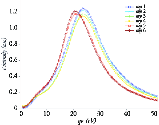
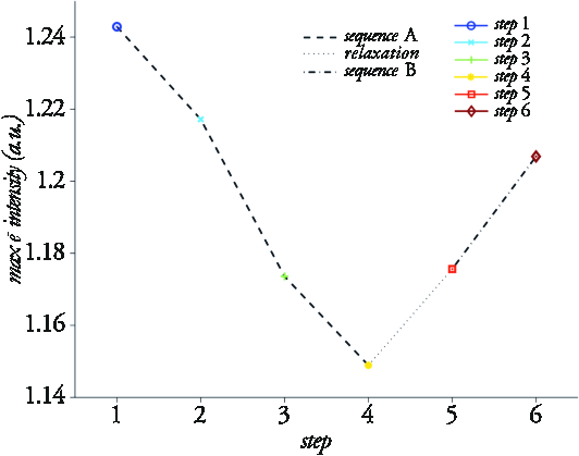
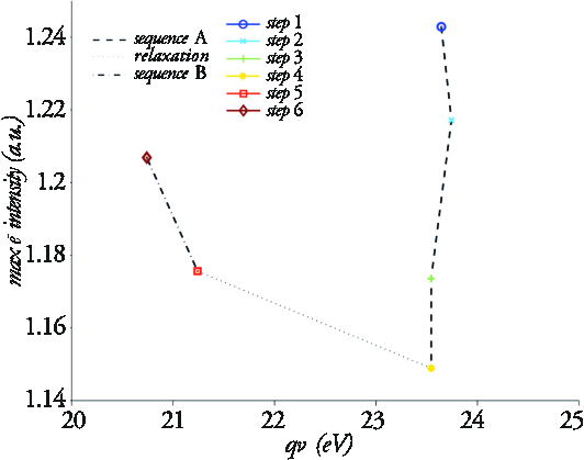
A meticulous inspection of figure 1 reveals that the peak of the loss spectra decreases as a function of electron dosage, as depicted in figure 2a, after irradiation sequence A, and before relaxation, the peak value changes . It is also evident that the process has some degree of elasticity, where after relaxation some recovery occurs such that the electron intensity before and after relaxation suffers a return (see figure 2a). However, this return goes hand in hand with a blue-shift of the peak dispersion of (see figure 2b). Yet there is a striking effect, subsequent irradiation for long periods of time has a reverse effect, increasing the total electron intensity rather than decreasing it as was the case before relaxation in sequence A. As we will elucidate later this effect can be explained by the breaking of the homopolar bonds, and the continuous reconfiguration of the heteropolar bonds within the material. It is capital to recall that our experiment is carried in a vacuum environment (), therefore eliminating any chance of oxidation and contamination on the material surface.
As discussed earlier, the electron energy loss is linked to the real and imaginary permittivity (see equation 1), and hence we can expect them to follow a somewhat similar pattern to that of the energy loss. Egerton1996 .
| (1) |
By virtue of the above equation and the Kramers-Kronig relations we obtain the imaginary part of the permittivity function, , and the real part, , here shown in figure 3.
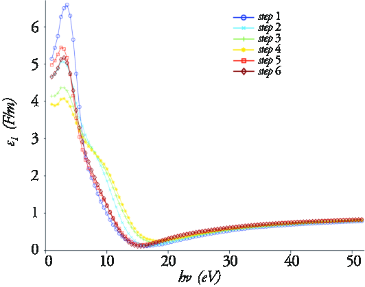
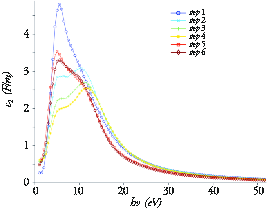
It is essential for the ongoing discussion to remark that in the curves of figure 3, and subsequent, the causal variable, , refers to the photon energy, for recall that these result from the Kramer-Kronig analysis of the electron energy loss spectra at the low momentum approximation. Therefore, they can be regarded as dispersion relations for the permittivity at different electron irradiation dosages.
As predicted at analyzing the electron energy loss spectra, the real and imaginary parts of the permittivity decrease as the electron dosage augments. Moreover, figures 3c and 3d confirm the semi hysteretic comportment of the permittivity. Particularly, observe that the maxima of reduces, and shifts following a semi hysteresis loop, as the total dosage rises; while its minima shifts to higher energies, although seldom changing its dispersion energy . On the other hand, the maxima of exhibits a similar decrement, as that portrayed by as a function of dosage, with the difference that there is no evidence of a hysteretic behaviour, rather the maximum shifts to higher energies together with electron dosage.
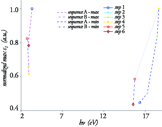
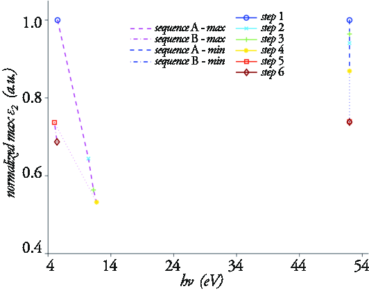
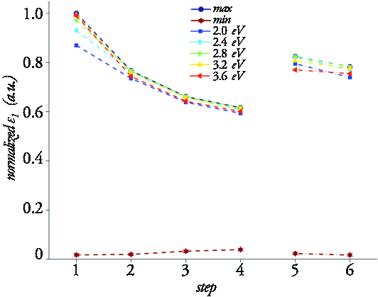
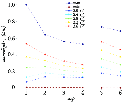
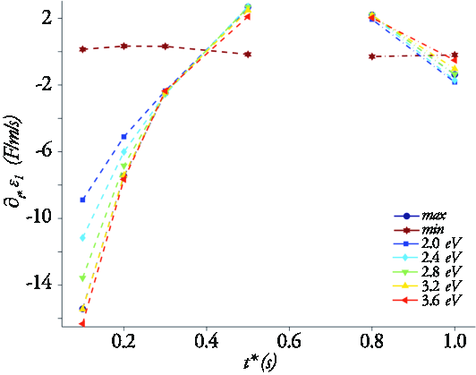
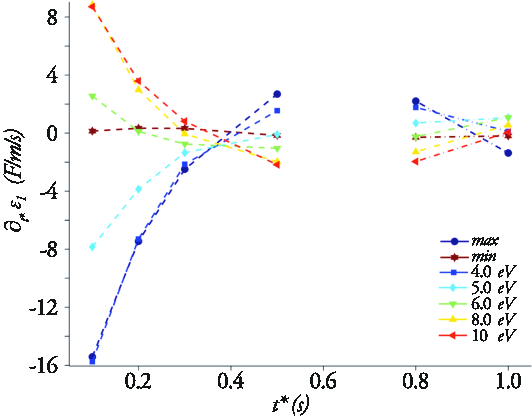
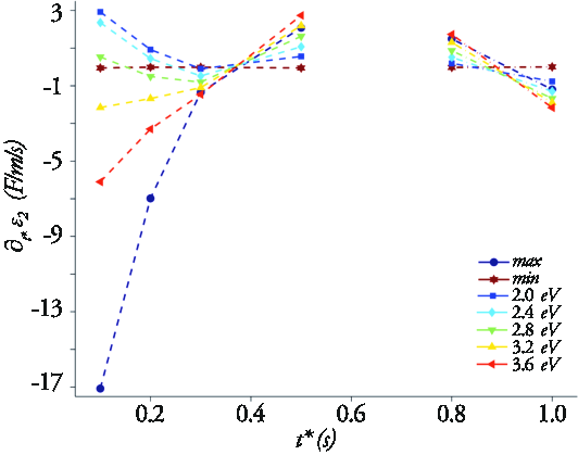
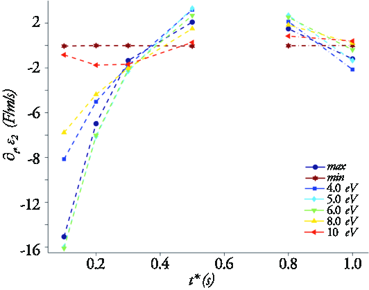
To acquire a deeper insight on the permittivity of the material and its dynamics we sampled it by splitting the dispersion energy range in two, range A comprises energy values around the bandgap of the material, i.e. ; and range B includes higher energies . At either set we compare the results to the global maximum and minimum, denoted by max and min, receptively. Within range A the sampling results, figures 4a and 4c, clearly evince the hysteretic behaviour of the electron-induced permittivity change. At comparing the curves given by the maximum peaks of and , before and after relaxation, it is patent that some degree of restoration occurs in the system which allows a recovery of up to of the initial values. Furthermore, the dynamics of the extreme values of either the real or imaginary permittivity echo an almost identical pattern, with an initial fast rate of change during the first irradiation steps , closely followed by a sustained decrement on its absolute value, i.e. the pace at which the permittivity changes tends to zero for a sufficiently large irradiation time (see figures 5). As we will explain in section III.2 this effect can be understood through the variation in the density and rearrangement of the homopolar and heteropolar bonds, which significantly modifies the response of the material to energy absorption.
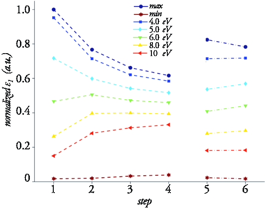
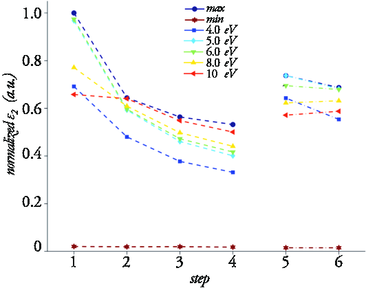
As it can be appreciated at comparing the results between the two energy ranges, either for real or imaginary parts of the permittivity, shows significantly different comportments. The test values for the real permittivity in range A closely follow the pattern and magnitude modification of the global maximum, while the global minimum remains virtually unperturbed. In range B, however, the selected values present different bearing to that observed previously. Specifically, before relaxation, samples at initially increase in magnitude as much as , in contrast to the marked decrease of the global maximum. Yet, with the exception of the sample at subsequent electron exposures regain the decreasing pattern of the maximum, albeit to a lesser magnitude, and rate of change (see figure 5b). After relaxation, however, some degree of elasticity is observed, with most of the test samples recovering to the initial state, although exposing the relaxed material anew to electron irradiation results in an increment of the permittivity value in clear contrast to the global maximum bearing.
Concerning the imaginary part of the permittivity, the previous description gets somewhat inverted when compared to the measurements of in both ranges. In range A the initial behaviour is mixed, with some of the samples increasing in magnitude, while others decrease. Notably, test samples below the band-gap energy of the material show a similar behaviour to that of the imaginary permittivity in range A, an initial increment followed by a steady decrease with new dosages. Range B on the other hand shows a behaviour close to the comportment of the global maximum, with the anomaly of test sample at . After relaxation the degree of recovery is mixed, in range B the hysteretic behaviour is conspicuous. But in range A the results are to some extent extraordinary, all the samples beyond the band-gap of the material show some degree of recovery, in some cases surpassing the initial value by as much as for example at ; below the band-gap energy test samples show an eerie result not only there is no recovery to the initial state, but a considerable increment instead. After relaxation all samples show the same decreasing pattern as observed in their real counterpart. In range B all the samples follow a similar pattern to that of the maximum; an initial fast decrease, followed by a sustained decrease in magnitude, although steadily reducing the rate of change. The physical explanation to this peculiar reaction of the material, reflected by the permittivity, in response to electron bombardment can be reasoned in term of the modification to the physical bonding between the Arsenic and Sulfide atoms, and the electron traps within the material, assuming that there is no increment in the initial number of electrons in the material, which to this effect is grounded.
III.2 Physical process
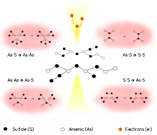
To fathom the physical process behind this phenomenon it is necessary to gain some understanding about the atomic configuration of As2S3 chalcogenide glass. Either amorphous or crystalline, the structure of chalcogenide material based on As and S is composed of pyramidal arrangement in threads that form layers linked by homopolar (As–As and S–S) and heteropolar (As–S) bonds (figure 6). The bonding energies in the homopolar case are and for As–As and S–S bonds, respectively; whilst for the heteropolar (As–S) the bonding energy is Ramirez-Malo1994 . Our film has similar proportions of As and S atoms, and respectively, as measured by XPS in the surface of the material. To evaluate the overall bulk composition of the film we use EDX finding atomic proportions closer to that of As2S3 chalcogenide glass (As and S ). The atomic composition measured before and after the experiment by EDX did not show any net flux of atom concentration. It is important to note that our TEM instrument has the ability to do STEM, TEM and EDX within the same chamber, thus avoiding the possibility of contamination or oxidation of the sample by keeping it under high vacuum. Under irradiation exposure the incoming electrons () can break the homopolar and heteropolar bonds with ease by mean of inelastic collisions; whence a structural rearrangement follows, with the broken homopolar bonds switching to heteropolar bonds Nordman1998 ; Kovalskiy2008 . This structural rearrangement will continue for as long as the material keeps being bombarded with electrons. However, since the concentration of As atoms is higher, the re-bonding of the S and As atoms, mostly coming from the broken homopolar bonds, will lead to dangling uncoordinated As atoms. Under relaxation, the dangling As atoms, in vacuum, re-bond in homopolar As–As pairs. Consequently, the density of homopolar bonded As increases, resulting in a diminished response to electron irradiation as observed in the decrement in the rates of change before and after the first irradiation and relaxation period 5.
Concomitant to the re-bonding process is the nano-crystallization of the material, which causes a reduction in the number of the trapped carriers, either by promoting a large fraction of the electrons to the conduction band, or by reducing the number of carrier traps in the material. The overall modification of the electronic density states originates the prominent reduction in the permittivity. Recall that in amorphous and semi-crystalline materials the permittivity heavily depends on the density of trapped carriers. This comes from the fact that carrier transport in these materials, like chalcogenide glass, is controlled by traps; at any given point in time a fraction of the carriers is confined, and since the dipole moment of the filled and empty traps may vary broadly it changes the permittivity of the material Andriesh2004 ; Nastas2006 . A working model for the dielectric constant based on the electron trapping was given by Arkhipov et al.Arkhipov1981 ,
| (2) |
where is the carrier density trapped in the energy interval to , is the position vector, the time, is the trap energy, is the vacuum permittivity, and is a coefficient that depicts the change in the dipole moment of the traps due to the capturing of electrons in them. Observe that in order to reduce the permittivity at a reduction in the density of trapped electrons is inexorable, i.e. .
Evidence of such electronic rearrangement under energy absorption by As2S3 chalcogenide thin film has been reported separately by Tanaka et al. and Lee et al.. Tanaka et al. Tanaka1987 , observed chemical and medium range re-ordering in As2S3 film under photon energy absorption. Meanwhile, using X-rays, Lee et al. observed modification in the structure order of chalcogenide films Lee1989 . Albeit focusing on the dynamics of photo-darkening and anisotropy, respectively, both studies show that upon energy absorption the material suffers an alteration in both the electron energy density and the bond structure; in agreement with our observations, where the alteration of the permittivity springs from the changes in the structural and electronic states of the film.
III.3 Prospective deduction, the refractive index
Earlier we discussed the inextricable relation between the refractive index, , and absorption, , with the electromagnetic properties of the material, and . Often, in the deduction of the refractive index, the permeability, , is set to a constant value, generally , resulting in a set of relations widely available in the basic literature. Here we present the calculated optical parameters, and , based on these relations (see figures 7a and 7b respectively).
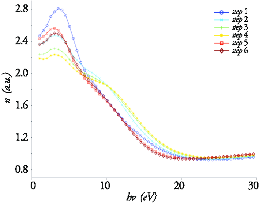
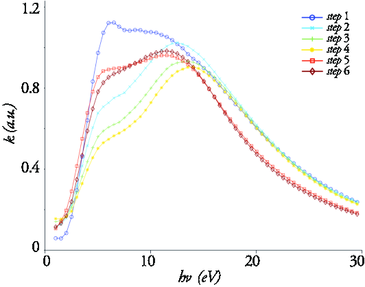
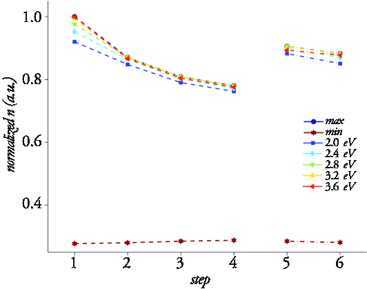
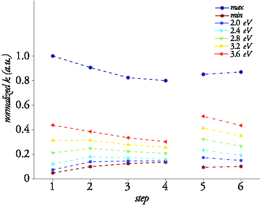
Under the former assumption, the computed results show similar behaviour for and to that observed for and , with the peak of the refractive index, , reducing by after an irradiation time of . The minimum change takes place at where the reduction is . For energies close to the band-gap the reduction is on average . The absorption, , also shows a striking decay, down to from its peak value, and a minimum of , with an average reduction of for dispersion energies close to the band-gap. Calculation of the extrema of the refractive index and absorption coefficient are shown in figures 8a and 8b.
The observed measurements, and the calculated optical properties therein, are extraordinary, in the sense that all previously published experiments, with high energy electrons (), reported an increase in the refractive index between to Suhara1975 ; Nishihara1978 ; Nordman1996a ; Nordman2001a ; Nordman2001 ; Tanaka1997a . In contrast to the vast literature reporting photon-induced refractive index change, which has yielded as much as an increase in the refractive index of As2S3 film under illumination DeNeufville1974 ; Tanaka2009 , in our experiment the refractive index decreases as much as . Bearing in mind that the conditions in the cited experiments are significantly different from those reported here, we believe the discrepancy could be explained by two different mechanisms. The first would state that, as described in the previous section, the permeability remains unchanged, while the number of electrons and the number of homopolar and broken heteropolar bonds increases; leading to the recombination mechanism described earlier. These structural alterations, in turn, induce nano-crystallization, ultimately leading to the generalized reduction in the number of energy traps, especially within energies in range A; all these simultaneous changes will cause reduction in the permittivity, and therefore reduce the refractive index.
On the other hand, to reconcile previous published results with ours, it would be necessary to acknowledge a dynamic change of the permeability with respect to electron irradiation. This would require the electrons to alter the atoms intrinsically by means of elastic collisions, and/or induce current loops, causing the magnetic dipoles in the material to reorganize, so inducing paramagnetic states, and hence increasing the permeability. However plausible the latter explanation, an experimental confirmation is required, together with further studies on the permeability of chalcogenide glass under high energy electron- and photon- irradiation.
IV Conclusions
A new characterization procedure and analysis of the permittivity of As2S3 chalcogenide glass has been presented based on low-loss Electron Energy Loss Spectroscopy. The results are extendable to the optical regime by means of the small angle scattering approximation. Furthermore, they allow us to calculate an approximate form of the refractive index, assuming constant permeability, and suggest the possibility of magnetic alterations induced by electron irradiation.
The calculated results and observations found that high energy electrons induced a reduction in the permittivity, real and imaginary, of As2S3 thin film. The real permittivity underwent a maximum reduction of , while the imaginary permittivity decreased by . The results can be explained in terms of the atomic bond reconfiguration; in this model the incident electrons break the homopolar and heteropolar bonds, leading to a reduction of the former, correcting the wrong bonds.
The results are significant to the development of manifold photonic applications, with applications to numerous areas of research and engineering. Namely, the observed reduction in the permittivity could enable a new range of transformation optic devices, which have been so far limited to the realm of far-IR range of the electromagnetic field. Furthermore, these results could be significant to future implementation of reconfigurable photonic circuits, infrared telecommunications, photonic crystals, and all optical conversion and computing.
Acknowledgements
The authors wish to acknowledge Erica T. Jolly , Alfonso Caraveo, and Carlos Argaez for their suggestions, corrections and valuable discussions in preparing this manuscript.
References
- (1) Z. Yang, M. K. Fah, K. A. Reynolds, J. D. Sexton, M. R. Riley, M.-L. Anne, B. Bureau, and P. Lucas, “Opto-electrophoretic detection of bio-molecules using conducting chalcogenide glass sensors,” Optics Express, vol. 18, p. 26754, Dec. 2010.
- (2) B. J. Eggleton, B. Luther-Davies, and K. Richardson, “Chalcogenide photonics,” Nature Photonics, vol. 5, pp. 141–148, 2011.
- (3) M. D. Pelusi, F. Luan, S. J. Madden, D.-y. Choi, D. Bulla, B. Luther-Davies, and B. J. Eggleton, “Chalcogenide Glass Chip Based Nonlinear Signal Processing - OSA Technical Digest (CD),” in Integrated Photonics Research, Silicon and Nanophotonics, p. IWC3, Optical Society of America, July 2010.
- (4) B. J. Eggleton, “Chalcogenide photonics: fabrication, devices and applications Introduction,” Optics Express, vol. 18, p. 26632, Dec. 2010.
- (5) C. Xiong, L. G. Helt, A. C. Judge, G. D. Marshall, M. J. Steel, J. E. Sipe, and B. J. Eggleton, “Quantum-correlated photon pair generation in chalcogenide As_2S_3 waveguides,” Optics Express, vol. 18, p. 16206, July 2010.
- (6) X. Bendaña, A. Polman, and F. J. García de Abajo, “Single-photon generation by electron beams.,” Nano letters, vol. 11, pp. 5099–103, Dec. 2011.
- (7) S. Juodkazis, T. Kondo, and H. Misawa, “Three-dimensional recording and structuring of chalcogenide glasses by femtosecond pulses,” in Proceedings of SPIE, vol. 5662, pp. 179–184, SPIE, Oct. 2004.
- (8) G. Chen, H. Jain, M. Vlcek, and A. Ganjoo, “Photoinduced volume change in arsenic chalcogenides by bandgap light,” Phys. Rev. B, vol. 74, p. 174203, 2006.
- (9) M. I. Kozak, V. Y. Loya, N. P. Golub, and M. Y. Onisâeurotexttrademarkko, “Mechanism of photoinduced nanodimensional expansion/contraction in glassy thin layers of As2S3,” Theoretical and Experimental Chemistry, vol. 45, pp. 69–73, May 2009.
- (10) H. Fritzsche and H. Firtzsche, “Photo-induced fluidity of chalcogenide glasses,” Solid State Communications, vol. 99, no. 3, p. 153, 1996.
- (11) K. Tanaka, “Photoinduced deformations in chalcogenide glasses: scalar and vectorial,” Journal of Optoelectronics and Advanced Materials, vol. 7, no. 5, pp. 2571 – 2580, 2005.
- (12) J. Feinleib, J. P. DeNeufville, S. C. Moss, and S. R. Ovshinsky, “Rapid reversible light-induced crystallization of amorphous semiconductors,” Applied Physics Letters, vol. 18, p. 254, Oct. 1971.
- (13) K. Tanaka and K. Shimakawa, “Chalcogenide glasses in Japan: A review on photoinduced phenomena,” physica status solidi (b), vol. 246, pp. 1744–1757, Aug. 2009.
- (14) I. Istvan, Photo- and ion-induced changes in amorphous chalcogenide films. PhD thesis, Debrecen, 2007.
- (15) J. De Neufville, S. Moss, and S. Ovshinsky, “Photostructural transformations in amorphous As2Se3 and As2S3 films,” Journal of Non-Crystalline Solids, vol. 13, no. 2, pp. 191–223, 1974.
- (16) V. Gopal, “Energy gap-refractive index interrelation,” Infrared Physics, vol. 22, no. 5, pp. 255–257, 1982.
- (17) R. M. Kurtz, W. Lu, J. Piranian, T. Jannson, and A. O. Okorogu, “The Fast Photorefractive Effect and Its Application to Vibrometry,” Journal of Holography and Speckle, vol. 5, pp. 149–155, Aug. 2009.
- (18) V K Tikhomirov and S R Elliott, “The anisotropic photorefractive effect in bulk As 2 S 3 glass induced by polarized subgap laser light,” Journal of Physics: Condensed Matter, vol. 7, no. 8, p. 1737, 1995.
- (19) M. Kowalyshen, Photoinduced Dichroism in Amorphous As2Se3 Thin Film. PhD thesis, 2010.
- (20) V. G. Ta’eed, M. R. E. Lamont, D. J. Moss, B. J. Eggleton, D.-Y. Choi, S. Madden, and B. Luther-Davies, “All optical wavelength conversion via cross phase modulation in chalcogenide glass rib waveguides.,” Optics express, vol. 14, pp. 11242–7, Nov. 2006.
- (21) V. Lyubin, M. Klebanov, M. Veinger, I. Lyubina, and B. Sfez, “Photoluminescence and photostructural transformations in neodymium-doped glassy chalcogenide films,” Optical Materials, vol. 28, pp. 1115–1117, June 2006.
- (22) P. Anderson, “Model for the electronic structure of amorphous semiconductors,” Physical Review Letters, vol. 34, no. 15, pp. 953–955, 1975.
- (23) H. Fritzsche, “Toward understanding the photoinduced changes in chalcogenide glasses,” Semiconductors, vol. 32, pp. 850–854, Aug. 1998.
- (24) S. Simdyankin, S. Elliott, Z. Hajnal, T. Niehaus, and T. Frauenheim, “Simulation of physical properties of the chalcogenide glass As2S3 using a density-functional-based tight-binding method,” Physical Review B, vol. 69, Apr. 2004.
- (25) A. Andriesh, M. Iovu, and S. Shutov, Semiconducting Chalcogenide Glass II - Properties of Chalcogenide Glasses, vol. 79 of Semiconductors and Semimetals. Elsevier, 1st ed., 2004.
- (26) J. Singh and K. Tanaka, “Photo-structural changes in chalcogenide glasses during illumination,” Journal of Materials Science: Materials in Electronics, vol. 18, pp. 423–428, Mar. 2007.
- (27) T. Suhara, H. Nishihara, and J. Koyama, “Electron-Beam-Induced Refractive-Index Change of Amorphous Semiconductors,” Japanese Journal of Applied Physics, vol. 14, pp. 1079–1080, July 1975.
- (28) N. Nordman and O. Salminen, “Thickness variations in amorphous As2S3 films induced by electron beam,” Solid State Communications, vol. 100, pp. 241–244, Oct. 1996.
- (29) N. Nordman and O. Nordman, “Refractive index change caused by electron irradiation in amorphous As–S and As–Se thin films coated with different metals,” Journal of Applied Physics, vol. 90, p. 2206, Sept. 2001.
- (30) O. Nordman, N. Nordman, and V. Pashkevich, “Refractive-index change caused by electrons in amorphous AsS and AsSe thin films doped with different metals by photodiffusion,” Journal of the Optical Society of America B, vol. 18, p. 1206, Aug. 2001.
- (31) K. Tanaka, “Electron beam induced reliefs in chalcogenide glasses,” Applied Physics Letters, vol. 70, p. 261, Jan. 1997.
- (32) J. Perrin, J. Cazaux, and P. Soukiassian, “Optical Constants and Electronic Structure of Crystalline and Amorphous As2S3 in the 3 to 35 eV Range,” physica status solidi (b), vol. 62, pp. 343–350, Apr. 1974.
- (33) R. F. Egerton, Electron Energy Loss Spectroscopy in the Electron Microscope. New York: Plenum Press, 2nd ed., 1996.
- (34) R. H. Ritchie, “Plasmon losses by fast electron in thin films,” Physical Review, vol. 106, pp. 874–881, 1957.
- (35) P. Nozieres and D. Pines, “Electron interaction in solids: Chacteristic energy-loss spectrum,” Physical Review, vol. 113, pp. 1254–1267, 1959.
- (36) M. Stöger-Pollach, “Optical properties and bandgaps from low loss EELS: pitfalls and solutions.,” Micron (Oxford, England : 1993), vol. 39, pp. 1092–110, Dec. 2008.
- (37) R. F. Egerton, “Electron energy-loss spectroscopy in the TEM,” Reports on Progress in Physics, vol. 72, p. 016502, Jan. 2009.
- (38) J. Verbeeck and G. Bertoni, “Deconvolution of core electron energy loss spectra.,” Ultramicroscopy, vol. 109, pp. 1343–52, Oct. 2009.
- (39) F. J. García de Abajo, “Optical excitations in electron microscopy,” Reviews of Modern Physics, vol. 82, pp. 209–275, Feb. 2010.
- (40) L. Zhang, S. Turner, and J. Verbeeck, “Model-based determination of dielectric function by STEM low-loss EELS,” Physical Review B, vol. 81, p. 035102, Jan. 2010.
- (41) K. Hoffmann, Electron Energy Loss Spectroscopy as an Experimental Probe for the Crystal Structure and Electronic Situation of Solids. Weinheim, Germany: Wiley-VCH Verlag GmbH & Co. KGaA, Apr. 2012.
- (42) J. Ramírez-Malo, E. Márquez, C. Corrales, P. Villares, and R. Jiménez-Garay, “Optical characterization of As2S3 and As2Se3 semiconducting glass films of non-uniform thickness from transmission measurements,” Materials Science and Engineering: B, vol. 25, pp. 53–59, June 1994.
- (43) O. Nordman, N. Nordman, and N. Peyghambarian, “Electron beam induced changes in the refractive index and film thickness of amorphous As[sub x]S[sub 100−x] and As[sub x]Se[sub 100−x] films,” Journal of Applied Physics, vol. 84, p. 6055, Dec. 1998.
- (44) A. Kovalskiy, J. Neilson, A. Miller, F. Miller, M. Vlcek, and H. Jain, “Comparative study of electron- and photo-induced structural transformations on the surface of As35S65 amorphous thin films,” Thin Solid Films, vol. 516, pp. 7511–7518, Sept. 2008.
- (45) a. M. Nastas, a. M. Andriesh, V. V. Bivol, a. M. Prisakar, and G. M. Tridukh, “Effect of electric field on photoinduced changes in the optical properties of chalcogenide glassy semiconductors,” Technical Physics Letters, vol. 32, pp. 45–47, Jan. 2006.
- (46) V. Arkhipov, M. Iovu, M. Iovu, A. Rudenko, and S. Shutov, “Negative transient currents in amorphous semiconductors,” International Journal of Electronics, vol. 51, pp. 735–742, 1981.
- (47) K. Tanaka, “Chemical and medium-range orders in As2S3 glass,” Physical Review B, vol. 36, no. 18, pp. 9746–9752, 1987.
- (48) J. M. Lee, G. Pfeiffer, M. A. Paesler, D. E. Sayers, and A. Fontaine, “Photon intensity-dependent darkening kinetics in optical and structural anisotropy in a-As2S3: A study of X-ray absorption spectroscopy,” Journal of Non-Crystalline Solids, vol. 114, pp. 52–54, 1989.
- (49) H. Nishihara, Y. Handa, T. Suhara, and J. Koyama, “Direct writing of optical gratings using a scanning electron microscope,” Applied Optics, vol. 17, p. 2342, Aug. 1978.