Generation of -Bessel-Gauss Beam by an Heterogeneous Refractive Index Map
Abstract
In this paper, we present the theoretical studies of a refractive index map to implement a Gauss to -Bessel-Gauss convertor. We theoretically demonstrate the viability of a device that could be fabricated on platform or by photorefractive media. The proposed device is in length and in width, and its refractive index varies in controllable steps across the light propagation and transversal directions. The computed conversion efficiency and loss are , and , respectively. The theoretical results, obtained from the beam conversion efficiency, self-regeneration, and propagation through an opaque obstruction; demonstrate that a 2D graded index map of the refractive index can be used to transform a Gauss beam into a -Bessel-Gauss beam. To the best of our knowledge, this is the first demonstration of such beam transformation by means of a 2D index-mapping which is fully integrable in silicon photonics based planar lightwave circuits (PLC). The concept device is significant for the eventual development of a new array of technologies, such as micro optical tweezers, optical traps, beam reshaping and non-linear beam diode lasers.
Manuscript published at the Journal of the Optical Society of America A, JOSA A, Vol. 29, Issue 7, pp. 1252-1258 (2012)
I Introduction
In 1987 Durnin introduced non-diffracting Bessel beams as members of a family of solutions to the homogeneous Helmholtz equation, with distinctive properties, e.g. their transverse profile does not change as the beam propagates in free space and exhibit self-regeneration when disturbed by non-transparent obstacles 1 . Among them the zero order, , Bessel beam has captured most attention due to its peculiar intensity distribution, which is focused on the propagation axis, besides non-diffracting propagation 2 .
Whilst mathematically viable, Bessel beams are not square integrable, i.e. the beam contains infinite energy, thus, rendering the ideal solution infeasible 6 ; 26 . Yet good approximation exists, namely Bessel-Gauss beams. Introduced by Gorin et al. 26 these solutions to Helmholtz homogeneous equation resemble the ideal Bessel beam with the sole difference that they bear finite power; and, therefore, can be realized experimentally, while retaining the primordial characteristics of self-reconstruction and diffraction-free propagation for lengths of interest to many optical applications, e.g. optical tweezers and microscopy 26 ; 3 ; 4 ; 5 .
Experimentally, Durnin et al. 7 were the first to show that it is possible to generate Bessel-Gauss beams by means of a circular slit and a lens placed one focal length away. Hakola et al. 8 proposed a Nd:YAG cavity with a diffractive mirror to transform the Gauss beam from a pump laser into a Bessel-Gauss beam of arbitrary order; Arrizón et al. 9 and Otero 10 independently used holograms to alter Gauss beams and produce zero and first order Bessel-Gauss beams; lately, Zhan 11 has shown that it is possible to generate them by using a radially polarized beam and surface plasmon resonance. Alternatively Cong 2 used phase elements to generate zero order Bessel-Gauss beams. Recently novel designs have used waveguides to produced diffraction-free beams, v.gr. Canning 27 presented a Fresnel waveguide as a diffraction-free mode generator, and Ilchenko et al. 29 experimentally showed that cylindrical waveguides can produce truncated Bessel-Gauss beams; and Tsai et al. 30 showed that is possible to use an acoustic tunable lens to generate this family of beams.
The afore mentioned methods produces high quality beams. Nonetheless their design and fabrication on photonic integrated circuits (PIC) or planar lightwave circuits (PLC) would involve complex processing stpdf, rendering the integration into most PICs platforms impractical. It is a matter of debate whether resonator/waveguide designs (see for example 27 ; 29 ) could be used for this purpose. In our experience on such devices, the quality of the beam, and conversion efficiency critically depend on the coupling efficiency. Moreover the converted beam free space propagation is limited to 29 . Hence the motivation to attain a fully integrated Gauss to -Bessel-Gauss micro-convertor based on current foundry technology is justified. If viable, it could be readily integrated into semiconductor-chip-based optical elements of great importance to a manifold of optical applications. For instance they have been shown to increase the scanning resolution and tissue penetration depth of optical coherence tomography (OCT) systems by 12 .
II Problem description and modeling
In Durnin’s primordial design, an impinging Gauss beam diffracts from the surface of an axicon lens 4 ; 7 ; 13 , forming a converging wavefront and thus giving raise to the Bessel-Gauss beam. Analytically it can be described by means of diffraction at the Fresnel limit. However accurate this method could be, it presumes the outbound field to extent infinitely in the transversal direction in order to comply with the boundary conditions 4 . To avoid this complication, we will assume hereafter the output beam to be -Bessel-Gauss as defined by Gori et al. 26 , i.e. the superposition of a Gauss and -Bessel profiles.
It could be contended that only a PIC-integrable-axicon lens would suffice to achieve the desired conversion. Such lens, though, is equivalent to the fabrication of a continuous alteration of the index of refraction, albeit homogeneous, over a conic volume, posing practical and non-trivial integration problems when it is manufactured using the well-established silicon fabrication technologies, namely the difficulty to shape the conic surface. To alleviate this conundrum, we seek a practical profile of the refractive index that can act as feasible substitute for the axicon lens, suited for integration into current silicon foundry and manufacturing technologies.
Before proceeding any further, it is important to remark that non-singular graded refractive indexes (GRIN) cannot yield perfect non-diffracting beams as proven by Hayata 28 . However a refractive index mapping can potentially achieve high quality conversion from a Gauss beam to a -Bessel-Gauss beam, which is different from the fundamental Bessel beam presented by Durnin et al. 1 .
.
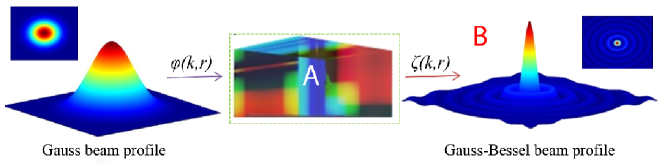
In Figure 1, the input and output beams are known a priori, and hence the problem is reduced to determining the heterogeneous refractive index in region , which will result in the transformation of the input to output fields in region . This is the optical inverse scattering problem 14 ; 15 ; 16 ; 25 .
Analytically, the input and output fields are described by harmonic functions of the form and , respectively; where and are solutions to the homogeneous Helmholtz equation. In the transformation region, medium , the field is ; where is determined by the optical properties of the medium. If the material is linear, then , and the problem narrows to determining the shape of the permittivity, , and permeability, , that realize the transformation after some finite propagation distance, .
In reality, the manipulation of permeability, , is complex. On that account the transformation medium is set to be non-magnetic, with some constant value for . Consequently, Maxwell’s equation for the electric field for this region is written as:
| (1) |
where , the permittivity, is a real value function and describes a position vector in the transformation space. Outside the device the material is homogeneous, i.e. for all , where both Gaussian and Bessel functions are well known solutions to equation 1. Inside the device, the permittivity is limited to the range achievable in practical fabrication methods:
| (3) |
Observe that if the field is given, then the only unknown in equation 3 would be , which is the permittivity map that we wish to determine. Henceforth let us examine .
Denote by and , the boundary surfaces between region A, and the incident and exit surfaces, respectively. Then can be split into the three regions:
| (4) |
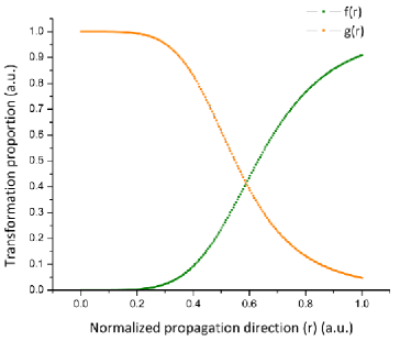
where is the transforming field. Since we wish to control , and thence decrease the complexity of the problem, we define the shape of across region . Accordingly, we introduce the real valued functions and , continuous and square integrable, i.e. smooth functions. These functions are invoked to describe the transforming beam as a superposition of the desired input and output fields, in addition to an arbitrary field that can be thought to represent the residual beam. The field can be written now as:
| (5) |
to comply with the boundary condition and . Then substituting equation 5 into equation 3 results in a second order partial differential equation:
| (6) |
Recalling vector calculus identities, the right hand side of equation 6 can be reduced to:
| (7) |
Observe that in equation 6, and are vector functions with known values across the three domains previously described (see equation 4). Thus by means of equation 7 we can rewrite equation 6 as a differential equation that describes the permittivity, , as:
| (8) |
This is the nonlinear equation for the permittivity that we ought to solve within the boundary conditions and fabrication limitations defined earlier: constant permeability, , refractive index range , where ; and fabrication minimum feature size .
The computation of an inverse problem as the one hitherto described by equation 8 is not trivial, and analytical solutions are rarely found. Moreover, the problem described by the above equation is non-linear and ill-defined, i.e. its solution is not unique and is dependent continuously on the data 17 ; 31 . As a result, many numerical schemes have been developed to elucidate the solution, v.gr. the adjoint problem 14 ; 17 , linear sampling 18 ; 19 ; 20 , variational methods 21 , and lately transformation optics 22 ; 23 ; 25 . To find a solution to this quandary, we developed a numerical technique based on the variational method and the adjoint problem.
We begin by noting that if the input and output beams are symmetrical around the propagation axis , and does as well the field in the transformation region, then we can scale down the problem to two-dimensions: and , the longitudinal and transversal direction, respectively. Concerning our matter at hand both Bessel and -Bessel-Gauss beams are symmetric around the propagation axis; moreover the transformation field as described by the above equations is also symmetric around the axis . Therefore, our problem can be scaled down to a two dimensional numerical scheme.
Accordingly, the simulation space is discretized on a grid size by . The solver is given an initial guess of the permittivity map across the region at every point . The solution to equation 3 is computed via a variational approach as described in 21 : at every point the transversal function of is determined by solving equation 8 to the boundary conditions (see equation 5): and ; and the field at that point . This iterative approach is carried for every point . Thus the transversal shape of , and consequently that of , is determined to match the resulting field to the ideal transformation given by equation 5.
This method solely does not guarantee that the solution will be exempted of extreme or singular values, withal the variational method is especially sensitive numerical approximations 21 . To account for the latter and work out the extrema in the refractive index, we implement a solution coming from the adjoint problem 17 . The extreme and singular values are approximated to the closest value in the defined range. We then propagate the initial Gauss beam through the device and determine how much the field at every point diverges from the ideal transformation of equation 5, including as well the near and far fields. An iterative refinement on this grid regions follows, as described in 14 ; 17 , to match the numerical computation output to the ideal -Bessel-Gauss beam. The beam propagation method is used to propagate the initial Gauss beam through the heterogeneous region .
It is important to note that both, the variational and adjoint problem methods, while widely tested may render inexact solutions due to numerical approximations which can lead to instability and are in general related to the limited resolution of any numerical method. To counterweight this difficulties the general approach is to use smaller grid sizes even at the expense of computational time increasing exponentially.
III Results.
The transformation functions and are plotted in Figure 2b. The initial guess for the permittivity map is a Gaussian profile in the transversal direction for all points along , width and a maximum peak of or . The initial beam in region follows a Gaussian function, with width and normalized energy to unity.
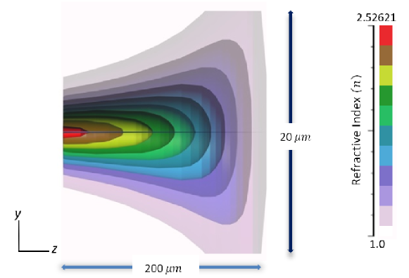
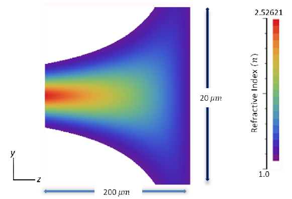
The outcome of the calculation and optimization process described earlier is depicted in the schematized Figure 3 and the fine resolution () plot of the refractive index in Figure 4. The refractive index map is symmetric around the propagation axis , and is comprised of a smooth variation of the refractive index between and . The minimum feature size, , is , and has the final dimensions length by wide. Notice that the minimum feature size defines the smoothness of the refractive index map.
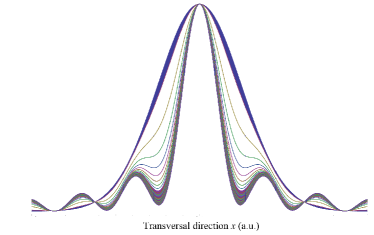
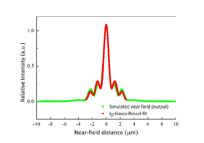
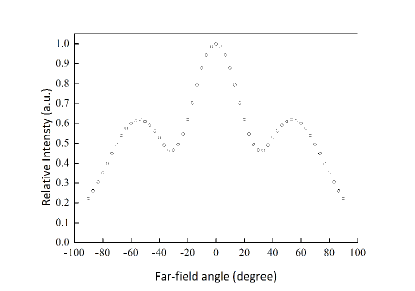
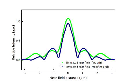
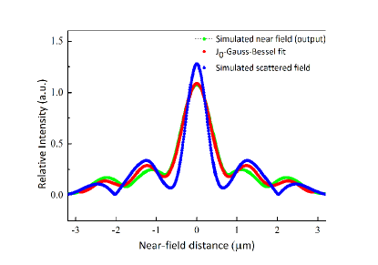
The initial impinging Gauss beam in region propagates through the device in region , and it is transformed into a -Bessel-Gauss beam with a efficiency. Figure 5a shows the results for the field at from the exit of the device, with the corresponding far field depicted in Figure 5b. As described earlier, this is the optimized value considering the current state-of-the-art nano-fabrication techniques and facilities available to realize the device.
In Figure 5, it is observed that both near and far fields follow a -Bessel-Gauss profile with accuracy. The converted beam divergence is less than after propagating and less than after traveling . The energy density at the principal peak is of the converted beam’s total energy, which makes it ideal for OCT applications and free space light-based communication. Losses due to material absorption, scattering and back reflections are of the incident field, or , which can be significantly reduced by using antireflection coatings at the input and output surfaces.
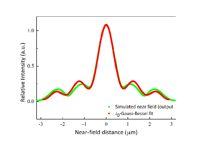
Within the known limitations in fabrication processes, it is noted that not all values of the index of refraction can be achieved. A theoretical study is required to define the tolerance to minimum feature size and its repercussions in the beam profile. We study this case by further modifying the grid size, i.e. the minimum feature size, from to . The results are shown in Figure 6.
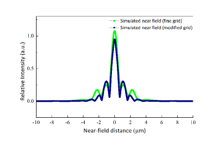
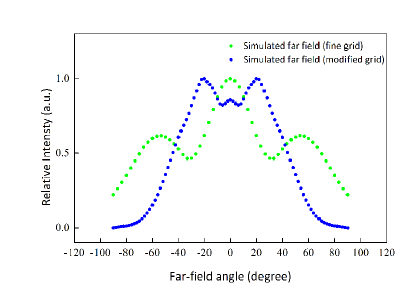
As it is evident from Figure 6a, modifying the refractive index grid size results in a beam that also resembles a -Bessel-Gauss beam with a accuracy, with the sole difference that this beam as it propagates will evolve into a non-Bessel-Gauss beam. This can be drawn from the far field, plotted in Figure 6b. Observe that at infinity the field no longer corresponds to the far field of a -Bessel-Gauss beam. Nevertheless, a coarse mapping will produce a highly focused beam, where of the energy is localized at the first peak, and the beam diffraction over propagation is less than .
Bessel-Gauss beams, alike Bessel beams, exhibit self regeneration when their path is perturbed by a non- transparent scatterers. To examine this self-healing property of the outbound -Bessel-Gauss beam, we insert a random index medium on its propagation path.The results are shown in Figure 7.
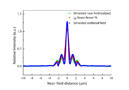
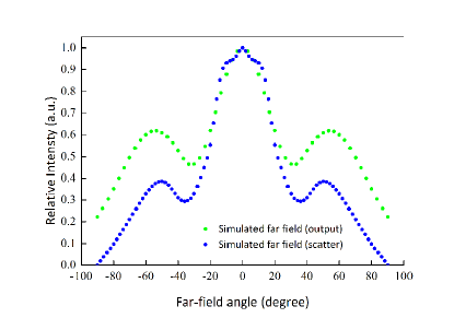
The generated -Bessel-Gauss beam is made to impinge on a random index media, which consists of a circle-like region of , set at from the output of the device, and refractive index of . The scatterer partially obstructs the propagation of the beam. The scattered beam profile is computed at from the alien obstruction (see Figure 7a and its magnified version in Figure 7c), as well as the far field (see Figure 7b). As can be seen from the results in Figure 7, the beam described earlier (see Figure 5) exhibits self-regeneration. The divergence, computed by comparing the width of the principal peak, from the scattered field to the original transformed beam is . Since the beam is not a full Bessel beam, some light is scattered by the object, as expected, giving rise to a loss of or .
The 2D mapping for beam conversion heretofore described while challenging to fabricate, could be built using current nano-manufacturing techniques. A prototype, verbi gratia, could be obtain by controlling the degree of oxidation in 32 ; 33 systems, or by horizontally stacking nano-layers of photo-refractive materials such as chalcogenide glasses which have been shown to have a wide range of refractive index 34 ; 35 . The advantages of these materials are that they are relatively well-developed, and the material systems are compatible with PICs and PLCs.
IV Conclusions
We have, to the best of our knowledge, theoretically demonstrated the viability of the first PIC and PLC compatible device utilizing a heterogeneous refractive index map, to achieve the transformation of a Gauss beam into a -Bessel-Gauss beam. The computed device has a loss of , and high energy focus, where of the output beam energy is concentrated at the principal peak of the -Bessel-Gauss beam profile. The beam has a divergence of over a propagation distance of , and exhibits self-healing when partially obstructed by an opaque object. The resulting beam has a -Bessel-Gauss profile for both near- and far-fields. It is note that our design is based on current manufacturing techniques, such as controlled oxidation of or by stacking different layers of chalcogenide glasses. An integrated Gauss to -Bessel-Gauss beam convertor could enable on-chip applications which take advantage of the beam’s self-healing and non-diffractive properties, such as micro optical tweezers, traps and couplers, photonic integrated circuits for telecommunications and computerized micro tomography and microscopy.
References
- (1) J. Durnin, “Exact solutions for nondiffracting beams. I. The scalar theory”, J. Opt. Soc. Am. A 4, 651 (1987).
- (2) W. Cong, N. Chen, and B. Gu, “Generation of nondiffracting beams by diffractive phase elements”, J. Opt. Soc. Am. 15, 2362 (1998).
- (3) S. Chavez-Cerda, “A new approach to Bessel beams”, J. Modern Optics 46, 923 (1999).
- (4) F. Gori, G. Guattari, and C. Padovani, “Bessel-Gauss beams”, Opt. Commun. 64, 491 (1987).
- (5) Y. Lin, W. Seka, J. H. Eberly, H. Huang, and D. L. Brown, “Experimental investigation of Bessel beam characteristics”, Appl. Opt. 31, 2708 (1992).
- (6) R. M. Herman and T. A. Wiggins, “Propagation and focusing of Bessel-Gauss, generalized Bessel-Gauss and modified Bessel-Gauss beams”, J. Opt. Soc. Am. A 18, 170 (2001).
- (7) I. A. Litvin, M. G. McLaren, and A. Forbes, “Propagation of obstructed Bessel and Bessel-Gauss beams”, Proc. SPIE 7062, 706218 (2008).
- (8) J. Durnin, J. Jr. Miceli, and J. H. Eberly, “Diffraction-free beams”, Phys. Rev. Lett. 46, 1499, (1987).
- (9) F. Wu, Y. Chen, and D. Guo, “Nanosecond pulsed Bessel-Gauss beam generated directly from Nd:YAG axicon-based resonator”, Appl. Opt. 46, 4943 (2008).
- (10) V. Arrizón, D. Sánchez-de-la-Llave, U. Ruiz, and G. Méndez, “Efficient generation of an arbitrary nondiffracting Bessel beam employing its phase modulation”, Opt. Lett. 34, 1456 (2009).
- (11) M. M. Méndez Otero, G. C. Martínez Jiménez, M. L. Arroyo Carrasco, M. D. Iturbe Castillo, and E. A. Martí Panameño, “Generation of Bessel-Gauss beams by means of computed generated holograms for Bessel Beams”, in Frontiers in Optics, OSA Technical Digest (CD) (Optical Society of America, 2006), paper JWD129.
- (12) Q. Zhan, “Evanescent Bessel beam generation via surface plasmon resonance excitation by radially polrized beam”, Opt. Lett. 31, 1726 (2006).
- (13) J. Canning, “Diffraction-free mode generation and propagation in optical waveguides”, Opt. Commun. 207, 35 (2002).
- (14) V. S. Ilchenko, M. Mohageg, A. A. Savchenkov, A. B. Matsko, and L. Maleki, “Efficient generation of truncated Bessel beams using cylindrical waveguides”, Opt. Express 15, 5866 (2007).
- (15) T. Tsai, E. McLeod, and C. B. Arnold, “Generating Bessel beams with a tunable acoustic gradient index of refraction lens”, Proc. SPIE 6326, 63261F (2006).
- (16) F. O. Fahrbach, P. Simon, and A. Rohrbach, “Microscopy with self-reconstructing beams”, Nature Photonics 4, 780 (2010).
- (17) M. Lei and B. Yao, “Characteristics of beam profiles of Gaussian beam passing through an axicon”, Opt. Commun. 239, 367 (2004).
- (18) K. Hayata, “Are Bessel beams supportable in Graded-Index media?”, Opt. Rev. 3, 299 (1996).
- (19) B. Gang and L. Peijun, “Inverse medium scattering problems for electromagnetic waves”, SIAM J. Appl. Math. 65, 2049 (2005).
- (20) A. J. Devaney, “A filtered backprojection algorithm for diffraction tomography”, Ultrasonic Imaging 4, 336 (1982).
- (21) R. M. Lewis, “Physical Optics inverse diffraction”, IEEE Trans. An. Prop. 17, 308 (1969).
- (22) Y. Lai, J. Ng, H. Yang, D. Han, J. Xiao, Z. Q. Zhang, C. T. Chang, “Illusion optics: the optical transformation of an object into another object”, Phys. Rev. Lett. 102, 253902 (2009).
- (23) M. Piana, “On uniqueness for anisotropic inhomogeneous inverse scattering problems”, Inverse Problems 14, 1565 (1998).
- (24) O. Dorn, H. Bertete-Aguirre, J. G. Berryman, and G. C. Papanicolaou, “A nonlinear inversion method for 3D electromagnetic imaging using adjoint fields”, Inverse Problems 15, 1523 (2005).
- (25) A. J. Devaney, “A computer simulation study of diffraction tomography”, IEEE Trans. Biomed. Eng. 30, 377 (1983).
- (26) H. Hadar and P. Monk, “The linear sampling method for solving the electromagnetic inverse medium problem”, Inverse Problems 18, 891 (2002).
- (27) H. Hadar, “The interior transmission problem for anisotropic Maxwell’s equations and its applications to the inverse problem”, Math. Methods App. Sciences 27, 2111 (2004).
- (28) F. Cakoni, “A variational approach for the solution of the electromagnetic interior transmission problem for anisotropic media”, Inverse Problems and Imaging 1, 3 (2007).
- (29) J. B. Pendry, D. Schurig, and D. R. Smith, “Controlling electromagnetic fields”, Science 312, 1780 (2006).
- (30) U. Leonhardt and T. G. Philbin, “Transformation optics and the geometry of light”, Progress in Optics 53, 69 (2008).
- (31) H. Chen, C. T. Chan, and P. Sheng, “Transformation optics and metamaterials”, Nature materials 9, 387 (2010).
- (32) H. J. Lee, C. H. Henry, K. J. Orlowsky, R. F. Kazarinov, and T. Y. Kometani, “Refractive-index dispersion of phospho-silicate glass, thermal oxide, and silicon nitride films on silicon”, Appl. Opt. 27, 4104 (1988).
- (33) W. Fenga, W. K. Choia, L. K. Beraa, M. Jib, and C.Y. Yangb, “Optical characterization of as-prepared and rapid thermal oxidized partially strain compensated films”, Mat. Sc. Sem. Proc. 4, 655 (2001).
- (34) A. Zakery, “Optical properties and applications of chalcogenide glasses: a review”, J. Non-Crystaline Solids 330, 1 (2003).
- (35) S. B. Kang,“Optical and Dielectric Properties of Chalcogenide Glasses at Terahertz Frequencies”, ETRI Journal 31, 667 (2009).