Graphene for spintronics: giant Rashba splitting due to hybridization with Au
Abstract
Graphene in spintronics [Yazyev, ] has so far primarily meant spin current leads of high performance because the intrinsic spin-orbit coupling of its electrons is very weak [Tombros-Nature-2007, ; Shinjo09, ; Kawakami09, ]. If a large spin-orbit coupling could be created by a proximity effect, the material could also form active elements of a spintronic device such as the Das-Datta spin field-effect transistor [Das, ], however, metal interfaces often compromise the band dispersion of massless Dirac fermions [OshimaPRB92, ]. Our measurements show that Au intercalation at the graphene-Ni interface creates a giant spin-orbit splitting ( meV) in the graphene Dirac cone up to the Fermi energy. Photoelectron spectroscopy reveals hybridization with Au states as the source for the giant spin-orbit splitting. An ab initio model of the system shows a Rashba-split dispersion with the analytically predicted gapless band topology around the Dirac point of graphene and indicates that a sharp graphene-Au interface at equilibrium distance will account for only meV spin-orbit splitting. The ab initio calculations suggest an enhancement due to Au atoms that get closer to the graphene and do not violate the sublattice symmetry.
Introduction
Graphene shows fascinating electronic properties due to its structure consisting of two equivalent sublattices A and B that determine its band structure with the linear dispersion near conical and points in reciprocal space. A and B are identified as a pseudospin, and the isospin indicating and valleys is a conserved quantum number [KM05, ]. In addition to the pseudo- and isospin, also the real spin is recently being considered important in graphene [Yazyev, ; KM05, ; Huertas09, ; Trauzettel, ; Gmitra, ; Trickey, ; Semenov, ; Tombros-Nature-2007, ; Varykhalov-PRL-2008, ; Shinjo09, ; Kawakami09, ]. The main contribution to the intrinsic spin-orbit splitting originates from the coupling to graphene orbitals [Gmitra, ]. The resulting splitting is just of the order of 0.01 meV [Trickey, ] which means together with the high carrier mobilities in graphene a large spin coherence length with measured values reaching 1.5–2 m [Tombros-Nature-2007, ; Shinjo09, ; Kawakami09, ]. The theoretical predictions are even by an order of magnitude higher so that it is at present unclear whether these values represent practical limits [Huertas09, ].
We have recently measured a graphene spin-orbit splitting of meV [Varykhalov-PRL-2008, ]. This splitting occurs in the system graphene/Ni(111) after a Au layer with one atom thickness is intercalated by heating between the graphene and the Ni [ShikinPRB00, ]. This Au layer serves a dual purpose: on the one hand, it transforms the strongly bonded [OshimaPRB92, ] graphene monolayer on Ni(111) into an electronically quasifreestanding structure. This decoupling effect is apparent from the resulting linear quasirelativistic bands of the graphene, i. e., the Dirac cone [Varykhalov-PRL-2008, ; fussnote1, ].
On the other hand, the Au interlayer produces a different type of the spin-orbit splitting through an extrinsic effect. Indeed, the spin-orbit coupling is known to be important at the surface of Au [LaShell, ] and in Au nanowires [Barke06, ], and Au(111) is frequently considered a model for a Rashba effect induced by breaking up-down symmetry [LaShell, ; Henk, ]. For graphene with its 2-atom basis (sublattices A and B) and an additionally broken up-down symmetry, the band dispersion including spin-orbit coupling has been calculated in Ref. [RashbaPRB09, ]. In zero magnetic field, the dependence of the spin polarization on the two-dimensional electron wave vector k∥ was found. The band topology was predicted to be similar to that of the unbiased spinless graphene bilayer but with an additional spin texture which is tangential to the circular constant-energy surfaces. The effect couples spin and pseudospin in such a way that contributions from both A and B sublattices can lead to a substantial spin interference in the photoemission process [Kuemmeth, ].
Experiment
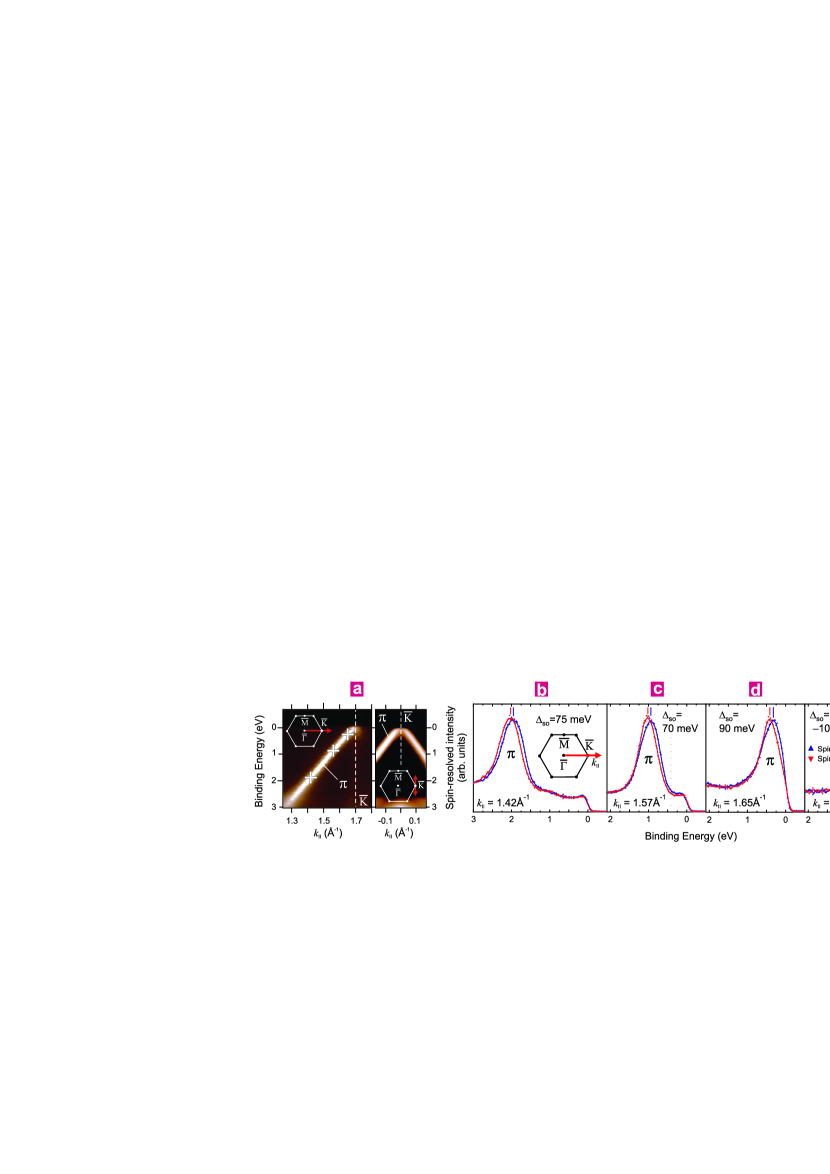
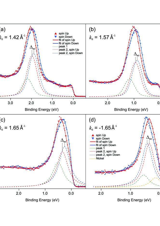
In the present Communication, we show by spin- and angle-resolved photoelectron spectroscopy that an extrinsic spin-orbit splitting of the order of 100 meV can be obtained in graphene near the Fermi energy, i. e., an enhancement by an order of magnitude relative to our previous finding [Varykhalov-PRL-2008, ]. We will show that we can very well identify the type of superstructure characterising the graphene-Au interface in good agreement with the bulk lattice constants of graphene, Au, and Ni. We determine very clearly the spin-dependent hybridization at the interface and its change with the superstructure. Based on ab initio calculations, the giant size of the spin-orbit splitting must be understood as resulting from more dilute Au at a closer distance to the carbon atoms than in a Au monolayer, either as adatoms above or below the graphene layer. Figure 1 shows spin- and angle-resolved photoemission measurements of graphene/Au/Ni(111). Part (a) shows the band with its linear quasirelativistic dispersion, and crosses indicate where spin-resolved photoemission spectra (b–d) have been measured. The splitting between spin-up spectra (upward triangles) and spin-down spectra (downward triangles) is clearly visible and amounts to 90 meV at Å-1 and meV at Å-1. Apparently, the sign of the splitting reverses with the sign of k∥, as expected for a Rashba effect. This giant spin splitting constitutes our central experimental result. The splitting exceeds also the room-temperature broadening, and together with the fact that it extends to the Fermi energy, this makes it directly relevant for transport applications. In fact, transport properties of graphene with an externally produced (Rashba-type) spin-orbit splitting have been intensively investigated in recent years [Dyrdal09, ; QSHE, ; QAHE, ] and important predictions for such a constellation of graphene have been published: the spin Hall effect [Dyrdal09, ] and the quantum spin Hall effect [KM05, ; QSHE, ] and, with an additional exchange interaction, the quantum anomalous Hall effect [QAHE, ].
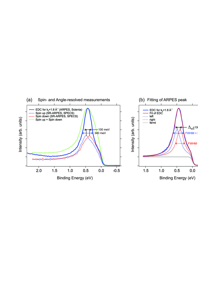
To establish connection between our previous 13 meV data and the new 100 meV data, we undertook closer inspection of the spin-resolved spectra of Fig. 1. They reveal that the system is inhomogeneous and the high-splitting phase ( meV) and the low-splitting phase ( meV) are present simultaneously. Line fits and spectral decompositions (see Supplementary Material, Fig. S5) show that the high-splitting phase makes up between one third and two thirds of the spectral weight, corresponding in the simplest picture to half of the sample region of about m that is probed simultaneously. The decomposition is possible due to an energy shift between the two phases with the low-splitting phase appearing at about 200–500 meV higher binding energy. The giant size of the splitting and the distribution in spectral weight between the high-splitting phase and the low-splitting phase ranging from to have been reproduced in several in situ preparations and at different beamlines.
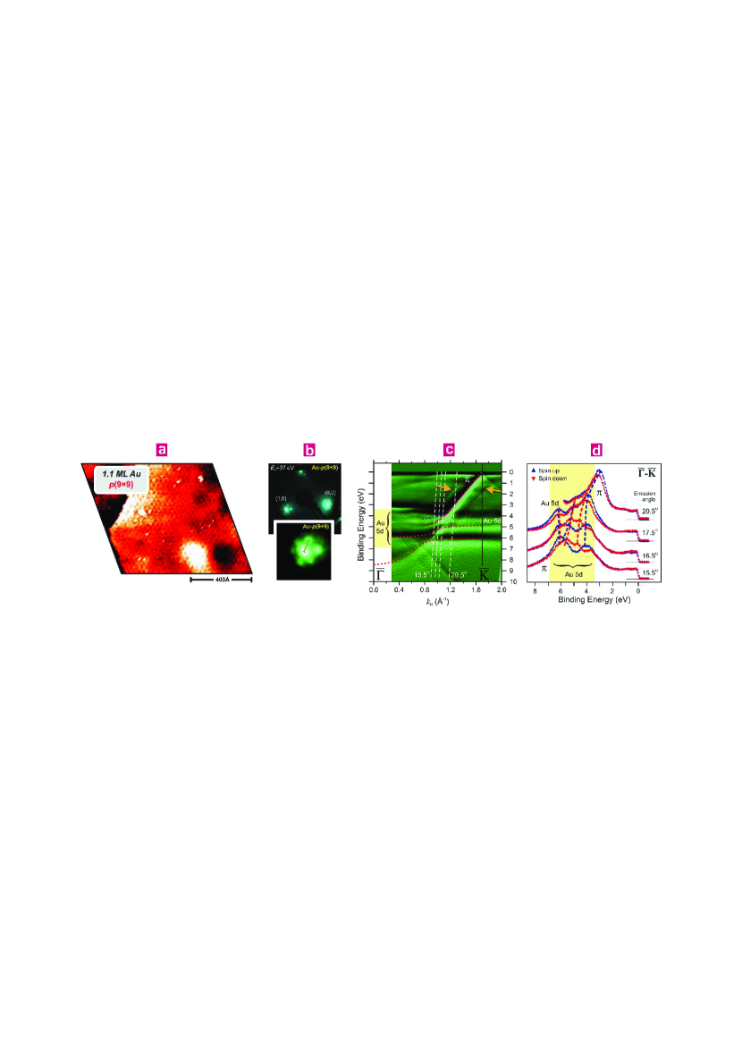
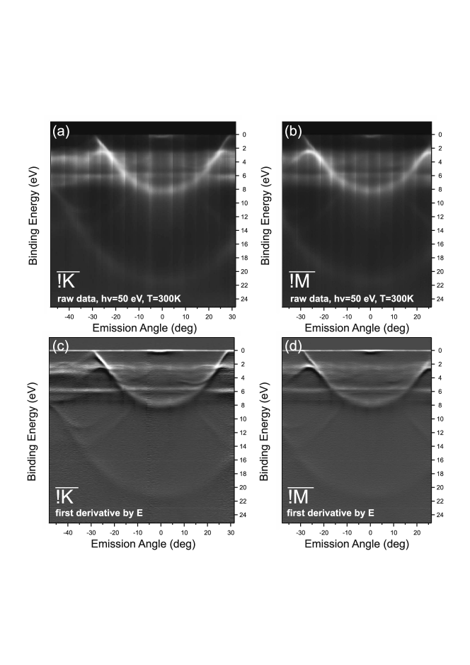
We want to unveil the electronic origin of this strongly enhanced spin splitting including the reason for its nonuniformity and the relation to our previous results. Probing as well as controlling the Au layer as the likely source of the giant Rashba splitting are challening because of its very location underneath the graphene layer. The means of control is basically through the amount of Au deposited initially (before heating) onto the graphene which typically exceeds the subsequently intercalated amount. While graphene and Ni(111) have a lattice mismatch of only 1.2%, the one between graphene and Au(111) is much larger (%). Therefore, the intercalated monolayer of Au will not reach the same atom density as the Ni. Probing the resulting structure is possible by scanning tunneling microscopy (STM) because the moiré effect reveals the superstructure through the beat frequency between the graphene lattice and the Au monolayer. Moreover, the photoemission signal from Au states under the graphene is very well visible. Figures 1a and 2c show that the graphene electronic structure resembles that of freestanding graphene. The Au layer prevents the strong carbon-Ni hybridization. Nevertheless, the graphene -states show also in the quasifreestanding phase with the Dirac cone several carbon-Au hybridization points in the range of 4 to 6.5 eV binding energy in Fig. 2c. Moreover, the orange arrows in Fig. 2c indicate further replicas of the graphene -band shifted to smaller and larger values of the wave vector k∥. The shift of k∥ amounts to between and of the distance . The STM image in Fig. 2a reveals a moiré pattern of similar periodicity but it can most accurately be determined from the superstructure in the low-energy electron diffraction (LEED) pattern as a superstructure — in good agreement with the shift of the replica bands in photoemission.
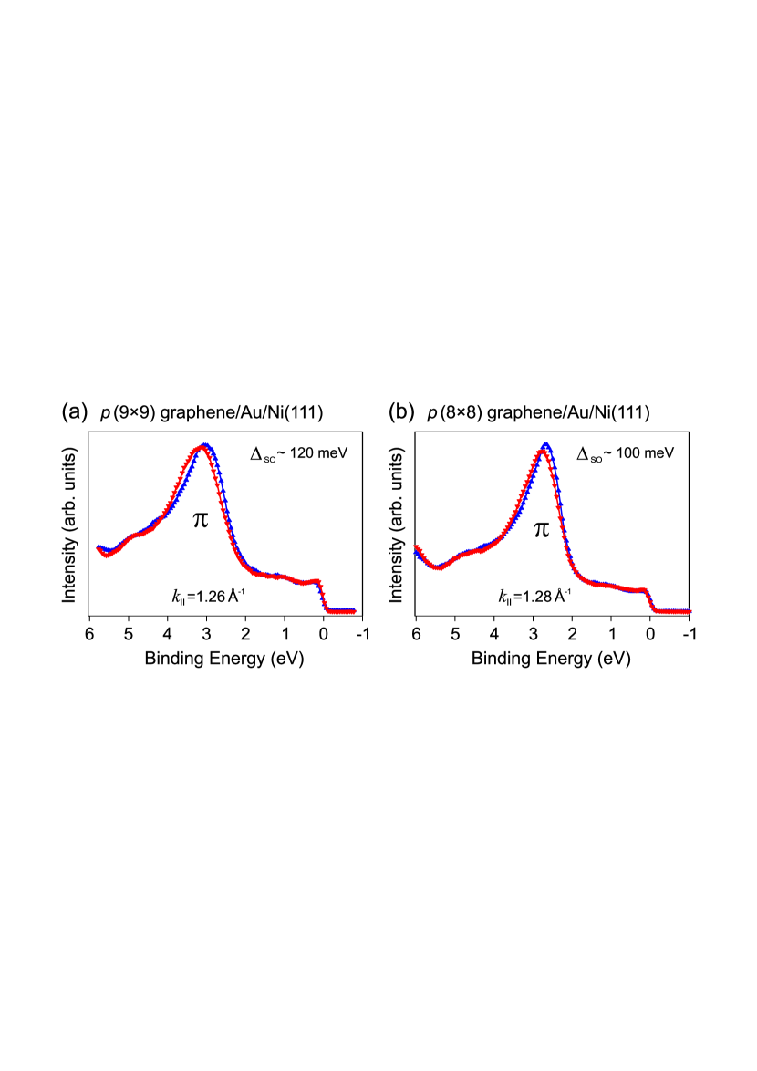
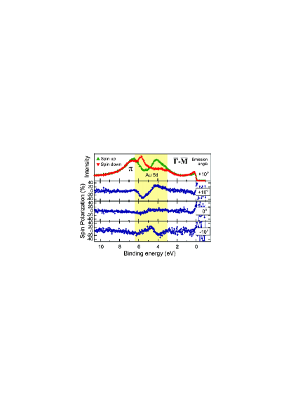
Dashed lines in Fig. 2c show where we probed the hybridization points by spin-resolved spectra (Fig. 2d). These spectra reveal that the giant spin splitting of the -band smoothly merges into an even larger spin splitting ( eV) of the Au states. This is strong indication that this spin-dependent C-Au hybridization with the heavy Au is the source of the giant Rashba splitting in the graphene.
Interestingly, when more Au is initially deposited, it forms after the intercalation a slightly different superstructure. The Supplementary Material (Fig. S1) shows that it is characterised by an extra hybridization with other Au states in the -band. This hybridization does not enhance the giant spin-orbit splitting further (Fig. S6), which indicates already that the differences between the and superstructures do not play a role for the giant spin-orbit splitting.
Theory
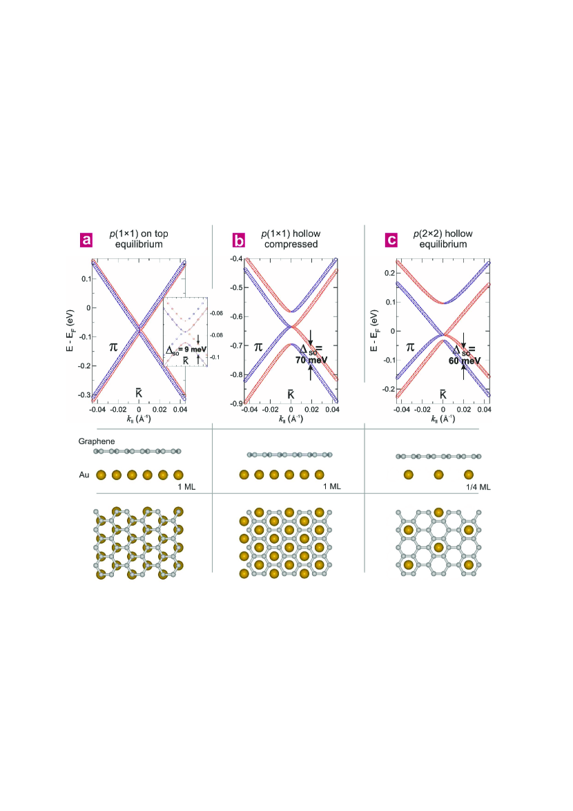
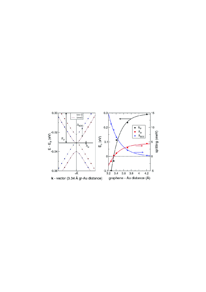
We want to turn to ab initio theory in order to verify the giant spin splitting. Modelling the or superstructure of graphene/Au, which would increase the unit cell by two orders of magnitude over that of graphene, is unnecessary because of the similar spin-orbit splitting for the two superstructures. A structure and on-top position for graphene on 1 monolayer (ML) Au has instead been chosen (Fig. 3a).
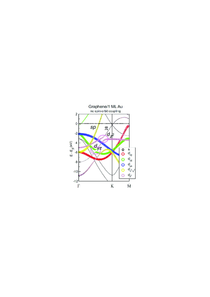
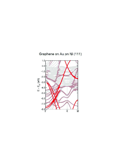
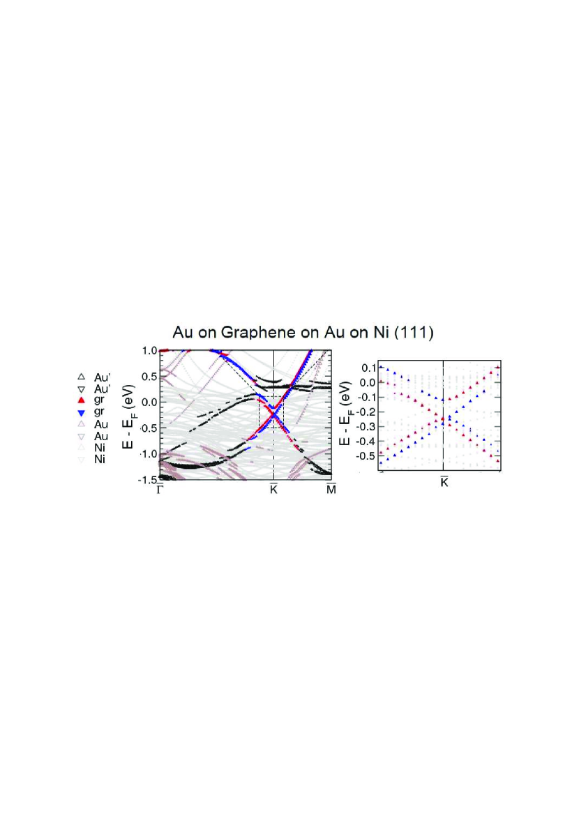
The distance between the graphene and Au monolayer is a parameter of enormous influence on the spin-orbit splitting of the graphene. The fact that also the Fermi energy varies characteristically with this distance allows us to connect to the experiment: The experimental Fermi level corresponds with its slight -doping (hole doping) to 3.3–3.4 Å in the theoretical model, and this data is shown in Fig. 3a. 3.3 Å is also the equilibrium distance calculated before for graphene/Au(111) [Giovannetti-PRL-2008, ]. According to analytical prediction, the band topology is peculiar around the point with two pairs of bands — a gapped one and a non-gapped one [RashbaPRB09, ; Kuemmeth, ]. This analytical model [RashbaPRB09, ; Kuemmeth, ] does not assume any specific surface configuration. The bands have so far been confirmed for freestanding graphene in a supercell geometry by density functional theory calculations for an applied field V/nm [Gmitra, ] but not yet for the field realistically replaced by an interface to Au. This was done in Fig. 3a which shows the spin-orbit split bands at the Dirac point at for the on-top geometry. In the inset, these ab initio results (symbols) are magnified near the Dirac point and compared to the dispersion of the analytical model (solid line), which is fully confirmed. This is also important for the predicted magnetic-field dependence [RashbaPRB09, ]. In agreement with the experiment, our ab initio calculation reveals C-Au hybridization as the source of the spin-orbit splitting in the graphene. The graphene -band ( orbitals) hybridizes indeed with the deeper Au bands of and type because of their matching symmetry. Despite the large distance of 3.3 Å the hybridization is strong which has not been considered in the literature in connection with graphene-noble-metal interfaces. This is best seen after the spin-orbit coupling is turned off leaving only gaps caused by hybridization: we determine hybridization gaps of widths eV and eV (see Fig. S11). Their absolute binding energies do not compare well to the experiment revealing the limitations of the Au monolayer as model substrate. This situation improves largely and the main C-Au hybridization moves from eV to eV below when the Ni substrate is included in the calculation (see Fig. S12).
The spin-orbit splitting in Fig. 3a is 9 meV near but increases strongly when the distance between graphene and Au is reduced (see Fig. S10 for the detailed behaviour with the distance). On the other hand, the Dirac cone is destroyed at closer graphene-Au distance, giving, e. g., for 2.5 Å a band gap at of 40 meV. The reason for this is the broken A-B symmetry of carbon atoms in the on-top geometry (Fig. 3a) which, remarkably, does not manifest itself very much at larger distances. A hollow-site geometry, instead, preserves the A-B symmetry in the graphene, see Fig. 3b. Consequently, an intact Dirac cone is obtained in the hollow-site geometry also for smaller graphene-Au distances such as 2.5 Å in Fig. 3b. We are very well able to obtain at this arbitrary interlayer distance of 2.5 Å a giant spin-orbit splitting of meV. However, such close distance costs as much as 1 eV relative to the equilibrium separation and is thus unrealistic. While the giant spin-orbit splitting apparently is difficult to reproduce by density functional theory in equilibrium, the intact Dirac cone is not. The intact Dirac cone is presently obtained with on-top graphene/Au and has also been found for graphene/Cu(111) where the on-top position is determined to be energetically favourable [Giovannetti-PRL-2008, ]. Relative to this on-top geometry which implies maximum A-B symmetry breaking, a moiré superstructure such as the one necessarily breaks the A-B symmetry to a lesser or vanishing degree which is favourable for obtaining an intact Dirac cone. After having investigated other laterally shifted positions of the overlayer and a moiré superstructure as well as corrugation in the graphene all yielding spin-orbit splittings of the order of 10 meV at equilibrium graphene-Au distances, the conclusion is that the giant spin-orbit splitting will not be accounted for by the sharp graphene-Au interface alone that our structural characterization by LEED and STM suggests as simplest case. This means that a model for a realistic splitting will have to include individual Au atoms which then can obtain a higher coordination to the carbon and due to the resulting attraction and shorter distance exert a stronger spin-orbit coupling on the graphene -states. As seen above, critical is at small graphene-Au separations the preservation of A-B symmetry which leads us once again to the hollow site geometry. Figure 3c shows this situation for graphene/0.25 ML Au in a structure with the Au in the hollow site relative to the graphene. The vertical distance of the Au to the graphene layer is 2.3 Å which (as distinct from the Au monolayer of Fig. 3b) is near the equilibrium determined by our structural optimization. Figure 3c shows that this structure enhances the spin-orbit splitting to values between 50 and 100 meV while keeping the characteristic band topology and the Dirac point. This demonstates that our experimental results are also plausible theoretically.
The and structures will include in the simplest case a substantial amount of Au atoms arranged in the hollow sites of graphene [VarykhalovPRB10, ] but this does not imply a reduced distance, especially if one considers that is also the structure which a Au monolayer alone forms on Ni(111) [Jac95, ]. Therefore, the and superstructures are probably not relevant for the giant splitting and both give rise to only meV splitting.
The previously measured data [Varykhalov-PRL-2008, ] were characterized by a smaller meV spin-orbit splitting, and this low-splitting phase is principally in agreement with our present calculations for the full Au monolayer. The published [Varykhalov-PRL-2008, ] band dispersion measured along reflects the presence of a sample with structural defects. It contained substantial contributions of rotated domains visible as characteristic dispersions appearing along (see Fig. S2) which is not the case in the present data even when the amount of intercalated Au is varied systematically from zero to more than 1 ML (see Fig. S1). The intercalation process under the graphene, including that of Au, is a present far from understood. The accepted main route is via defects in the graphene [Tontegode, ], and for large molecules this can be confirmed by STM directly [VarC60, ]. The presence of many domain boundaries facilitates the intercalation and apparently results in the low-splitting phase. Intercalation of Au works, however, also in samples which are free of defects over large distances. The temperature of intercalation and that of the initial graphene formation are very similar in the graphene/Au/Ni(111) system so that an opening and closing of the graphene appears possible during intercalation. This could lead to more Au locally closer to the graphene, either as subsurface Au or as adatoms.
The plot of Fig. 3c is useful for demonstrating that an enhancement of the spin-orbit coupling in graphene by sparsely distributed Au atoms is possible in an equilibrium structure but it does not imply that the Au arrangement possesses such an ordered structure. We can exclude that the Au atoms substitude carbon atoms. Their size would correspond to two carbon atoms and the resulting distortion would manifest itself in STM. Another possibility are non-intercalated residual atoms above the graphene for which we have no direct experimental evidence. We mention that such atoms cannot be detected by our STM technique because they should be highly mobile on graphene and shifted along by the STM tip. In order to explore a realistic model which includes the Ni substrate, the band dispersion for a structure of graphene sandwiched between 0.25 ML Au and 1 ML Au on top of 3 ML Ni has been calculated as well (Fig. S11) and gives practically the same Dirac cone with giant spin splitting as in Fig. 3c.
Summary
In summary, we report a giant Rashba splitting in graphene in contact with Au up to 100 meV that is caused by graphene-Au hybridization. A flat Au monolayer can account for only meV spin-orbit splitting as has been reported in Ref. [Varykhalov-PRL-2008, ], whereas a structure including laterally more separated Au adatoms residing in hollow-site positions closer to graphene, gives at the equilibrium graphene-Au distance rise to the enhanced splitting of – meV, a realistic Fermi level position, and an intact Dirac cone. We attribute simultaneous presence of both 100 meV and 10 meV splittings to the coexistence of areas without and with extra Au either as adatoms or immersed into the graphene.
Methods
Methods
Angle-resolved spectra have been measured with a hemispherical analyzer and parallel angular detection and a 6-axes automated manipulator. Spin- and angle-resolved photoemission has been performed with a hemispherical analyzer coupled to a Rice University Mott-type spin polarimeter operated at 26 kV sensitive to the in-plane spin component perpendicular to k∥. Linearly polarized synchrotron light from the UE112-PGM undulator beamlines at BESSY II has been used for excitation. The unmagnetized Ni(111) surface was prepared as a 15–20-ML thick film on W(110), and graphene was synthesized by cracking of propene at the Ni(111) surface held at K. Because the surface reactivity drops drastically with the graphene covering, this procedure results in exactly one graphene monolayer [OshimaPRB92, ]. Intercalation of Au [ShikinPRB00, ] was achieved by deposition of a nominal monolayer coverage of Au on the graphene followed by brief annealing at K. This Au coverage was systematically varied in a wedge-type experiment. Overall energy (of electrons and photons) and angular resolution of the experiments was 80 meV and 1∘ with both angle and spin resolution and 6 meV and 0.4∘ with angle resolution only. The base pressure was – mbar.
The calculations have been conducted in the generalised gradient approximation [ref32, ] to density functional theory, using the full-potential linearised augmented planewave method implemented in the FLEUR code [ref33, ]. We use a plane-wave cutoff of 7.37 Å-1 and muffin-tin radii of 0.68 Å for carbon, 1.22 Å for Au and 1.16 Å for Ni. The potential is calculated self-consistently with, e. g., for the calculation of Fig. 3a, 49 k∥ points in the two-dimensional Brillouin zone. Spin-orbit interaction is treated self-consistently as described in Ref. [Li, ].
For simplicity, the Au monolayer was assumed to be pseudomorphic [] to the graphene (graphene lattice constant 2.489 Å) and to the Ni(111) substrate with the same area density of Ni(111). This is also the basis for the 0.25 ML Au in the structure. The important Au-graphene distance has been chosen in Fig. 3a based on the Fermi-level position and in agreement with Ref. [Giovannetti-PRL-2008, ] as 3.3 Å. The dependence of the Fermi level and spin-orbit splitting on this parameter is shown in Fig. S10. For the calculation shown in Fig. 3c a structural optimization has been conducted by force minimization.
Acknowledgement: E. I. R. acknowledges funding from the NSF Materials World Network and the Intelligence Advanced Research Project Activity (IARPA) through the Army Research Office. This work was supported by SPP 1459 of the Deutsche Forschungsgemeinschaft.
Figures
References
- (1) O. V. Yazyev, Emergence of magnetism in graphene materials and nanostructures Rep. Prog. Phys. 73, 056501 (2010).
- (2) N. Tombros, C. Jozsa, M. Popinciuc, H. T. Jonkman, and B. J. van Wees, Electronic spin transport and spin precession in single graphene layers at room temperature, Nature 448, 571 (2007).
- (3) M. Shiraishi, M. Ohishi, R. Nouchi, N. Mitoma, T. Nozaki, T. Shinjo, and Y. Suzuki, Robustness of Spin Polarization in Graphene-Based Spin Valves, Adv. Funct. Mater. 19, 3711 (2009).
- (4) W. Han, K. Pi, W. Bao, K. M. McCreary, Y. Li, W. H. Wang, C. N. Lau, and R. K. Kawakami, Electrical detection of spin precession in single layer graphene spin valves with transparent contacts, Appl. Phys. Lett. 94, 222109 (2009).
- (5) S. Datta and B. Das, Electronic analog of the electro-optic modulator, Appl. Phys. Lett. 56, 665 (1990).
- (6) K. Yamamoto, M. Fukushima, T. Osaka, and C. Oshima, Charge-transfer mechanism for the (monolayer graphite)/Ni(111) system, Phys. Rev. B 45, 11358 (1992).
- (7) C. L. Kane and E. J. Mele, Quantum spin Hall effect in graphene, Phys. Rev. Lett. 95, 226801 (2005).
- (8) D. Huertas-Hernando, F. Guinea, and A. Brataas, Spin-Orbit-Mediated Spin Relaxation in Graphene, Phys. Rev. Lett. 103, 146801 (2009).
- (9) B. Trauzettel, D. V. Bulaev, D. Loss, and G. Burkard, Spin qubits in graphene quantum dots Nature Phys. 3, 192 (2007).
- (10) M. Gmitra, S. Konschuh, C. Ertler, C. Ambrosch-Draxl, and J. Fabian, Band-structure topologies of graphene: Spin-orbit coupling effects from first principles, Phys. Rev. B 80, 235431 (2009).
- (11) J. C. Boettger and S. B. Trickey, First-principles calculation of the spin-orbit splitting in graphene, Phys. Rev. B 75, 121402 (2007).
- (12) Y. G. Semenov, K. W. Kim, and J. M. Zavada, Spin field effect transistor with a graphene channel, Appl. Phys. Lett. 91, 153105 (2007).
- (13) A. Varykhalov, J. Sánchez-Barriga, A. M. Shikin, C. Biswas, E. Vescovo, A. Rybkin, D. Marchenko, and O. Rader, Electronic and magnetic properties of quasifreestanding graphene on Ni, Phys. Rev. Lett. 101, 157601 (2008).
- (14) A. M. Shikin, G. V. Prudnikova, V. K. Adamchuk, F. Moresco, K.-H. Rieder, Surface intercalation of gold underneath a graphite monolayer on Ni(111) studied by angle-resolved photoemission and high-resolution electron-energy-loss spectroscopy, Phys. Rev. B 62, 13202 (2000).
- (15) For graphene/SiC(0001) see A. Bostwick, T. Ohta, T. Seyller, K. Horn, and E. Rotenberg, Quasiparticle dynamics in graphene, Nature Phys. 3, 36 (2007); and for graphene/Ir(111) see I. Pletikosić, M. Kralj, P. Pervan, R. Brako, J. Coraux, A. T. N’Diaye, C. Busse, and T. Michely, Dirac Cones and Minigaps for Graphene on Ir(111), Phys. Rev. Lett. 102, 056808 (2009).
- (16) S. LaShell, B. A. McDougall, and E. Jensen, Spin splitting of an Au(111) surface state band observed with angle resolved photoelectron spectroscopy, Phys. Rev. Lett. 77, 3419 (1996).
- (17) I. Barke, F. Zheng, T. K. Rugheimer, and F. J. Himpsel, Experimental evidence for spin-split bands in a one-dimensional chain structure, Phys. Rev. Lett. 97, 226405 (2006).
- (18) F. Reinert, G. Nicolay, S. Schmidt, D. Ehm, and S. Hüfnerm Direct measurements of the L-gap surface states on the (111) face of noble metals by photoelectron spectroscopy, Phys. Rev. B 63, 115415 (2001); J. Henk, M. Hoesch, J. Osterwalder, A. Ernst, and P. Bruno, Spin-orbit coupling in the L-gap surface states of Au(111): spin-resolved photoemission experiments and first-principles calculations, J. Phys.: Condens. Matter 16, 7581 (2004).
- (19) E. I. Rashba, Graphene with structure-induced spin-orbit coupling: Spin-polarized states, spin zero modes, and quantum Hall effect, Phys. Rev. B 79, 161409(R) (2009).
- (20) F. Kuemmeth and E. I. Rashba, Giant spin rotation under quasiparticle-photoelectron conversion: Joint effect of sublattice interference and spin-orbit coupling, Phys. Rev. B 80, 241409 (2009).
- (21) A. Dyrdal, V. K. Dugaev, and J. Barnaś, Spin Hall effect in a system of Dirac fermions in the honeycomb lattice with intrinsic and Rashba spin-orbit interaction, Phys. Rev. B 80, 155444 (2009).
- (22) C. Weeks, J. Hu, J. Alicea, M. Franz, and R. Wu, Engineering a Robust Quantum Spin Hall State in Graphene via Adatom Deposition , Phys. Rev. X 1, 021001 (2011).
- (23) Z. Qiao et al., Quantum anomalous hall effect in graphene from Rashba and exchange effects, Phys Rev B 82, 161414 (2010).
- (24) A. Varykhalov, M. R. Scholz, T. K. Kim, and O. Rader, Effect of noble-metal contacts on doping and band gap of graphene, Phys. Rev. B 82, 121101(R) (2010).
- (25) L. Petersen and P. Hedegård, A simple tight-binding model of spin-orbit splitting of sp-derived surface states, Surf. Sci. 459, 49 (2000).
- (26) G. Bihlmayer, Yu. M. Koroteev, P. M. Echenique, E. V. Chulkov and S. Blügel, The Rashba-effect at metallic surfaces, Surf. Sci. 600, 3888 (2006).
- (27) M. Nagano, A. Kodama, T. Shishidou, and T. Oguchi, A first-principles study on the Rashba effect in surface systems, J. Phys.: Condens. Matter 21, 064239 (2009).
- (28) G. Giovannetti, P. A. Khomyakov, G. Brocks, V. M. Karpan, J. van den Brink, and P. J. Kelly, Doping graphene with metal contacts, Phys. Rev. Lett. 101, 026803 (2008);
- (29) J. Jacobsen, L. P. Nielsen, F. Besenbacher, I. Stensgaard, E. Lægsgaard, T. Ramussen, K. W. Jacobsen, and J. K. Norskov, Atomic-Scale Determination of Misfit Dislocation Loops at Metal-Metal Interfaces, Phys. Rev. Lett. 75, 489 (1995).
- (30) A. Ya. Tontegode, Carbon on transition metal surfaces, Prog. Surf. Sci. 38, 201 (1991).
- (31) A. Varykhalov, W. Gudat, O. Rader, Imaging Buried Molecules: Fullerenes Under Graphene, Adv. Mater. 22, 3307 (2010).
- (32) M. Vanin, J. J. Mortensen, A. K. Kelkkanen, J. M. Garcia-Lastra, K. S. Thygesen, and K. W. Jacobsen, Graphene on metals: A van der Waals density functional study, Phys. Rev. B 81, 081408(R) (2010).
- (33) Qiushi Ran, Mingzhi Gao, Ximeng Guan, Yan Wang, and Zhiping Yu, First-principles investigation on bonding formation and electronic structure of metal-graphene contacts, Appl. Phys. Lett. 94, 103511 (2009).
- (34) P. Stoppmanns, B. Heidemann, N. Irmer, N. Müller, B. Vogt, B. Schmiedeskamp, U. Heinzmann, E. Tamura, and R. Feder, Au induced surface state on Pt(111) revealed by spin resolved photoemission with linearly polarized light, Phys. Rev. Lett. 66, 2645 (1991).
- (35) A. M. Shikin, A. Varykhalov, G. V. Prudnikova, D. Usachov, V. K. Adamchuk, Y. Yamada, J. D. Riley, and O. Rader, Origin of Spin-Orbit Splitting for Monolayers of Au and Ag on W(110) and Mo(110) Phys. Rev. Lett. 100, 057601 (2008).
- (36) A. Varykhalov, J. Sánchez-Barriga, A. M. Shikin, W. Gudat, W. Eberhardt, and O. Rader, Quantum cavity for spin due to spin-orbit interaction at a metal boundary, Phys. Rev. Lett. 101, 256601 (2008).
- (37) J. P. Perdew, K. Burke, and M. Ernzerhof, Generalized gradient approximation made simple, Phys. Rev. Lett. 77, 3865 (1996).
- (38) For a program description see http://www.flapw.de
- (39) C. Li, A. J. Freeman, H. J. F. Jansen, and C. L. Fu, Magnetic anisotropy in low-dimensional ferromagnetic systems: Fe monolayers on Ag(001), Au(001), and Pd(001) substrates, Phys. Rev. B 42, 5433 (1990).
Supplementary Information
SUPPLEMENTARY INFORMATION
Graphene for spintronics: giant Rashba splitting due to hybridization with Au
D. Marchenko, A. Varykhalov, M. R. Scholz, G. Bihlmayer, E. I. Rashba, A. Rybkin, A. M. Shikin, O. Rader

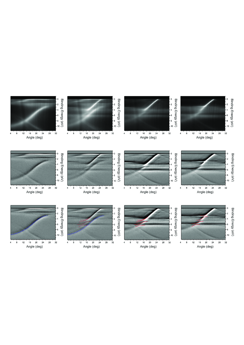
We characterize graphene on Ni(111) intercalated with different amounts of Au by means of scanning tunneling microscopy (STM) and low-energy electron diffraction (LEED): (a,e) Graphene on bare Ni(111) shows a pronounced 3-fold symmetry in STM and a clear pattern in LEED which means that graphene is perfectly in registry to the Ni substrate. (b) Graphene on Ni(111) intercalated with various submonolayer amounts of Au. Underneath of the graphene, the Au forms islands of various dimensions and shapes. STM scans of these islands exhibit the moiré superstucture. This superstructure is attributed to lattice mismatch between Au and Ni. The interatomic distances are in bulk Au 2.88 Å and in bulk Ni 2.48 Å. Since the lattices of graphene and Ni(111) match exactly, it is not surprising that 1 ML Au/Ni(111) also forms a structure at room temperature [Jac95, Ume98]. Underneath the graphene, this structure is rather stable since independently of the exact amount of intercalated Au, these islands always co-exist with areas which resemble cluster superlattices (marked with green arrows). Those areas can be attributed to the formation of an interfacial alloy between Ni and Au under the graphene. Such surface alloy has been observed for Au/Ni(111) after annealing [Ves05]. However, these clusters cover only a minor part of the sample surface and were not found relevant to our results. The fact that we do not observe large areas of alloyed Au under the graphene is understandable: It was shown and demonstrated for CO that the presence of another species reverses the process again (de-alloying) [Ves05]. (c,f) Graphene on Ni intercalated with a full Au monolayer (nominally 1.1 ML) demonstrates in STM and LEED a perfectly periodic moiré pattern. A quantitative analysis is easier for the LEED than for the STM since the superstructure can be evaluated relative to the distance between (0,0) and (1,0) spots without the need for calibration. Our data reveals that the moiré is due to a superstructure. (d,g) Further increase of the Au amount leads to a structure which is less ordered in STM but clearly distinguishable in LEED. When the Au is deposited as a wedge, scanning the sample during LEED shows a clear jump between the and the . (h-k) Corresponding development of the hybridization of graphene with Au states from a wedge-type sample. The phase leads to an additional hybridization around 3 eV binding energy. The SARPES studies of the giant Rashba splitting presented here refer to the phase but the Rashba splitting appears similar in the phase.
References of Supplementary Information
References
[Bih06] G. Bihlmayer, Yu. M. Koroteev, P. M. Echenique, E. V. Chulkov and S. Blügel, The Rashba effect at metallic surfaces, Surf. Sci. 600, 3888 (2006).
[Gio08] G. Giovannetti, P. A. Khomyakov, G. Brocks, V. M. Karpan, J. van den Brink, and P. J. Kelly, Doping graphene with metal contacts, Phys. Rev. Lett. 101, 026803 (2008).
[Jac98] J. Jacobsen, L. P. Nielsen, F. Besenbacher, I. Stensgaard, E. Lægsgaard, T. Ramussen, K. W. Jacobsen, and J. K. Nørskov, Atomic-Scale Determination of Misfit Dislocation Loops at Metal-Metal Interfaces, Phys. Rev. Lett. 75, 489 (1995).
[Nag09] M. Nagano, A. Kodama, T. Shishidou, and T. Oguchi, A first-principles study on the Rashba effect in surface systems, J. Phys.: Condens. Matter 21, 064239 (2009).
[Pet00] L. Petersen and P. Hedeg rd, A simple tight-binding model of spin-orbit splitting of sp-derived surface states, Surf. Sci. 459, 49 (2000).
[Shi08] A. M. Shikin, A. Varykhalov, G. V. Prudnikova, D. Usachov, V. K. Adamchuk, Y. Yamada, J. D. Riley, and O. Rader, Origin of Spin-Orbit Splitting for Monolayers of Au and Ag on W(110) and Mo(110), Phys. Rev. Lett. 100, 057601 (2008).
[Sto91] P. Stoppmanns, B. Heidemann, N. Irmer, N. M ller, B. Vogt, B. Schmiedeskamp, U. Heinzmann, E. Tamura, and R. Feder, Au induced surface state on Pt(111) revealed by spin resolved photoemission with linearly polarized light, Phys. Rev. Lett. 66, 2645 (1991).
[Ton91] A. Ya. Tontegode, Carbon on transition metal surfaces, Prog. Surf. Sci. 38, 201 (1991).
[Ume98] K. Umezawa, S. Nakanishi, and W. M. Gibson, Growth modes depending on the growing temperature in heteroepitaxy: Au/Ni(111), Phys. Rev. B 57, 8842 (1998).
[Var08a] A. Varykhalov, J. Sánchez-Barriga, A. M. Shikin, C. Biswas, E. Vescovo, A. Rybkin, D. Marchenko, and O. Rader, Electronic and magnetic properties of quasifreestanding graphene on Ni, Phys. Rev. Lett. 101, 157601 (2008).
[Var08b] A. Varykhalov, J. Sánchez-Barriga, A. M. Shikin, W. Gudat, W. Eberhardt, and O. Rader, Quantum cavity for spin due to spin-orbit interaction at a metal boundary, Phys. Rev. Lett. 101, 256601 (2008).
[Ves05] E. K. Vestergaard, R. T. Vang, J. Knudsen, T. M. Pedersen, T. An, E. Lægsgaard, I. Stensgaard, B. Hammer, and F. Besenbacher, Adsorbate-Induced Alloy Phase Separation: A Direct View by High-Pressure Scanning Tunneling Microscopy, Phys. Rev. Lett. 95, 126101 (2005).