Supplement: Heat to Electricity Conversion by a Graphene Stripe with Heavy Chiral Fermions
pacs:
84.60.Rb, 73.40.Gk, 73.63.Kv, 44.20.+bI A-I. Non-Equilibrium Thermal Injection
The heat energy flow from the “hot” electrode H with temperature into a much colder heat sinks proceeds along the -stripe with temperature (). The process happens in two stages (i) the thermal injection HRR and (ii) heat/current transfer along the as illustrated by the energy diagrams at the top of Fig. 2b (main text). In the diagram we show the distribution function of “hot” excessive quasiparticles in H where corresponds to the thermally excited excessive electrons while describes the excessive hole thermal excitations [here ]. In stage (i) the temperature difference initializes the non-equilibrium ”thermal injection“ of “hot” electrons and holes from H into the two levels localized inside the recombination region RR. As a result, the upper level becomes inversely populated by the non-equilibrium electrons while the lower level is populated with non-equilibrium holes. The process is described by the quantum kinetic equation Keldysh
| (1) |
In the quasistationary case, one sets which gives
| (2) |
where we have used for the non-equilibrium thermal injection, is the electron-phonon collision term, describes the electron-hole recombination, Rana and accounts for the HCF electron/hole escapes from RR into directions of Ce,h. The corresponding electron distribution functions are approximated as in the H electrode and in the Ce,h shoulders where is the back gate-induced shift of the electron electrochemical potential, is the back gate efficiency, is the Fermi function. Besides, are the effective electron temperatures in the H and Ce,h-adjacent regions. The non-equilibrium distribution function in the RR region then is
| (3) |
where the electron energy broadening is . If using Pd as a metal electrode one typically gets [11] meV for a rough /Pd-interface while meV for a smooth /Pd interface, meV, meV. The temperatures are taken as K, K, and K, the level position meV, which corresponds to the split gate voltage V. The above formulas allows computing the electric and thermal currents. Both types of the currents are inhomogeneous in vicinity of the H and Ce,h electrodes on the corresponding spatial lengths nm and nm. [11] The “hot” conventional electrons coming from H in RR are converted inside RR into the ”heavy” HCF excitations during the short time [11] (in Ref. [11] s, due to the energy level broadening because the tunneling coupling between H and . One finds meV where is the H/RR interface transparency, is the Fermi velocity in H, is the contact barrier thickness). (ii) The second stage consists of the chiral transport, RR, which occurs on the longer timescale s. Then most of the HCF electrons and holes inside RR are captured by the adjacent FETL,R. Simultaneously, minor fractions of HCF electrons and holes annihilate with each other [14] during the time s [typically ]. It sets a requirement to the spatial dimension of RR as m. Since the thermal injection is essentially a non-equilibrium process, the transforming of electron states between the stages (i) and (ii) is incoherent.
Knowing , one computes the electric conductance, , Seebeck coefficient, , and the electronic part of the heat conductance, . The electric current through the H/RR-contact vanishes (formally one gets ) because due to symmetry electron and hole excitations in graphene the electron part of the electric current is compensated by the hole part. For such reasons when computing the conductance for the whole TEG one formally sets the H/RR-contact conductance to zero. The physical meaning of this mathematical trick is that the RR-region is neutral (as the HH-region also is) because number of electrons there is equivalent to the number of holes. For the same reason there is also no finite bias voltage across the H/RR-contact (). The H/RR contact Seebeck coefficient also vanishes since it is . Here where is the bias voltage (which is also equal to zero) and is the temperature difference across the H/RR interface. Besides, due to the opposite electric charge of electrons and holes, one gets . Above we have introduced auxiliary functions where is the driving factor, , is the number of modes, is DOS shown in Fig. 3b (main text), is the -stripe length, is the contact transparency. Unlikely to and , which formally vanish at the H/RR contact, the contact thermal conductance remains essentially finite. A technical complication here is that the electron and hole excitation energies are represented by a non-analytical expression (2). One can overcome that issue by using either of the tricks. The solution of Eq. (2) near the HCF singularity is approximated by an analytical expression as we did at the end of Section II. Another trick is using the model form which gives where is an effective electron temperature difference across the -interface, and .
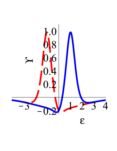
The non-equilibrium injection is characterized by the electron driving factor shown in inset Fig. 4c (main text). The holes are characterized by a very similar factor but it depends on the energy differently: the minimum for holes occurs at the negative energy. We emphasize that both the driving factors, for electrons and holes, give pretty much the same for the electrons and holes. Therefore when computing , one just have to use the electron/hole symmetry and remember that the electron and holes have opposite charge. This approach formally gives no electric current () and no Seebeck effect () through the H/RR interface, while the heat flow due to tunneling electrons and holes is essentially finite. The situation is remarkably different for the electron and hole transport along the G-stripe. Since the electron and hole transports are separated from each other and proceed in opposite directions both, and , i.e., they are essentially finite. The electron/hole heat transfer is shunted by the phonon part of heat flow. However the latter is strongly diminished since the G-stripe is connected in sequence with the multilayer metallic pad with very low heat conductance . A very important consequence of the above properties is that the partial contact conductance and Seebeck coefficient which are immediately related to the metal/graphene interface do not contribute into the and entering for the whole TEG. That happens because the electric current flows only along the graphene stripes, and no electric current occurs between the “hot” electrode and graphene in perpendicular direction. In contrast, the thermal flow occurs between the “hot” metal electrode and graphene, then it splits into the two different directions. The electrons carry the heat to the source electrode while the holes transfer the heat to the drain electrode. The fraction of phonons which penetrate from the “hot” electrode through the multilayered pad into the graphene stripe also splits into the two parts which carry the heat along the graphene stripe in the opposite directions.
There are at least two evident benefits of the tunneling injection from the “hot” electrode into the HCF levels of the graphene stripe. (a) The sharp HCF singularities ensure a very good electric conductance and Seebeck coefficient along the graphene stripe. (b) From the thermal current stand point, the H/RR contact is connected in sequence with the graphene stripe. Next, the thermal conductance of the H/RR contact is much lower than the thermal conductance of the graphene stripe. Therefore the resulting net thermal conductance is considerably diminished. Both the factors, (a) and (b), work toward considerable improving the TEG figure of merit.
Although the contact Seebeck coefficient and the contact electric conductance through the H/RR interface formally vanish (i.e., and , as shown above), the contact thermal conductance remains essentially finite. [6,11] After being thermally injected from H into RR, the electrons and holes are quickly (during time s) converted into the HCF excitations. In the RR region, the non-equilibrium HCF electrons and holes populate the levels inversely: the upper level is populated by excessive HCF electrons while the lower level by the excessive HCF holes.
In the configuration shown in Fig. 2 (main text), the holes ballistically propagate from RR toward Ch while the electrons in the left -section proceed from RR toward Ce. Thus, the latter stage implies a chiral transmission of the excessive non-equilibrium HCF electrons from the upper level localized in RR into the upper level located in the uncovered -section adjacent to Ce (see the diagram at the top of Fig. 2b, main text) where , is the localized level width. Simultaneously, the excessive holes are transmitted from the lower level in RR into the lower level localized near Ch. In this way, the full thermal flow from H to RR is eventually split between the Ch and Ce sections of the graphene stripe . In the uncovered -section, broadening of the HCF level originates from coupling of the HCF states to the phonons. It yields (typically s at K). In the RR section, there is an additional coupling [11] to the electron states in H which gives .
Along the -stripe, the TEG parameters , , and are determined purely by the electron and hole transport. The underlying physical mechanism is the chiral transmission of the HCF electrons and holes from the neutral RR section to the voltage p- and n-doped -sections. In the same approximation, one evaluates the electric conductance of FETL,R along the -stripe between the RR and Ce,h as
| (4) | |||||
where is shown in Fig. 4d (main text). Analogously, one finds Seebeck coefficient along the -stripe and . The last result indicates that Seebeck coefficient could be huge while the electron/hole part of the thermal conductance along the stripe is typically low. The phonon part of the heat energy flow is where W/K at K while the number of phonon modes also depends on the temperature and the stripe geometry. The electron/hole heat energy flow is
| (5) | |||||
where we have used , , , and we have defined the factor . Because
| (6) |
can be big, , one might achieve huge values of . Typically , therefore the -TEG net “phonon” heat conductance Cahill is , which can be comparable to the contact electron heat conductance . It means that only the contact electron/hole and phonon heat conductances actually contribute into . Summarizing the above estimates one arrives at .
I.1 A-II. Blocking the phonon flow by multilayered electrodes.
I.1.1 Electric/heat conductance valve
A general scenario for improvement the figure of merit implies increasing the Seebeck coefficient and electric conductance on one hand while reducing the heat conductance on the other hand. A considerable raise of S and G is achieved by implementing the quantized state resonances. The reducing of while preserving and is accomplished when implementing of metallic multilayers with the layer thickness randomly changed between nm. The random layer thickness change is introduced to eliminate resonance transmission of phonons. Thus the phonon flow across the multilayer is decimated due to the low transmission probability . However the contribution of phonons to the heat transfer might exceed the contribution due to the electrons and holes. The multilayer actually acts like a filter for the two components of microscopic heat transport.
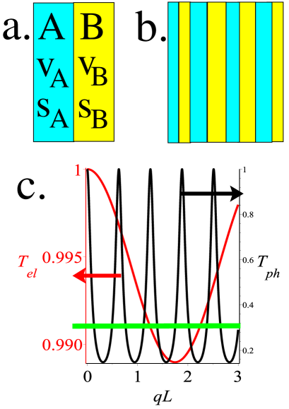
The heat flow filtering mechanism is understood within a simple analytical model. The multilayer represents a sequence of bilayers shown in Fig. 2a (main text) where metallic layers A and B are characterized by different Fermi () and sound () velocities. The phonon heat conductance through the multilayer is obtained from the Landauer formula. [27,28] One writes
| (7) |
where and are the temperatures and the Bose-Einstein distribution functions in the “hot” and “cold” ends. The phonon transmission probability is obtained by the mode matching method. Ando2 If the temperature gradient across the junction is small, , and the junction is ideally transparent for phonons, , is quantized Yama as where is the number of acoustic modes. For m and nm one roughly gets W/(mK).
Electron transport through the metallic multilayer is determined by the corresponding electrons () and phonons () transmission probabilities. We compute and in terms of the S-matrix method. Datta The electron S-matrix of the whole ABAB multilayer is composed of elementary blocks ABA. Here we assume that there are no interface A/B-barriers separating the A and B layers. The electron (hole) transmission () and reflection () coefficients which are the SABA matrix elements are obtained from the A/B-interface boundary conditions as (see, e.g., Ref. [4])
| (8) |
where the denominator is , and are the electron wavevectors in A and B. Since the main contribution to and comes from the electron states near the Fermi level, one may use the linear dispersion law . Since the electron energy is conserved during the interlayer transmission, it gives or . This allows rewring of Eq. (8) simply as
| (9) |
where now and . The corresponding phonon transmission and reflection coefficients are derived in a similar way.
A very interesting consequence of the above formula takes place when for electrons while simultaneously for phonons. Such situation takes place, e.g., when one of the metals in the elementary bilayer is lead (i.e., A=Pb) while another metal is aluminium (B=Al). The Fermi velocities for the lead and aluminium are very close ( m/s and m/s respectively) while the sound velocities in the two metals are quite different (i.e., m/s and m/s). This gives a big difference between the two ratios on one hand while on the other hand. The whole ABAAB multilayer is then composed as a sequence of bilayers with randomly changing thickness. As is evident from Fig. 2 c, the electron transmission probability through the whole metallic multilayer shown in Figs. 2c (main text), 2 a,b is nearly ideal, while the phonon transport is practically blocked since .
Since the lattice constants of the two metals A and B differ, there is a lattice strain immediately at the layer’s A/B-interfaces. However, the strained region involves just a few atomic layers at the Pb/Al or Pb/Sn interfaces. Therefore the strain affects just on a tiny fraction of the whole multilayer’s volume. Contribution of that strained region into the electron and phonon transport across the metallic multilayer is negligible if the length of the strained region in lateral direction is much shorter than the metallic layer thickness or/and the electron and phonon mean free paths. Similar metallic multilayers had been widely used in the superconducting junction technology and it is well known the interface strains do not impact the lateral electron transport. That happens because it acts just like a scatterer which size is less than 1 nm, i.e., it is much narrower than the phonon’s wave length of interest which exceeds 10 nm for 300 K. The strained region is too narrow to change the electron band structure on the local scale nm. The local short scale lattice deformation nm is also unable to generate an electrostatic potential barrier for the electrons propagating in the lateral direction.
The difference in transmission probabilities of the electrons and phonons through the metallic multilayer can be exploited to filter the heat transport components: The electrons and holes propagate through the metallic multilayer almost free while the phonon transport is considerably reduced.
The above simple analytical model is supported here by more rigorous numeric calculations. The filter pads are introduced to separate the -section both from the external electrodes and from the substrate thermally, but not electrically. We consider two different types of the heat/electric current valve pads. One design involves metallic multi-layers Pb/Al with the layer thickness nm. Another method is to depositing of pads made of SrHfO3 and/or SrRuO3. The layered materials have an appreciable electric conductance while their thermal conductance along the c-axis is remarkably low. Keawprak ; Maekawa Planting of the H/RR pad between the metallic electrodes and graphene stripe would reduce the effective significantly, because the phonons which provide between the hot and cold ends are eliminated from the thermoelectric path. Then the net heat conductance which involves the path HOT RR Ce,h COLD will be considerably diminished. Thus placing of the H/RR pad with a sufficient number of nanolayers allows to decimating of the phonon part the whole thermal conductance . The optimal -TEG geometry is also determined by the electric and thermal transfer lengths which are estimated [6,11] correspondingly as nm and nm.
I.2 A-III. Numeric simulations.
The phonon part of the thermal transport through the TEG had been examined as follows. We describe the non-equilibrium heat flow through the -stripe in presence of multiple scattering on lattice defects, boundaries, and electrons. A finite temperature difference between the opposite ends of each -stripe induces the thermal flow given as a sum of contributions of the individual phononic subbands. The phonon density of states related to the phonon subband is mismatched in adjacent layers of the H electrode sketched in Fig. 2c (main text). Inside the -stripe, the phonon distribution function is non-equilibrium which means that deviates from the Bose-Einstein distribution in the hot (H) and cold (C) ends. For a ”clean” graphene stripe, the phonon mean free path exceeds the -stripe length . Therefore the non-equilibrium effect does not influence the final results. The equilibrium phonon distribution at the -stripe ends is established due to a free phonon diffusion into the bulk of attached metallic contacts and dielectric substrate. The thermal conductance of the -stripe had been computed by using the phonon density of states preliminary obtained for each phonon subband .
The thermoelectric characteristics are found by solving the Dirac equation for chiral fermions in graphene (see above). The analytical model is verified by numeric calculations based on the density functional theory. Fertig The electron and phonon excitation spectra are obtained considering influence of the inelastic electron-phonon and elastic electron-impurity scatterings. They are taken into account along with processes of the electron tunneling through the interface barriers. The electron-impurity and electron-phonon scatterings are included within the Keldysh-Green function technique [25] which allows deriving of the quantum kinetic equations.
I.3 A-IV. Transparency of the H/RR interface.
The thermal injection efficiency is directly related to transparency of the H/RR interface. The interface barriers which contribute into originate from the difference of the workfunctions in the metallic H electrode and the graphene -stripe right beneath of it [11,15]. The heat-conducting Ch, H, and Ce electrodes are deposited at the top of the -stripe, as schematically shown in Fig. 2 (main text). Another factor is change in the number of conducting channels when electrons and holes tunnel from the 3D metallic H electrode into the 2D graphene -stripe. [21] Conversion of the regular electrons and holes into the HCF excitations also contributes to . Thus, for the -TEG, depends on the 3D/2D conversion efficiency and on the spatial distribution of charge carriers near the H/RR interface. The contact thermal conductance problem and its solution are illustrated in Fig. 4 (main text). In Fig. 4a (main text) we plot the transmission probability as a function of the electron energy for the conventional electrons penetrating a non-chiral potential barrier (curve 1), and the quantum well (curve 2). Curve 3 shows for the non-chiral heavy fermions transmitting via a potential well. One can see that is strongly suppressed in the latter case. For such a reason, the contact conductance for conventional ”heavy“ fermions is low. Quite a different behavior takes place if instead of the conventional ”heavy“ electrons there are the ”heavy“ chiral (HCF) particles as is evident from Fig. 4b (main text). In Fig. 4b (main text) we compare for the conventional chiral fermions penetrating the chiral barrier (curves 1 and 3) with the same characteristics for HCF particles (curves 2 and 4). One can see that is fairly good for both types of the chiral particles if the incidence angle is small, i.e., (curves 1 and 2). For bigger incidence angles, i.e., (curves 3 and 4), for the HCF particles becomes suppressed (curve 4). The electron thermal conductance of -TEG is determined by . The dominant contribution into comes at the low angles , therefore using of the HCF particles helps to maintaining of at a decent level.
I.4 A-V. Graphene TEG parameters
When evaluating the figure of merit and the electric power density of the graphene TEG we admit the following parameters. The in-plane thermal conductivity of graphene Balandin-1 ; Seol is about 1000 W/(mK) and is determined by acoustic phonons. This is consistent with Refs. [5,6], where for graphene layer thickness nm (which corresponds to layers), the in-plane thermal conductance is MW/(mK). Anisotropy of the thermal conductivity (in plane)/(out plane) is about 1000 for the graphene/metal contact area which gives the cross-plane thermal conductance MW/(mK). At K for Au/Ti/n-lG/SiO2 multilayer one gets [5,6] the thermal conductance as MW/(mK) while for Au/Ti/SiO2 multilayer one obtains instead MW/(mK). At the same time, the thermal conductance for the 1-lG/SiO2 interface (1-lG stands for the one-layer graphene) is MW/(mK). The electron heat conductance has typically 3-4 orders of magnitude lower values than the phonon which gives . Therefore heat transfers along the graphene plane and across the metal/graphene interface are carried predominantly by phonons.
The in-plane sound velocity of graphene is m/s. The Gaussian broadening to model the random disorder potential in the channel is used with meV, corresponding to an experimental (minimum sheet carrier concentration) of cm-2.
There is a controversy in the literature concerning the electron-electron collision time . Some authors regard at room temperatures as short as s which gives the mean free path between the electron-electron scattering as cm = 1 nm. According to the experiment reported in Ref. Bolotin , an actual mean electron free path in nanotubes at K is at least three orders of magnitude longer and might far exceed 1 m which gives the lower bond for s.
Broadening of the electron levels due to coupling of electron states in adjacent regions we model here following Refs. Perebei ; Giovan ; Nemec-1 ; Nemec-2 . According to Perebei ; Giovan ; Nemec-1 ; Nemec-2 , we use the broadening caused by the /Pd-interface ramdomness as meV, whereas meV for an ideal /Pd interface, meV, and meV. The temperatures are obtained self-consistently using the aforementioned values of the thermal conductance. Then we get meV and meV. In addition to the inhomogeneous broadening, graphene states under the metal have a homogeneous (lifetime) broadening due to coupling to the metal. Following to Ref. Perebei , we model the total broadening by a Voigt function , which is a convolution of a Gaussian of width and a Lorentzian of width (which is typically eV), and a cutoff energy of 1 eV, which is the typical bandwidth of d-bands in transition metals. The random potential disorder is expected to be much larger under the polycrystalline metal than in the channel. For a variation of the metal–graphene distance of 2 Å (from 3 Å to 5 Å), a 0.9 eV change in potential has been calculated.
We also set the level position as meV which corresponds to the same value of the split gate voltage. The HCF peak width is evaluated from know experimental data Bolotin concerning the electron mean free path which in ”clean” anealed graphene could be as much as m which gives meV. That corresponds to and .
The quantum of thermal conductance at K is while at K it is W/K. The electric power generated by a single -TEG is evaluated as W mW where we used V, is the quantum conductance and we have introduced a large dimensionless factor
| (10) |
where we used the ratio of HCF and free electron mass as while the ratio of the temperature differences is obtained as . The length of a single -TEG element is m. The -stripe width is nm. The period of -stripe array in the y-direction is set as nm. Then the TEG device by size 1 cm1 cm contains -TEG elements which theoretically might generate the electric power 10 1 mW = 1 MW.
References
- (1) A. I. Persson, Y. Kan Koh, D. G. Cahill, L. Samuelson, and H. Linke, Nano Lett., 9, 4484 (2009).
- (2) L. Brey, H. A. Fertig, Phys. Rev. B75, 125434 (2007).
- (3) F. Xia, V. Perebeinos, Y.-m. Lin, Y. Wu, and Ph. Avouris, Nature Nanotechnology, 6, 179 (2011).
- (4) F. Rana, Phys. Rev. B76, 155431 (2007).
- (5) G. Giovannetti, P. A. Khomyakov, G. Brocks, V. M. Karpan, J. van den Brink,and P. J. Kelly, Phys. Rev. Lett., 101, 026803 (2008).
- (6) S. Datta, Electronic Transport in Mesoscopic Systems (Cambridge Univ. Press, Cambridge, 1997).
- (7) T. Ando, J. Phys. Soc. Jpn 74, 777 (2005).
- (8) N. Keawprak, R. Tu, and T. Goto, In: Materials Science and Engineering: B 161, 71 (2009).
- (9) T. Maekawa, K. Kurosaki, H. Muta, M. Uno, and S. Yamanaka, J. Alloys Compd. 387, 56 (2005).
- (10) L. V. Keldysh, [Zh. Eksp. Teor. Fiz. 47, 1515 (1964)] Sov. Phys. JETP 20, 1018 (1965).
- (11) T. Yamamoto and K. Watanabe, Phys. Rev. Lett. 96, 255503 (2006).
- (12) L. G. C. Rego and G. Kirczenov, Phys. Rev. Lett. 81, 232 (1998).
- (13) T. Ando, Phys. Rev. B 44, 8017 (1991).
- (14) A. A. Balandin, S. Ghosh, W. Bao, I. Calizo, D. Teweldebrhan, F. Miao, & C. N. Lau, 8, 902 (2008).
- (15) J. H. Seol, I. Jo, A. L. Moore, L. Lindsay, Z. H. Aitken, M. T. Pettes, X. Li, Z. Yao, R. Huang, D. Broido, N. Mongo, R. S. Ruoff, & L. Shi, Science, 328, 213 (2010).
- (16) K. I. Bolotin, K. J. Sikes, Z. Jiang, G. Fudenberg, J. Hone, P. Kim, & H. L. Stormer, Sol. State Comm. 146, 351 (2008).
- (17) N. Nemec, D. Tomanek, & G. Cuniberti, Phys. Rev. Lett. 96, 076802 (2006).
- (18) N. Nemec, D. Tomanek, & G. Cuniberti, Phys. Rev. B 77, 125420 (2008).