New layered fluorosulfide SrFBiS2
Abstract
We have synthesized a new layered BiS2-based compound SrFBiS2. This compound has similar structure to BiS2. It is built up by stacking up SrF layers and NaCl-type BiS2 layers alternatively along the c axis. Electric transport measurement indicates that SrFBiS2 is a semiconductor. Thermal transport measurement shows that SrFBiS2 has a small thermal conductivity and large Seebeck coefficient. First principle calculations are in agreement with experimental results and show that SrFBiS2 is very similar to LaOBiS2 which becomes superconductor with F doping. Therefore, SrFBiS2 may be a parent compound of new superconductors.
I Introduction
Low-dimensional superconductors with layered structure have been extensively studied and still attract much interest due to their exotic superconducting properties and mechanism when compared to conventional BCS superconductors. The examples include high cuprates,Bednorz Sr2RuO4,Maeno NaxCoOH2O,Takada and iron-based superconductors.Kamihara The discovery of LnOFePn (Ln = rare earth elements, Pn = P, As) in particular revitalises the study of layered compounds with mixed anions, paving a way to materials with novel physical properties. For example, Ln2O2TM2OCh2 (TM = transition metals, Ch = S, Se) show strong electron-electron interactions and Mott insulating state on the two dimensional (2D) frustrated antiferromagnetic (AFM) checkerboard spin-lattice.Mayer -Free Very recently, bulk superconductivity was found in BiS2-type layered compounds with mixed anions: Bi4O4S3 and Ln(O,F)BiS2.Mizuguchi1 -Demura Experimental and theoretical studies indicate that these materials exhibit multiband behaviors with dominant electron carriers originating from the Bi 6 and 6 bands in the normal state.Usui -Tan On the other hand, compounds with mixed anions exhibit remarkable flexibility of structure. Different two-dimensional (2D) building blocks, such as [LnO]+, [AEF]+ (AE = Ca, Sr, Ba), [Ti2OPn2]2-, [FePn]-, and [TM2OCh2]2-, can sometimes be integrated to form new materials.Kamihara ,Matsuishi -Liu2 Individual building blocks often keep their structural and electronic properties after being combined together.Kabbour
In this work, we report the discovery of a new BiS2-based layered compound SrFBiS2. It contains NaCl-type BiS2 layer and shows semiconducting behavior with relatively large thermopower. Theoretical calculation indicates that this compound is very similar to LnOBiS2.
II Experiment
II.1 Synthesis.
SrFBiS2 polycrystals were synthesized by a two-step solids state reaction. First, Bi2S3 was prereacted by reacting Bi needles (purity 99.99%, Alfa Aesar) with sulfur flakes (purity 99.99%, Aldrich) in an evacuated quartz tube at 600 for 10 h. Then Bi2S3 was mixed with stoichiometric SrF2 (purity 99%, Alfa Aesar) and SrS (purity 99.9%, Alfa Aesar) and intimately ground together using an agate pestle and mortar. The ground powder was pressed into 10 mm diameter pellets. We used a maximum pressure of 5 tons. The pressed pellet was loaded in an alumina crucible and then sealed in quartz tubes with Ar under the pressure of 0.15 atmosphere. The quartz tubes were heated up to 600 in 10 h and kept at 600 for another 10 h.
II.2 Structure and Composition Analysis.
Phase identity and purity were confirmed by powder X-ray diffraction carried out by a Rigaku Miniflex X-ray machine with Cu Kα radiation ( = 1.5418 Å). Structural refinement of powder SrFBiS2 sample was carried out by using Rietica software.Hunter Synchrotron X-ray experiment was conducted at 300 K on X17A beamline of the National Synchrotron Light Source (NSLS) at Brookhaven National Laboratory (BNL). The setup utilized X-ray beam 0.5 mm 0.5 mm in size and = 0.1839 Å ( = 67.4959 keV), conditioned by two-axis focusing with one-bounce sagittally-bent Laue crystal monochromator, and Perkin-Elmer image plate detector mounted perpendicular to the primary beam path. Finely pulverized sample packed in cylindrical polyimide capillary 1mm in diameter was placed 204 mm away from the detector. Multiple scans were performed to a total exposure time of 120 . The 2D diffraction data were integrated and converted to intensity versus 2 using the software FIT2D.Hammersley The intensity data were corrected and normalized and converted to atomic pair distribution function (PDF), , using the program PDFgetX2.Qiu The average stoichiometry of SrFBiS2 polycrystal was determined by examination of multiple points using an energy-dispersive x-ray spectroscopy (EDX) in a JEOL JSM-6500 scanning electron microscope.
II.3 Electrical and Thermal Transport Measurements.
The sample pellets were cut into rectangular bar and the surface is polished by sandpaper. Thin Pt wires were attached using silver epoxy for four probe resistivity measurements. Electrical and thermal transport measurements were carried out in Quantum Design Physical Property Measurement System (PPMS-9).
II.4 Band Structure Calculations.
First principle electronic structure calculation were performed using experimental crystallographic parameters within the full-potential linearized augmented plane wave (LAPW) method wien2k1 implemented in WIEN2k package.wien2k2 The general gradient approximation (GGA) of Perdew et al.,gga was used for exchange-correlation potential. The LAPW sphere radius were set to 2.5 Bohr for all atoms, and the converged basis corresponding to with additional local orbital were used where is the minimum LAPW sphere radius and is the plane wave cutoff.
III Results and Discussion
III.1 Structure and Compostion.
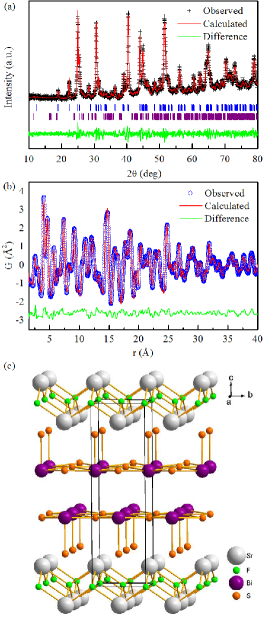
Fig. 1(a) shows the powder XRD pattern of SrFBiS2 measured by Rigaku Miniflex. Almost all of reflections can be indexed using the P4/nmm space group. The unidentified peaks belong to the second phase of Bi2S3. Using two-phase Le Bail fitting, the refined lattice parameters of SrFBiS2 are = 4.084(2) Å and = 13.798(2) Å. When compared to LaOBiS2, the a-axial lattice parameter is larger and the c-axial one is slightly smaller.Mizuguchi2 The PDF structural analysis was carried out using the program PDFgui.Farrow The SrFBiS2 data are explained well within the model having P4/nmm symmetry with = 4.079(2) Å and = 13.814(5) Å( = 0.138, =0.024). It is consistent with the fitting results obtained from Miniflex. The final fit is shown in Fig. 1(b), and the results are summarized in Table 1. In addition to the principal phase, the sample is found to have 16(1) wt% of Bi2S3 impurity with Pnma symmetry, which is also observed in Fig. 1(a). Structure of SrFBiS2 is similar to LaOBiS2, which is built up by stacking the rock-salt-type BiS2 layer and fluorite-type SrF layer alternatively along the c axis as shown Fig. 1(c). The EDX spectrum of polycrystal confirms the presence of Sr, F, Bi, and S. The average atomic ratios determined from EDX are Sr : F : Bi : S = 1.00(4) : 1.00(9) : 1.03(5) : 1.88(4) when setting the content of Sr as 1. It confirms the formula of obtained compound is SrFBiS2.

| Chemical Formula | SrFBiS2 | ||||
| Formula Mass (g/mol) | 379.73 | ||||
| Crystal System | Tetragonal | ||||
| Space Group | P4/nmm (No. 129) | ||||
| (Å) | 4.079(2) | ||||
| (Å) | 13.814(5) | ||||
| (Å3) | 229.8(3) | ||||
| Z | 2 | ||||
| Density (g/cm3) | 5.51 | ||||
| Atom | site | x | y | z | (Å2)a |
| Sr | 2c | 1/4 | 1/4 | 0.1025(2) | 0.0069(4) |
| F | 2a | 3/4 | 1/4 | 0 | 0.033(2) |
| Bi | 2c | 1/4 | 1/4 | 0.6286(5) | 0.0183(3) |
| S1 | 2c | 1/4 | 1/4 | 0.379(3) | 0.060(2) |
| S2 | 2c | 1/4 | 1/4 | 0.811(2) | 0.019(1) |
| a is defined as one-third of the orthogonalized tensor. | |||||

III.2 Electrical Properties.
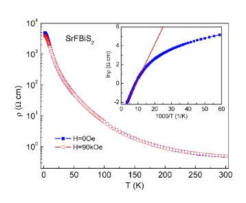
As shown in Fig. 2, the resistivity of SrFBiS2 polycrystalline shows a semiconducting behavior in the measured temperature region (1.9-300 K). It should be noted that Bi2S3 polycrystal shows metallic behavior becasue of sulfur deficiency.Chen The impurity may have some minor influence on the absolute value of resistivity, but the semiconducting behavior should be intrinsic. Neglecting the grain boundary contribution, the room-temperature resistivity K is about 0.5 cm. Using the thermal activation model ( is a prefactor, thermal activated energy and the Boltzmann’s constant) to fit the at high temperature (75 K - 300 K) (inset of Fig. 2), we obtain = 31.8(3) meV. The semiconductor behavior is consistent with theoretical calculation result shown below. On the other hand, theoretical calculations have indicated that undoped LaOBiS2 is also a semiconductor, which is partially consistent with the experimental result.Usui ,Awana Transport measurement indicates that LaOBiS2 shows semiconducting behavior at 200 K, but exhibit an upturn of resistivity at higher temperature. The origin of the upturn is unclear. Therefore, the replacement of LaO by SrF should not change the band structure and thus physical properties too much, especially at low temperature, similar to the relation between SrFFeAs and LaOFeAs.Han ,Dong The slight differences between LaOBiS2 and SrFBiS2, such as larger a-axial and smaller c-axial lattice parameters, could result in changing of physical properties at higher temperature. Note that the semiconducting in LaOBiS2 and SrFBiS2 are different from those in parent compounds of iron pnictide superconductors. The latter show metallic behaviors at high temperature and semiconducting-like upturn in resistivity curve related to the spin density wave (SDW) transition. There is no significant magnetoresistance in SrFBiS2 up to 90 kOe magnetic field.

III.3 Thermal Transport Properties.
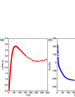
The temperature dependences of the thermal conductivity and thermoelectric power (TEP) for SrFBiS2 in zero field between 2 and 350 K are shown in Fig. 3. The electronic thermal conductivity estimated from the Wiedemann-Franz law using a value for the Lorenz number of 2.4410-8 W /K2 was less than 510-6 of . Therefore, lattice thermal conductivity dominates which exhibits a peak at around 60 K (Fig. 1(a)). The peak in commonly arises since different phonon scattering processes usually dominate in different temperature ranges. Umklapp scattering dominates at high temperatures, while boundary and point-defect scattering dominate at low and intermediate temperatures, respectively.Yang On the other hand, the of SrFBiS2 shows similar behavior to Bi4O4S3 but with different peak position and absolute value.Tan For TEP of SrFBiS2, there is a reversal in sign at about 11 K, i.e, hole-like carrier changes into electron-like carrier which is dominant at room temperature. According to two band model, .Tan If we assume that and are temperature independent, it suggests that electron and hole conductivities change dramatically with temperature: at low temperature, whereas above 11 K. Hole-like carrier may originate from defect induced p-type doping. With increasing temperature, electron-like carrier due to intrinsic band excitation increase significantly, finally leading to and a sign change in . Similar behavior was observed in LaOZnP and p-type Si.Kayanuma ; Seeger Even though the in SrFBiS2 is significant and not much smaller than in classics thermoelectric materials, Row its low electrical conductivity makes its figure of merit ZT (ZT = S2T/) extremely small.

III.4 Electronic Structure.
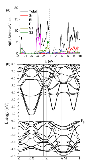
First principle calculations (Fig. 4) confirm that SrFBiS2 is a semiconductor with a direct band gap of 0.8 eV located at point. This is similar to LaOBiS2 where the energy gap was found to be 0.82 eV.Wan The calculation confirms the results of transport measurement. Similar to LaOBiS2,Usui ,Wan both S and Bi states are located around the Fermi level (-2.0 to 2.0 eV) in SrFBiS2. Thus there is a strong hybridization between S and Bi states. The absence of dispersion along line suggests quasi two dimensional character of the band structure in SrFBiS2 (Fig. 4(b)). In LaOBiS2, F doping results in metallic states and superconductivity at low temperature. Main influence of F substitution is a carrier doping that shifts the Fermi level and has only minor effect on the lowest conduction band. Due to similarity between SrFBiS2 and LaOBiS2, new superconductors could be obtained by chemical substitution.
IV Conclusion
In summary, we report a discovery of a new layered fluorosulfide SrFBiS2. It contains NaCl-type BiS2 layer similar to Bi4O4S3 and Ln(O,F)BiS2 superconductors. SrFBiS2 polycrystals shows semiconducting behavior between 2 K and 300 K. We observe rather small thermal conductivity and large TEP with sign reversal at low temperature. Theoretical calculation confirms the semiconducting behavior and indicates similar DOS and band structure to undoped LaOBiS2. Because of the similarity between SrFBiS2 and the parent compound of BiS2-based superconductors, it is of interest to investigate the doping effects on physical properties of SrFBiS2. It could pave a way to new members in this emerging family of BiS2-based superconductors.
V Acknowledgements
We thank John Warren for help with SEM measurements. Work at Brookhaven is supported by the U.S. DOE under Contract No. DE-AC02-98CH10886 and in part by the Center for Emergent Superconductivity, an Energy Frontier Research Center funded by the U.S. DOE, Office for Basic Energy Science (H. L. and C. P.). This work benefited from usage of X17A beamline of the National Synchrotron Light Source at Brookhaven National Laboratory. We gratefully acknowledge Zhong Zhong and Jonathan Hanson for their help with the X17A experiment setup.
References
- (1) J. G. Bednorz and K. A. Muller, Z. Physik B 64, 189 (1986).
- (2) Y. Maeno, H. Hashimoto, K. Yoshida, S. Nishizaki, T. Fujita, J. G. Bednorz, and F. Lichtenberg, Nature 372, 532 (1994).
- (3) K. Takada, H. Sakurai, E. Takayama-Muromachi, F. Izumi, R. A. Dilanian, and T. Sasaki, Nature 422, 53 (2003).
- (4) Y. Kamihara, T. Watanabe, M. Hirano, and H. Hosono, J. Am. Chem. Soc. 130, 3296 (2008).
- (5) J. M. Mayer, L. F. Schneemeyer, T. Siegrist, J. V. Waszczak and B. Van Dover, Angew. Chem., Int. Ed. Engl. 31, 1645 (1992).
- (6) C. Wang, M. Q. Tan, C. M. Feng, Z. F. Ma, S. Jiang, Z. A. Xu, G. H. Cao, K. Matsubayashi and Y. Uwatoko, J. Am. Chem. Soc. 132, 7069 (2010).
- (7) J.-X. Zhu, R. Yu, H. Wang, L. L. Zhao, M. D. Jones, J. Dai, E. Abrahams, E. Morosan, M. Fang and Q. Si, Phys. Rev. Lett. 104, 216405 (2010).
- (8) N. Ni, E. Climent-Pascual, S. Jia, Q. Huang and R. J. Cava, Phys. Rev. B 82, 214419 (2010).
- (9) D. G. Free, N. D. Withers, P. J. Hickey and J. O. Evans, Chem. Mater. 23, 1625 (2011).
- (10) Y. Mizuguchi, H. Fujihisa, Y. Gotoh, K. Suzuki, H. Usui, K. Kuroki, S. Demura, Y. Takano, H. Izawa, O. Miura, Phys. Rev. B 86, 220510(R) (2012).
- (11) Y. Mizuguchi, S. Demura, K. Deguchi, Y. Takano, H. Fujihisa, Y. Gotoh, H. Izawa, O. Miura, J. Phys. Soc. Jpn. 81, 114725 (2012).
- (12) S. Demura, Y. Mizuguchi, K. Deguchi, H. Okazaki, H. Hara, T. Watanabe, S. J. Denholme, M. Fujioka, T. Ozaki, H. Fujihisa, Y. Gotoh, O. Miura, T. Yamaguchi, H. Takeya, and Y. Takano, arXiv 1207.5248.
- (13) H. Usui, K. Suzuki, K. Kuroki, Phys. Rev. B 86, 220501(R) (2012).
- (14) S. Li, H. Yang, J. Tao, X. Ding, and H.-H. Wen, arXiv 1207.4955.
- (15) S. K. Singh, A. Kumar, B. Gahtori, Shruti, G. Sharma, S. Patnaik, and V. P. S. Awana, J. Am. Chem. Soc 134, 16504 (2012).
- (16) S. G. Tan, L. J. Li, Y. Liu, P. Tong, B. C. Zhao, W. J. Lu, Y. P. Sun, Physica C 483, 94 (2012).
- (17) S. Matsuishi, Y. Inoue, T. Nomura, H. Yanagi, M. Hirano, and H. Hosono, J. Am. Chem. Soc. 130, 14428 (2008).
- (18) F. Han, X. Y. Zhu, G. Mu, P. Cheng, and H.-H. Wen, Phys. Rev. B 78, 180503 (2008).
- (19) H. Kabbour, L. Cario, and F. Boucher, J. Mater. Chem. 15, 3525 (2005).
- (20) R. H. Liu, J. S. Zhang, P. Cheng, X. G. Luo, J. J. Ying, Y. J. Yan, M. Zhang, A. F. Wang, Z. J. Xiang, G. J. Ye and X. H. Chen, Phys. Rev. B 83, 174450 (2011).
- (21) R. H. Liu, Y. A. Song, Q. J. Li, J. J. Ying, Y. J. Yan, Y. He, and X. H. Chen, Chem. Mater. 22, 1503 (2010).
- (22) Hunter B. (1998) ”Rietica - A visual Rietveld program”, International Union of Crystallography Commission on Powder Diffraction Newsletter No. 20, (Summer) http://www.rietica.org
- (23) A. P. Hammersley, S.O. Svenson, M. Hanfland, and D. Hauserman, High Press. Res. 14, 235 (1996).
- (24) X. Qiu, J. W. Thompson, and S. J. L. Billinge, J. Appl. Crystallogr. 37, 678 (2004).
- (25) M. Weinert, E. Wimmer, and A. J. Freeman, Phys. Rev. B 26, 4571 (1982).
- (26) P. Blaha, K. Schwarz, G. K. H. Madsen, D. Kvasnicka and J. Luitz, WIEN2k, An Augmented Plane Wave + Local Orbitals Program for Calculating Crystal Properties (Karlheinz Schwarz, Techn. Universitat Wien, Austria), 2001. ISBN 3-9501031-1-2
- (27) J. P. Perdew, K. Burke and M. Ernzerhof, Phys. Rev. Lett. 77, 3865 (1996).
- (28) C. L. Farrow, P. Juhas, J. W. Liu, D. Bryndin, E. S. Bozin, J. Bloch, Th. Proffen, and S. J. L. Billinge, J. Phys.: Condens. Mater. 19, 335219 (2007).
- (29) B. Chen, C. Uher, L. Iordanidis, and M. G. Kanatzidis, Chem. Mater. 9, 1655 (1997).
- (30) V. P. S. Awana, A. Kumar, R. Jha, S. Kumar, J. Kumar, and A. Pal, arXiv 1207.6845.
- (31) J. Dong, H. J. Zhang, G. Xu, Z. Li, G. Li, W. Z. Hu, D. Wu, G. F. Chen, X. Dai, J. L. Luo, Z. Fang, and N. L. Wang, EPL 83, 27006 (2008).
- (32) J. Yang, D. T. Morelli, G. P. Meisner, W. Chen, J. S. Dyck, and C. Uher, Phys. Rev. B 65, 094115 (2002).
- (33) K. Seeger, in Semiconductor Physics: An Introduction, Springer-Verlag, Berlin (2004).
- (34) K. Kayanuma, H. Hiramatsu, M. Hirano, R. Kawamura, H. Yanagi, T. Kamiya, and H. Hosono, Phys. Rev. B 76, 195325 (2007).
- (35) D. M. Rowe, in Thermoelectrics Handbook: Macro to Nano, Taylor & Francis, London (2006).
- (36) X. Wan, H.-C. Ding, S. Y. Savrasov, and C.-G. Duan, arXiv 1208.1807.