Disorder effects on resonant tunneling transport in GaAs/(Ga,Mn)As heterostructures
Abstract
Recent experiments on resonant tunneling structures comprising (Ga,Mn)As quantum wells [Ohya et al., Nature Physics 7, 342 (2011)] have evoked a strong debate regarding their interpretation as resonant tunneling features and the near absences of ferromagnetic order observed in these structures. Here, we present a related theoretical study of a GaAs/(Ga,Mn)As double barrier structure based on a Green’s function approach, studying the self-consistent interplay between ferromagnetic order, structural defects (disorder), and the hole tunnel current under conditions similar to those in experiment. We show that disorder has a strong influence on the current-voltage characteristics in efficiently reducing or even washing out negative differential conductance, offering an explanation for the experimental results. We find that for the Be lead doping levels used in experiment the resulting spin density polarization in the quantum well is too small to produce a sizable exchange splitting.
pacs:
85.75.Mm, 73.23.Ad, 73.63.-b, 72.25.DcI Introduction
Dilute magnetic semiconductors (DMS) are produced by doping of semiconductors with transition metal elements, which provide local magnetic moments arising from open electronic or shells.Jungwirth et al. (2006); Burch et al. (2008) Bulk Ga1-xMnxAs may be regarded as the prototype: Mn residing on the Ga site (MnGa) donates a hole, associated with valence band p-orbitals, and provides a local magnetic moment associated with partly filled Mn d-orbitals. MnGa is a moderately deep acceptor with the energy levels lying about 100 meV above the valence band edge.Schneider et al. (1987) By increasing the Mn density the acceptor levels become more and more broadened, developing into an impurity band which allows hole propagation and, for sufficiently high doping level, is believed to merge with the valence band.Jungwirth et al. (2007) At the same time, Mn more and more takes unwanted lattice positions, such as the antisite and interstitial position in the fcc lattice, or may even form Mn clusters, all leading to strong electron-hole compensation which eventually destroys ferromagnetic ordering. There is some debate as to the order in which these events occur as the Mn concentration is increased. Probably due to the presence of unintentional defects in (Ga,Mn)As samples, depending on growth conditions, experimental evidence has led to somewhat conflicting conclusions about the precise position of the Fermi level in ferromagnetic bulk (Ga,Mn)As.Burch et al. (2008) Some experiments can be interpreted by placing it into the top of a GaAs–like valence band edge which is broadened by disorder.Jungwirth et al. (2006) Others suggest the existence of an isolated impurity band in the ferromagnetic state.Richardella et al. (2010); Burch et al. (2006); Ohya et al. (2011)
Recently a systematic series of experiments in form of non-equilibrium tunneling spectroscopy on double-barrier resonant tunneling structures with a (Ga,Mn)As quantum well Ohya et al. (2011, 2007, 2010) were conducted to provide a deeper insight into this question. The group reported a near absence of ferromagnetic order in the well under bias and obtained weak signatures of resonant tunneling, observable only in the second derivative of the current-voltage (IV) characteristic. Their conclusion that the Fermi energy lies in the impurity band has evoked strong debates and an alternative explanation has been given, which proposes that the resonant–tunneling signature is caused merely by the confined states in a potential pouch formed at the contact/barrier heterointerface.Dietl and Sztenkiel (2011) In this explanation the observed dependence of the peak positions on the quantum well width is completely attributed to the increased series resistance which, however, seems to be insufficient to account for all well–width-dependent trends in the experimental results, as discussed in detail in a reply by Tanaka et al. which again emphasizes the existence of quantized levels in the (Ga,Mn)As quantum wells.Ohya et al. (2011)
Indeed, quantization effects can be expected in (Ga,Mn)As for a layer thickness of about 3 nm since in a recent scanning tunneling microscopy experiment the radius of the Mn acceptor wave function has been determined to be about 2 nm Richardella et al. (2010) and one can expect that near the band edge Bloch-like and delocalized eigenstates will coexist in the picture of merging impurity and valence bands.Madelung (1978) Tunneling spectroscopic experiments of (Ga,Mn)As quantum well structures have indicated such effects.Ohya et al. (2011) However, the signatures in the current–voltage characteristics appear to be rather weak and no regions of negative differential resistance due to resonances associated with (Ga,Mn)As well layers have been observed as of yet, with the notable exception of an asymmetric magnetoresistance resonant–tunneling structure.Likovich et al. (2009) This suggests that a significant concentration of unwanted defects and/or disorder may be present, depending on growth conditions, as it is known to be the case in thin layers of amorphous Si, in which similarly weak signatures have been found.Miyazaki et al. (1987); Li and Pötz (1993) The density of imperfections due to the presence of Mn interstitial or antisite defects can be as high as 20% of the nominal Mn doping, which makes (Ga,Mn)As a heavily compensated system.Van Esch et al. (1997); Das Sarma et al. (2003) Even lower structural quality for (Ga,Mn)As must be expected at heterointerfaces since the need of low-temperature epitaxy for growing the (Ga,Mn)As layers is harmful to forming clean interfaces with other materials. Moreover, the interstitial defects may be trapped near the interfaces in post-growth annealing procedures which have been found successful for bulk (Ga,Mn)As. This suggests that transport through thin layers of (Ga,Mn)As is influenced by disorder and defects more severely than in annealed bulk structures.
The growth of heterostructures, on the other hand, provides the appealing opportunity to drive (Ga,Mn)As layers into a genuine non-equilibrium situation by means of an external bias which modifies their local hole density, possibly leading to bias-dependent ferromagnetic behavior.Ertler and Pötz (2011, 2012) However, drawing conclusions from the physics of a thin (Ga,Mn)As layer regarding the Fermi energy position in the bulk is an intricate problem, since a Fermi energy in a (Ga,Mn)As quantum well under bias conditions is not well defined.
In a recent series of studies we have investigated the ferromagnetic bias anomaly in (Ga,Mn)As–based heterostructures and reached the conclusion that, for sufficiently high hole densities in the thin (Ga,Mn)As quantum wells, ferromagnetic ordering becomes bias dependent leading to variable spin-polarized currents.Ertler and Pötz (2011, 2012) Here, we study the low doping regime (relative to the Mn concentration) and use a refined model for the valence band states which accounts for both heavy and light–hole states. This allows us a direct comparison to recent experiments and, as will be shown, enhances the effect of disorder on suppressing a resonant–tunneling signature in the IV characteristic. Based on a four band Kohn-Luttinger Hamiltonian the transport properties are investigated within a self–consistent non-equilibrium Green’s function method which accounts for space charge effects and a hole-density-dependent exchange splitting. We show that disorder reduces or even completely washes out regions of negative differential conductance in the IV curve. We find that, for the Be lead doping levels as used in experiment, the resulting spin density polarization in the quantum well is low and thus leads to almost vanishing ferromagnetic order. Our theoretical model is presented in Sect. II and the results and relevance to experiment are discussed in Sect. III. Summary and conclusions are given in Sect. IV.
II Physical Model
Here we describe our transport model for heterostructures composed of layers of GaAs, GaAlAs, and (Ga,Mn)As grown along the z-axis. In this study the band structure of the top of the valence bands is modeled by the Kohn-Luttinger Hamiltonian Luttinger and Kohn (1955), which allows us to take into account the mixing of heavy hole (HH) and light hole (LH) bands, which is of crucial importance for getting a realistic transmission function for holes tunneling through a double-barrier structure as shown in Ref. Chao and Chuang, 1991. Ordering the four spin-3/2 basis vectors at the -point as with , the wave-vector-dependent Kohn-Luttinger Hamiltonian reads
| (1) |
The matrix elements can be expressed in terms of the dimensionless Luttinger parameters and :
| (2) | |||||
where is the free electron mass. In order to considerably simplify the numerical demands for the calculation of macroscopic quantities, such as the current density, which require the summation over the in-plane momentum, we apply the axial approximation in which the constant energy surface in the -space becomes cylindrically symmetric but for which HH-LH band mixing is still included. Within the axial approximation the transmission function only depends on the absolute value of the in-plane momentum . Space-dependent (in -direction) potentials are taken into account within the envelope function approximation, which effectively leads to replacing by . By approximating the introduced spatial derivatives on a finite grid of spacing one ends up with an effective nearest-neighbor tight-binding Hamiltonian of tridiagonal form
| (3) |
with denoting the creation operator for site and orbital . The on-site and hopping matrices, respectively, take the form
| (8) | |||||
| (13) |
Here, the matrix elements are given by
| (14) | |||||
with . This effective tight-binding model has the advantage that space-dependent potentials, exchange splittings in magnetic layers, and structural imperfections can be readily included in the orbital onsite energies of the model, i.e., the diagonal elements of the onsite matrix using
| (15) |
with denoting the intrinsic hole band profile due to the band offset between different materials, is the the electrostatic potential, is the elementary charge, denotes the local exchange splitting in the magnetic materials with , and labels a random shift due to disorder, as will be detailed below.
With the ferromagnetic order being mediated by the itinerant carriers the exchange splitting of the hole bands self-consistently depends on the local spin density of the holes. It can be derived within an effective mean-field model taking into account two correlated mean magnetic fields stemming from the ions’ d–electrons spin polarization and the hole spin density .Dietl et al. (1997); Jungwirth et al. (1999); Fabian et al. (2007) The exchange splitting of the hole bands is then given by
| (16) |
with being the longitudinal (growth) direction of the structure, is the exchange coupling between the p-like holes and the d-like impurity electrons, and is the impurity density profile of magnetically active ions. The effective impurity spin polarization is induced by the magnetic field caused by the mean hole spin polarization, yielding
| (17) |
where, is the Boltzmann constant, is the lattice temperature, and is the Brillouin function of order , here with for the Mn impurity spin. Combining the last two expressions gives the desired result
| (18) |
Since the hole spin density is changed by the in- and out-tunneling holes, the magnetic and transport properties of the system are coupled self-consistently.
To obtain realistic potential drops between the two leads space-charge effects have to be taken into account. In the Hartree approximation the electric potential is determined by the Poisson equation,
| (19) |
where and , respectively, denote the dielectric constant and the acceptor density. The local hole density at site can be obtained from the non-equilibrium “lesser” Green’s function :
| (20) |
with and , respectively, being the in-plane cross sectional area of the structure and the in-plane momentum. The lesser Green’s function is determined by the equation of motion
| (21) |
where and denotes the retarded and advanced Green’s function, respectively. The scattering function describes the particle inflow from the left and right reservoirs Datta (1995) with
| (22) |
where is the Fermi distribution function and and , respectively, denote the quasi–Fermi energies in the contacts. The retarded and advanced self-energy terms and , respectively, couple the simulated system region to the left and right contacts. The surface Green’s function of the leads is needed to obtain the contact self-energy and is calculated by using the algorithm of López-Sancho et al.López-Sancho et al. (1985) The retarded Green’s function of the system, finally, is given by
| (23) |
which we calculate by consecutively adding one layer of the system after another which, in our case, solely requires the inversion of a 4x4 matrix for each additional layer.
The transport equations Eqs. (21) and (23) couple via the spin-resolved hole density to the exchange splitting of the hole bands Eq. (18), and the Poisson equation Eq. (19). For a given applied voltage this system of equations is solved in a self-consistent loop until convergence of the electrostatic potential and the exchange field is reached. A small external magnetic field is applied initially to aid spontaneous symmetry breaking. For the next bias iteration, the self–consistent solution from the previous bias value is used for an initial guess. Having obtained the self-consistent potential profile the transmission probability from the left to the right reservoir is calculated by
| (24) |
with denoting the trace operation and the lead coupling functions being defined by .
The steady–state current density is obtained by an integration over all incoming states and the total energy :
| (25) |
with the applied bias being defined as the difference in quasi-Fermi levels of the contacts.
We model disorder effects in the (Ga,Mn)As layers by performing a configurational average over structures with randomly chosen diagonal elements of the onsite matrix resulting in an ensemble of tight-binding Hamiltonians. The diagonal onsite matrix elements are sampled according to a Gaussian distribution around in Eq. (15) for increasing standard deviations ( 20, 40, 60, and 80 meV). For each specific structure (and Hamiltonian) the current-voltage (IV) curve is solved self–consistently for an upsweep of the applied voltage. This effective one–dimensional modeling of disorder must be viewed as a limited estimate since it corresponds to a cross–sectional average of transport though uncorrelated effective linear chains. As such, any disorder correlations parallel to the interface are neglected. Such correlations in disorder will play a role in the establishing of ferromagnetic order in real structures relative to the idealized homogeneous mean–field model adopted here, since both ferromagnetic order and disorder effects are highly dependent upon spatial dimensionality.Kaxiras (2003); Ashcroft and Mermin (1976) Also, this type of averaging cannot model the effects of Mn clusters. Additional types of disorder from Mn clustering, Mn interstitials, etc. however may be present in real structures, but their type and concentration may differ from sample to sample.
III Results
We investigate a double barrier structure consisting of Be-doped GaAs leads and a (Ga,Mn)As quantum well, similar to the experimental setups presented in Refs.Ohya et al., 2007, 2010. The structural similarity of the layer materials allows one to use the same valence band model for the whole structure, which considerably simplifies the theoretical description. In recent resonant tunneling spectroscopic experiments of the group of Tanaka Ohya et al. (2011), however, a Schottky barrier contact with Au at one side and a GaAs:Be contact with an AlAs barrier on the other side of the (Ga,Mn)As quantum well was used. If the transport is primarily determined by the resonant levels in the well, our results obtained for a completely zincblende structure will be relevant also for the Schottky-barrier system investigated in experiment.
For the simulations we assume following parameters, comparable to the experimental values of Ref. Ohya et al., 2007: barrier thickness layers ( 2 nm), quantum well width layers ( nm), barrier height meV, relative permittivity of GaAs , exchange coupling constant eV nm 3, Mn doping, and the lead temperature K. The Fermi level in the GaAs leads is chosen to meV, which corresponds to a Be-doping of about cm-3 as used in experiment. The dimensionless Luttinger parameters are set to standard values for GaAs: , and .
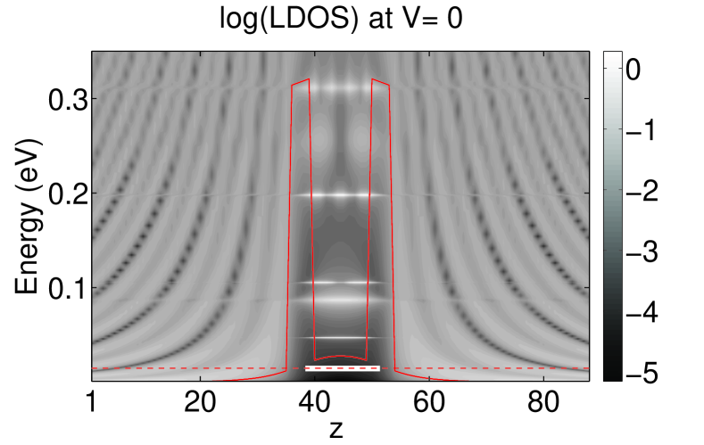
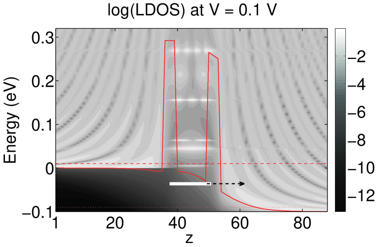

While (Ga,Mn)As inevitably is a disordered system, our starting point is an idealized system for which the valence band edge is identical to that of GaAs. Subsequently, valence band disorder is added in increasing steps allowing for a systematic qualitative account of its consequences on the IV-curve. For convenience we use an inverted hole energy scale but retain positively charged holes. In order to simulate the presence of MnGa impurity band levels, partially populated by holes, we use a positive (repulsive) charge background of cm-3 in the (Ga,Mn)As layer leading to an upward shift of the potential profile in the well region, as shown in Fig. 1. The local density of states of the ideal double-barrier structure (in absence of disorder) at zero bias and V, corresponding to the dominant current peak of the IV curve (see Fig. 5), is shown in Fig. 1 and Fig. 2, respectively. The resonant levels in the well are clearly visible and the solid line indicates the self-consistent potential profile of the structure. At zero bias the valence band edge of (Ga,Mn)As is lifted relative to that of the contact GaAs layers by about 30 meV thus partially aligning the MnGa levels (indicated schematically by the bold (white) solid line) with the chemical potential which, in turn, lies about 10 meV above the valence band edge of the GaAs leads. Therefore, when a bias greater than about 10 mV is applied the MnGa levels can no longer be filled resonantly from the emitter side and, beyond about 30 mV, no longer from either emitter or the collector. The latter situation is shown schematically in Fig. 2. This loss of holes from the MnGa levels in the well region and the insufficient resupply of holes from the GaAs emitter into the resonant valence band levels lead to a breakdown of ferromagnetic order in the (Ga,Mn)As well under small bias, i.e. a zero bias anomaly.
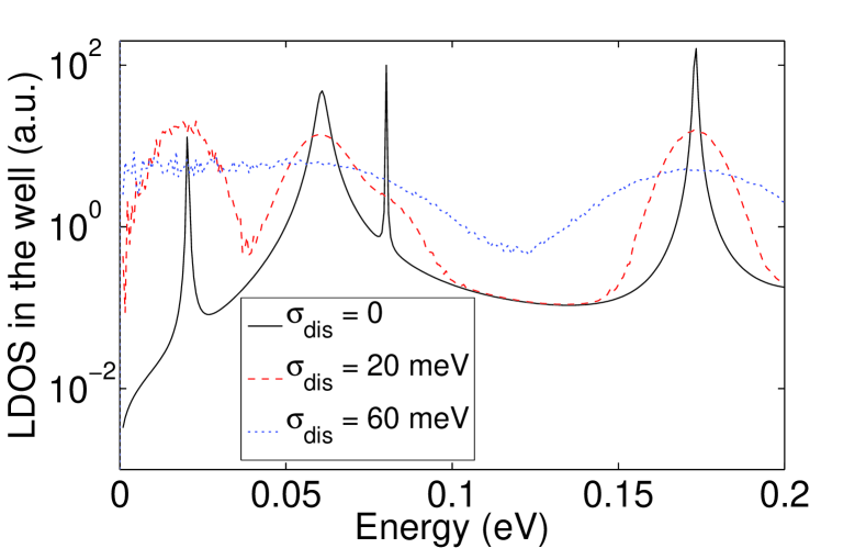
The transmission function and local density of states in the center of the Ga1-xMnxAs quantum well region is plotted for increasing degree of disorder in Fig. 3 and Fig. 4, respectively. Disorder leads to defect level in the band gap and a significant spectral broadening of the resonant levels associated with the lowest valence band resonances. Note also the strong increase of transmission probability in the low–bias regime from disorder, opened by resonances for tunneling.
As a key difference compared to the bulk (Ga,Mn)As situation, the hole density inside a (Ga,Mn)As quantum well is established by forming a steady state situation with the external leads. Since the Be doping level in the GaAs contacts is significantly lower than the Mn concentration this leads to a strongly reduced hole concentration (over bulk) in the (Ga,Mn)As wells under bias. Even under favorable bias conditions, in which resonant levels in the quantum well can be populated from the external leads, the quantum well hole density remains on the order of the hole density in the GaAs leads (in our case cm-3), which is at least two orders of magnitude smaller than in bulk (Ga,Mn)As. Therefore, in our simulations we find practically vanishing ferromagnetism (exchange splitting) for all bias values. In previous studies we have shown that for higher hole doping of the leads a bias-dependent ferromagnetic state with a maximum exchange splitting of the order of tens of meV can be expected, being detectable by a significant spin polarization of the collector current.Ertler and Pötz (2011, 2012) In this earlier study we focused on the transport through the first HH-subband using a simpler effective mass band model. The picture that the quantum well hole density is determined by the coupling to the leads surely applies to the case when the impurity band merges with the valence band, leading at most, to a broadening and shift of the valence band edge. In the presence of an isolated impurity band loosely bound holes may exist (at least at low voltages) in the confined impurity bands lying energetically below the first valence 2D-subband (on the inverted energy scale).
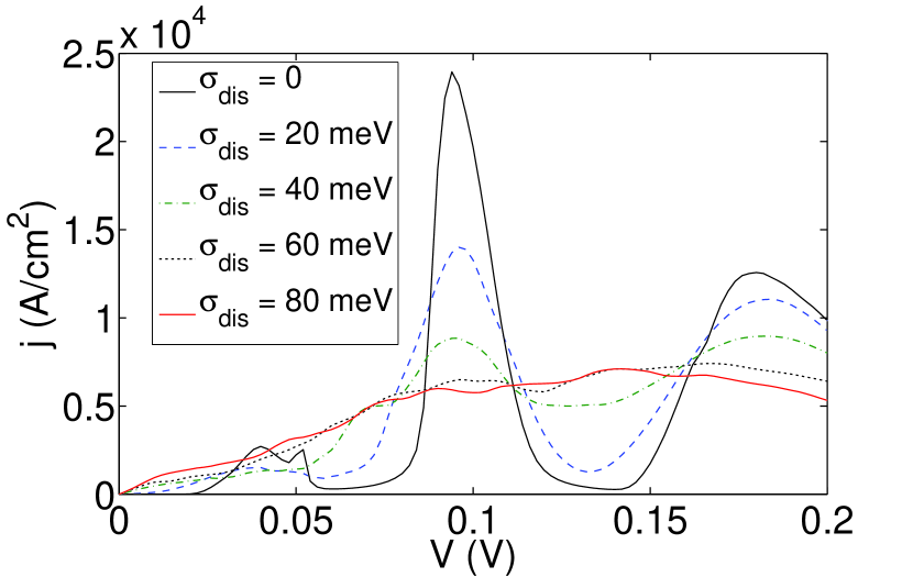
The main result of the paper is given in Fig. 5, which shows the IV-characteristics for increasing degree of disorder. Using a parallelized code typically 240 configurations are used for each characteristic, which needs about 4 days of computation on a 12-node Opteron server for a single IV-curve. For increasing disorder the resonances in the IV-curve become more and more broadened and start to overlap until they are almost washed out. Here a model which takes into account the HH-LH band mixing in the well is essential in order to see this effect. If ignored, the LH resonances would dominate the current magnitude compared to the HH peaks and regions of pronounced negative differential resistance would persist even for unphysically high degrees of disorder. For the low doping regime of the leads (relative to the Mn concentration in the quantum well), as considered here, we find an almost vanishing ferromagnetism ( meV) in the well leading to a vanishing current spin polarization. This results also suggest that, for a given (small) degree of disorder, enhancing the confinement, e.g. by using a thinner quantum well and/or higher barriers, should lead to smaller overlap between the subbands, thus enhancing resonant–tunneling features the IV-curve. Alternative external pressure may be used to enhance the splitting between the lowest HH and LH subbands.
IV Conclusions
In summary, we have shown that two factors can be relevant to understand the experimental findings of weak resonant–tunneling features and an absence of ferromagnetic order arising from thin (Ga,Mn)As quantum–well layers:
(i) The presence of considerable disorder in thin layers of (Ga,Mn)As which conspires with HH-LH band mixing in the quantum well to efficiently weaken any signatures of resonant tunneling in the IV characteristics.
(ii) The observed (almost) vanishing of ferromagnetic order in the (Ga,Mn)As quantum well can be understood by finding orders of magnitude lower hole densities in the well as compared to the bulk (Ga,Mn)As case of equal Mn concentration.
V Acknowledgment
We acknowledge helpful discussions with Prof. Masaaki Tanaka. This work has been supported by the Austrian Science Foundation under FWF project P21289-N16.
References
- Jungwirth et al. (2006) T. Jungwirth, J. Sinova, J. Mašek, J. Kučera, and A. H. MacDonald, Rev. Mod. Phys. 78, 809 (2006).
- Burch et al. (2008) K. S. Burch, D. D. Awschalom, and D. N. Basov, J. Magn. Magn. Mat. 320, 3207 (2008).
- Schneider et al. (1987) J. Schneider, U. Kaufmann, W. Wilkening, M. Baeumler, and F. Köhl, Phys. Rev. Lett. 59, 240 (1987).
- Jungwirth et al. (2007) T. Jungwirth, J. Sinova, A. H. MacDonald, B. L. Gallagher, V. Novák, K. W. Edmonds, A. W. Rushforth, R. P. Campion, C. T. Foxon, L. Eaves, et al., Phys. Rev. B 76, 125206 (2007).
- Richardella et al. (2010) A. Richardella, P. Roushan, S. Mack, B. Zhou, D. A. Huse, D. D. Awschalom, and A. Yazdani, Science 327, 665 (2010).
- Burch et al. (2006) K. S. Burch, D. B. Shrekenhamer, E. J. Singley, J. Stephens, B. L. Sheu, R. K. Kawakami, P. Schiffer, N. Samarth, D. D. Awschalom, and D. N. Basov, Phys. Rev. Lett. 97, 87208 (2006).
- Ohya et al. (2011) S. Ohya, K. Takata, and M. Tanaka, Nature Physics 7, 342 (2011).
- Ohya et al. (2007) S. Ohya, P. N. Hai, Y. Mizuno, and M. Tanaka, Phys. Rev. B 75, 155328 (2007).
- Ohya et al. (2010) S. Ohya, I. Muneta, P. N. Hai, and M. Tanaka, Phys. Rev. Lett. 104, 167204 (2010).
- Dietl and Sztenkiel (2011) T. Dietl and D. Sztenkiel, ArXiv e-prints (2011), eprint 1102.3267.
- Ohya et al. (2011) S. Ohya, K. Takata, I. Muneta, P. N. Hai, and M. Tanaka, ArXiv e-prints (2011), eprint 1102.4459.
- Madelung (1978) O. Madelung, Introduction to Solid-State Theory (Springer, Berlin, 1978).
- Likovich et al. (2009) E. Likovich, K. Russell, W. Yi, V. Narayanamurti, K.-C. Ku, M. Zhu, and N. Samarth, Phys. Rev. B 80, 201307(R) (2009).
- Miyazaki et al. (1987) S. Miyazaki, Y. Ihara, and M. Hirose, Phys. Rev. Lett. 59, 125 (1987).
- Li and Pötz (1993) Z. Q. Li and W. Pötz, Phys. Rev. B 47, 6509 (1993).
- Van Esch et al. (1997) A. Van Esch, L. Van Bockstal, J. De Boeck, G. Verbanck, A. S. van Steenbergen, P. J. Wellmann, B. Grietens, R. Bogaerts, F. Herlach, and G. Borghs, Phys. Rev. B 56, 13103 (1997).
- Das Sarma et al. (2003) S. Das Sarma, E. H. Hwang, and A. Kaminski, Phys. Rev. B 67, 155201 (2003).
- Ertler and Pötz (2011) C. Ertler and W. Pötz, Phys. Rev. B 84, 165309 (2011).
- Ertler and Pötz (2012) C. Ertler and W. Pötz, Journal of Computational Electronics pp. 1–7 (2012), ISSN 1569-8025.
- Luttinger and Kohn (1955) J. M. Luttinger and W. Kohn, Phys. Rev. 97, 869 (1955).
- Chao and Chuang (1991) C. Y.-P. Chao and S. L. Chuang, Phys. Rev. B 43, 7027 (1991).
- Dietl et al. (1997) T. Dietl, A. Haury, and Y. M. d’Aubigné, Phys. Rev. B 55, R3347 (1997).
- Jungwirth et al. (1999) T. Jungwirth, W. A. Atkinson, B. H. Lee, and A. H. MacDonald, Phys. Rev. B 59, 9818 (1999).
- Fabian et al. (2007) J. Fabian, A. Matos-Abiague, C. Ertler, P. Stano, and I. Žutić, Acta Physica Slovaca 57, 565 (2007).
- Datta (1995) S. Datta, Electronic Transport in Mesoscopic Systems (Cambridge University Press, Cambridge, England, 1995).
- López-Sancho et al. (1985) M. P. López-Sancho, J. M. López-Sancho, and J. Rubio, J. Phys. F: Met. Phys. 15, 851 (1985).
- Kaxiras (2003) E. Kaxiras, Atomic and Electronic Structure of Solids (Cambridge University Press, Cambridge, 2003).
- Ashcroft and Mermin (1976) N. W. Ashcroft and N. D. Mermin, Solid State Physics (Saunders, Philadelphia, 1976).