Force and conductance during contact formation to a molecule
Abstract
Force and conductance were simultaneously measured during the formation of Cu– and – contacts using a combined cryogenic scanning tunneling and atomic force microscope. The contact geometry was controlled with submolecular resolution. The maximal attractive forces measured for the two types of junctions were found to differ significantly. We show that the previously reported values of the contact conductance correspond to the junction being under maximal tensile stress.
pacs:
61.48.-c, 68.37.Ef, 68.37.Ps, 73.63.-b1 Introduction
When a molecule is contacted by electrodes to measure the conductance of the molecular junction, new bonds are formed and significant forces may arise. These forces affect the atomic-scale junction geometry, which is crucial for its transport properties [1, 2, 3, 4, 5]. Current and force can be measured simultaneously using a combination of scanning tunneling microscopy (STM) and atomic force microscopy (AFM). Such measurements were carried out for metallic contacts [2, 6, 7, 8, 9]. Related data was reported for contacts to single molecules in a liquid environment [10, 11] and for molecules on a metal surface [12]. However, the exact contact geometry was not accessible. 3,4,9,10-perylene-tetracarboxylicacid-dianhydride was probed in ultrahigh vacuum using AFM to controllably lift the molecule [13]. A bimodal distribution of conductances was observed and suggested to reflect two distinct bonding geometries. As to controlled molecule–molecule contacts, experimental results are few. The conductance of – contacts was measured by attaching a molecule to an STM tip and approaching a second molecule in a monolayer on Cu(111) [14]. The force between a metal tip and molecules in double layers on Cu(111) was addressed with AFM [16, 17]. While close distances well into the repulsive range were explored, the corresponding conductances [18] were significantly lower than in the STM work of Ref. [14]. A possible origin for this difference may be different geometries of the contact between the tip and the molecule in these experiments. Atomically sharp electrodes were shown to act as bottlenecks for charge injection into [15, 19]. While tips had been intentionally flattened to firmly attach a molecule in Ref. [14], the tip used in Ref. [16] presumably was atomically sharp. Another possible reason for reduced conductance is foreign material at the tip apex. Here, we present low-temperature force and conductance data for the controlled formation of Cu– and – contacts. The orientations of the molecules at the tip and the surface were determined from STM imaging. The elasticity of both contacts is analyzed and compared with density functional theory (DFT) calculations.
2 Experiment
Our experiments were performed with a homebuilt STM/AFM in ultrahigh vacuum at a temperature of . Clean Cu(111) surfaces were prepared by repeated sputtering and annealing cycles. Submonolayer amounts of were then deposited onto the sample by sublimation at room temperature. Subsequent annealing to led to a well-ordered structure of [20, 21, 22, 23]. After additional sublimation of small amounts of onto the cooled sample, isolated molecules were found on both the islands and the bare Cu substrate [24]. A PtIr tip was attached to the free prong of a quartz tuning fork oscillating with an amplitude of at its resonance frequency of . The tip was covered with Cu by repeated indenting into the substrate until submolecular resolution was achieved. The vertical force acting on the tip at the point of closest tip approach was calculated from the measured frequency shift (shown in S1) as a function of the vertical piezo displacement using the formalism of Sader and Jarvis [25]. Due to the limited bandwidth of the transimpedance amplifier, the current recorded with the oscillating tip is averaged over the entire range of oscillation. The non-averaged conductance was calculated using the method of Sader et al. [26], which recovers the instantaneous current at the point of closest tip approach. The bias voltage was applied to the sample. Further experimental details can be found in the supplementary data.
We note that the intrinsic energy dissipation of the tuning fork did not change significantly during the contact formation. In addition, STM images taken before and after the contact measurement showed no changes. These facts suggest that no inelastic deformations of tip or molecule occurred.
3 Cu– contacts
Figure 1(a) displays a typical constant-current STM image of a island used for contact measurements with Cu-covered tips. The island comprises two domains which differ by an azimuthal rotation of the - molecules by 60° (h0 and h60). molecules adsorbed on Cu(111) with either a hexagon (-) or a pentagon (-) facing up give rise to distinctly different patterns in the STM image [27]. Fig. 1(b) shows the different orientations of the molecules as viewed from the tip position. Double bonds separating two hexagons (6:6 bonds) are marked by red bars. Contact data recorded with a Cu tip above the center of a - molecule are shown in Fig. 1(c). Both the total interaction force (solid line) evaluated at the point of closest approach to the sample and the instantaneous conductance (dots) are displayed versus the piezo displacement . We first focus on the force, which is shown over a wider range of displacements in Fig. 1(d). To minimize the electrostatic force, which results from the contact potential difference, a bias voltage of was applied during the contact measurement [28, 29, 30]. At large tip–sample distances, reflects the long-range van-der-Waals force between the tip and the sample. It can be approximated by a power law [31] with typical fit parameters , , and (fit range: ). The fit is shown in Fig. 1(d) as a dashed line. The exponent close to 2 indicates an effective sphere–plane geometry of the junction.

The short-range force [dashed-dotted line in Fig. 1(d)], which only acts on the atoms in the immediate vicinity of the molecular junction, is estimated as . It is attractive for large tip heights, reaches a minimum at Å, and finally becomes repulsive for . The fitted van-der-Waals force at contact ( nN) is consistent with estimates for a sharp tip [32]. We note that the total force and the short-range force exhibit maximal attraction at nearly the same position In other words, long-range forces do not significantly affect the point of maximal attraction. However, they do affect the value of the maximal attraction. Using different tips we found it to scatter between and . We ascribe the origin of these significant short-range forces to the chemical bond formation between tip and molecule. Interestingly, calculated interaction forces for a Si tip and on Si(100) are in a very similar range () [32]. The data of - and - were very similar except for a shift of along the abscissa due to the different apparent heights of the molecules. This apparent insensitivity to the detailed bonding geometry may be attributed to the high reactivity of 6:6 bonds. It causes the Cu atom at the tip apex to laterally relax [19]. As a result, a 6:6 bond is most likely contacted independent of the orientation of the molecule. The conductance in Fig. 1(c) shows a typical transition from tunneling at small to electrical contact. To define the point of contact, the intersection of linear fits in the transition and contact regime is used [Fig. 1(c), dashed lines] [5]. The resulting contact conductance ( is the conductance quantum) is in agreement with previous experimental results [5, 14, 15]. Comparing the conductance data with the simultaneously measured force [Fig. 1(c), solid line] we find that the point of contact corresponds to maximal attractive force. The same observation is made for – contacts (see below). A similar result has been reported from metal–metal point contacts, where a maximal attractive force was measured at [9]. Modeling of metallic contacts also suggests that the deformation of the junction is maximal at the point of contact formation [33, 34]. Recently, two-level fluctuations of the conductance on a s time scale have been reported from on Cu(100) at the transition from tunneling to contact for a metal- contact [35]. In the present case of a structure of on Cu(111), and at the rather low bias voltages used (), such fluctuations were not observed [36].
4 - contacts
By approaching the tip sufficiently close, a single molecule was attached to the tip apex. The orientation of such tips was determined by ’reverse imaging’ on small Cu clusters which had been deposited before from the tip onto the bare Cu(111) surface [14, 15]. Constant-current images of such a Cu cluster recorded at reveal the second lowest unoccupied orbital (LUMO+1) of the molecule [14]. Compared to normal STM images of the LUMO+1 [Fig. 1(a)], they show a mirror image of the molecule [37].
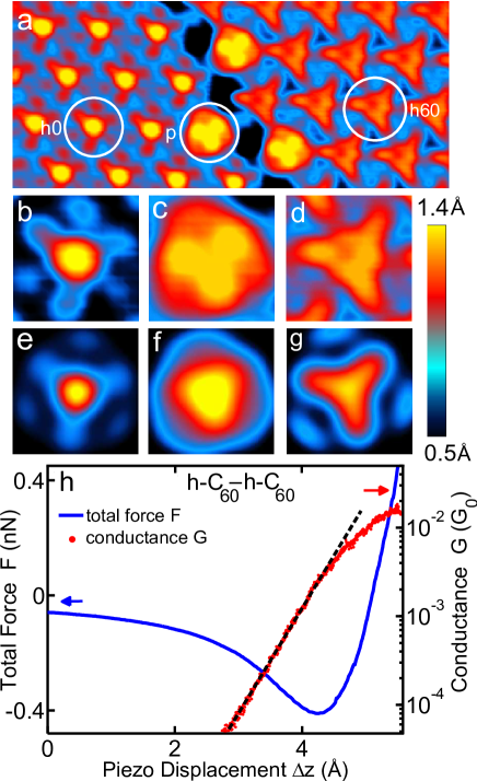
The relative orientations of the tip and sample molecules strongly affect the conductance of the junction in the tunneling range. Figure 2(a) shows a island imaged using a -functionalized tip with a hexagon facing towards the surface (- tip). Similar to Fig. 1(a), the island comprises two rotational domains of - (h0 and h60), as well as a few - molecules. Owing to the different orientations, distinctly different patterns are observed with the - tip for h0, p, and h60 molecules [Figs. 2(b–d)]. For example, the center of - appears either as a maximum (h0) or as a minimum (h60) in the STM image. On -a threefold symmetry of the - tip is clearly discernible, which reflects the 5:6 bonds of the molecule at the tip. The symmetries of these patterns can be understood from a convolution of the local densities of electronic states (LDOS) of the tip and the sample. At electrons essentially tunnel from the highest occupied molecular orbital (HOMO) of the - tip to the lowest unoccupied molecular orbital (LUMO) of the molecule at the surface. A two-dimensional convolution of these orbitals according to the orientations given in Fig. S2 is shown in Figs. 2(e–g) [37]. It reproduces the experimental data with the best agreement obtained for the h0 pattern.
Figure 2(h) displays the force (solid line) and the conductance (dots) measured on a - molecule with a - tip at an applied voltage of . Compared to the data from a Cu tip [Fig. 1(c)], the maximal attractive force is smaller by a factor of 4. In experiments with different tips, this maximal attractive force varied from to . In part, this scatter may be attributed to the uncertainty of the lateral tip position, which we estimate to be of a diameter. The conductance measured for a – contact [Fig. 2(h), dots] starts to deviate from a purely exponential behavior (dashed line) at a piezo displacement close to the position of the maximum of the attractive force. The conductance at this point () is approximately two orders of magnitude smaller than with a Cu tip [14]. When we approached the tip further towards the surface until the total force exceeded , a rotation of the molecule at the tip occurred.
5 Comparison of elasticities of Cu– and - contacts
The forces at the junction cause atomic relaxations which affect the conductance. Below, a simple model is used to estimate the deformation of the junction from the measured conductance and force data. First, the conductance of a rigid junction is calculated as a function of the piezo displacement, [14, 37], which is shown in Fig. 7.
The junction deformation is approximated by a linear relation , using the experimentally determined force . We then obtain the theoretical conductance of the deformed junction, , which depends on the stiffness of the junction :
| (1) |
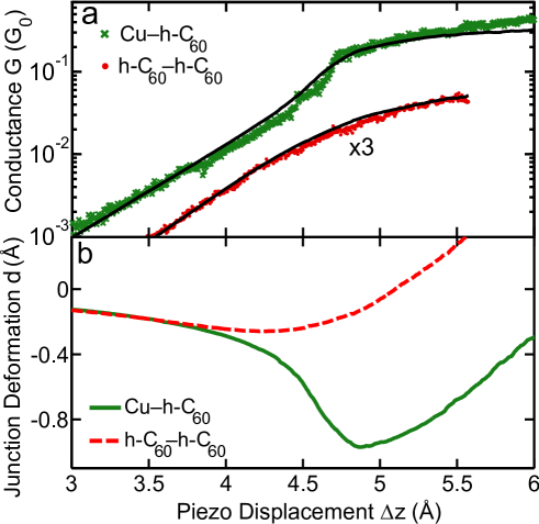
From a fit of to the measured data [Figs. 1(c) and 2(h)] the stiffness is obtained. Figure 3(a) shows fits (solid lines) for Cu–- (crosses) and -–- (dots) contacts. Cu–- data (not shown) yield similar results. From measurements with different tips we determined elasticities for Cu– and for –. The extracted deformation shown in Fig. 3(b) corresponds to a reduction of the tip–molecule distance of for the Cu– contact (solid line). For the – contact (dashed line), is smaller () and the transition from tensile to compressive deformation occurs within the range that was accessible in our experiment. While the deformations are smaller than the values reported for metal contacts [9, 33, 38], they still significantly affect the conductance.
The values for may be interpreted in terms of the elasticities of the components of the junctions. DFT calculations taking into consideration several atomic configurations were used to estimate elasticities of tip and sample (see appendix A). As summarized in Tab. 1, we find that a metallic Cu tip can be characterized by a stiffness in the range depending on its atomistic structure and on details of the calculational scheme. For the sample we find for - or - on reconstructed Cu(111) [23]. Combining tip and sample elasticities in series, we thus estimate for a Cu– contact. Similarly, for a --tip we find , which leads to for a -–- contact. For both contacts, the experimentally determined elasticity is softer than the calculated one by a factor of 2. We attribute this difference to two main factors: First, the elasticity calculations can be considered as upper bounds as only a finite number of degrees of freedom are taken into account (see appendix A). Second, the elasticity estimates above do not take into account the softening of the springs close to contact due to the formation of chemical bonds between tip and sample.
It is instructive to compare the obtained junction stiffness values with that of an isolated molecule. From our DFT calculations we find that squeezing a molecule between two opposite hexagons corresponds to a spring constant of 222 N/m (appendix A), i.e., the elasticity of a is significantly stiffer than the molecular junctions considered in this study. The junction deformation therefore mainly involves the metal-molecule bonds and the STM tip.
6 Conclusions
In summary, simultaneous force and conductance measurements for Cu– and – contacts have been performed. Angstrom-scale deformations of the contacts and effective stiffness extracted from the experimental data agree with elasticities determined with DFT calculations. We find that the maximal attractive force measured at a – contact is 4 times smaller than in a Cu– junction. Moreover, the force data reveal that previously reported contact conductances correspond to geometries in which the junctions are under maximal tensile stress.
Acknowledgments
We thank C. González and N. L. Schneider for discussions. Financial support by the Deutsche Forschungsgemeinschaft (SFB 677), the Innovationsfonds Schleswig-Holstein, and the EU projects HERODOT and ARTIST is acknowledged.
Appendix
Appendix A DFT calculations
In order to estimate the elasticities related to the experimental sample and tip sides we considered the generic structures shown in Fig. 4. Calculations were performed using the SIESTA [39] pseudopotential density functional theory method with the PBE-GGA exchange-correlation functional [40], a 400 Ry mesh cutoff, and a Monkhorst-Pack [41] -mesh. The Fermi surface was treated by a second-order Methfessel-Paxton [42] scheme with an electronic temperature of 300 K. The basis set consisted of default double-zeta plus polarization (DZP) orbitals for C and Cu atoms generated with an energy shift of 0.01 Ry. The force tolerance for the structural optimizations was 0.02 eV/Å. The total energies from SIESTA were not corrected for basis set superposition errors. Two different lattice constants for the Cu crystal ( Å and Å) were considered to confirm that the results do not depend sensitively on this parameter.
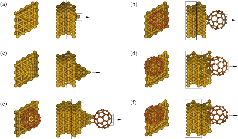


The computational procedure consisted of the following steps: (1) Relaxation of initial geometry with the boxed atoms in the Cu slab (Fig. 4) kept fixed at bulk coordinates while the other degrees of freedom fully relaxed. (2) Displacement of the topmost atoms (box with arrow in Fig. 4) perpendicular to the surface film while relaxing all remaining degrees of freedom.
| Figure | System | |||
|---|---|---|---|---|
| (Å) | (N/m) | (N/m) | ||
| 5(a) | Cu-adatom | 3.70 | 52 (55) | |
| 5(b) | --flat | 3.70 | 81 (78) | |
| 5(c) | Cu-pyramid | 3.62 | 50 (44) | 49 (51) |
| 3.70 | 47 (45) | 49 (47) | ||
| 5(d) | --reconst | 3.62 | 129 (129) | |
| 3.70 | 129 (112) | |||
| 5(e) | --tip | 3.70 | 57 (53) | 54 (43) |
| 5(f) | --reconst | 3.62 | 131 (118) | |
| 6 | Isolated | 222 (240) |
The energy costs associated with the deformations with respect to the displacement of the topmost atoms are shown in Fig. 5 with being the relaxed junction. For , tensile strain is exerted on the system. Quadratic (as well as fifth order) fits to these energy differences yield the effective spring constants in Tab. 1. It should be noted that the elasticities in Tab. 1 represent in fact upper bounds because of the limited size of the unit cell. In the real system more atoms respond to the pull on the topmost atoms, which leads to a smaller effective spring constant.
To test the accuracy of the SIESTA calculations, selected checks with the VASP code based on a plane-wave basis and the projector-augmented wave method (PAW) [43, 44, 45] were also performed. We used PBE-GGA [40], at least 400 eV energy cutoff, a (or ) Monkhorst-Pack [41] -mesh, first-order Methfessel-Paxton [42] scheme with 0.05 eV smearing width, and 0.02 eV/Å force tolerance. As seen in Fig. 5 and Tab. 1, the two codes yield similar estimates of the elasticities.
To determine effective elasticities for the combined elasticity of tip and sample the springs from Tab. 1 are added in series. In this way, for a Cu-adatom [Fig. 4(a)] or for a sharp pyramidal Cu-tip [Fig. 4(c)] in contact with a - on reconstructed Cu(111) [Fig. 4(d)], we obtain . In the case of the contact between a Cu tip [Fig. 4(a) or (c)] and a - on the flat Cu(111) [Fig. 4(b)], an effective elasticity of is obtained. Due to the reduced number of bonds of - on flat Cu(111) in comparison with - on reconstructed Cu(111), is smaller. Similarly, for the -tip [Fig. 4(b) or (e)] in contact with a - on reconstructed Cu(111), we estimate .
We also analyzed the stiffness of an isolated molecule with SIESTA, cf. Fig. 6. By controlling the distance between two opposing hexagons while relaxing all other degrees of freedom we obtain an effective stiffness of the molecule of N/m. A comparable (but slightly larger) stiffness of N/m is obtained when considering only a deformation along the characteristic elongation/compression H vibrational mode [Fig. 6(c)]. Deforming along the isotropic A vibrational mode [Fig. 6(d)] yields a much larger stiffness ( N/m).
Appendix B Elasticity model
The influence of the junction deformation on the conductance is described as follows. First, the conductance of a rigid system as a function of the piezo displacement, , is calculated for Cu–- and – contacts (Figs. 7(a) and (b)). corresponds to a distance between the topmost tip atom and the topmost -hexagon of in the Cu–- contact and to a – center distance of in the – contact. Further calculational details can be found in Ref. [14].
Next, we assume that the deformation depends linearly on the experimentally determined force, i. e. with describing the effective stiffness of the junction. The theoretical conductance of the deformed junction, , depending on is given by:
| (2) |
The interpolated calculated conductance is then fitted to the experimental conductances . As the absolute tip–sample distance was unknown in the experiments, an arbitrary shift on the abscissa for is allowed. This shift is already comprised in Fig. 7, so that the axes in Fig. 7(a) and (b) correspond to the axis in Fig. 3.

Fits for the Cu–- and – contacts shown in Fig. 3(a) and to similar data calculated for other microscopic tips yield and , respectively. Compared to the values from the DFT calculations in appendix A, the effective spring constants qualitatively agree, but are smaller by a factor of 2. This deviation is not unexpected since the calculated elasticities are upper bounds. Furthermore, the model neglects the formation of chemical bonds between tip and sample, which are expected to weaken the effective spring constant.
References
References
- [1] Cross G, Schirmeisen A, Stalder A, Grütter P, Tschudy M and Dürig U 1998 Phys. Rev. Lett. 80 4685
- [2] Rubio-Bollinger G, Joyez P and Agraït N 2004 Phys. Rev. Lett. 93 116803
- [3] Limot L, Kröger J, Berndt R, Garcia-Lekue A and Hofer W A 2005 Phys. Rev. Lett. 94 126102
- [4] Chen F, Hihath J, Huang Z, Li X and Tao N 2007 Annu. Rev. Phys. Chem. 58 535–564
- [5] Nel N, Kröger J, Limot L, Frederiksen T, Brandbyge M and Berndt R 2007 Phys. Rev. Lett. 98 065502
- [6] Schirmeisen A, Cross G, Stalder A, Grütter P and Dürig U 2000 New J. Phys. 2 29
- [7] Sun Y, Mortensen H, Schär S, Lucier A S, Miyahara Y and Grütter P 2005 Phys. Rev. B 71 193407
- [8] Sawada D, Sugimoto Y, Morita K, Abe M and Morita S 2009 Appl. Phys. Lett. 94 173117–173117–3
- [9] Ternes M, González C, Lutz C P, Hapala P, Giessibl F J, Jelínek P and Heinrich A J 2011 Phys. Rev. Lett. 106 016802
- [10] Xu B, Xiao X and Tao N J 2003 J. Am. Chem. Soc. 125 16164–16165
- [11] Ebeling D, Oesterhelt F and Hölscher H 2009 Appl. Phys. Lett. 95 013701
- [12] Lantz M A, O’Shea S J and Welland M E 1999 Surf. Sci. 437 99–106
- [13] Fournier N, Wagner C, Weiss C, Temirov R and Tautz F S 2011 Phys. Rev. B 84 035435
- [14] Schull G, Frederiksen T, Brandbyge M and Berndt R 2009 Phys. Rev. Lett. 103 206803
- [15] Schull G, Frederiksen T, Arnau A, Sáchez-Portal D and Berndt R 2011 Nature Nano. 7, 23–27
- [16] Pawlak R, Kawai S, Fremy S, Glatzel T and Meyer E 2011 ACS Nano 5 6349–6354
- [17] Pawlak R, Kawai S, Fremy S, Glatzel T and Meyer E 2012 J. Phys.: Condens. Matter 24 084005
- [18] The current shown in Ref. [16] appears to represent the average over an oscillation cycle of the vibrating AFM tip. From this data the instantaneous current at the point of closest approach of the tip to the sample, which may be compared to the current in an STM, can be estimated using the method by Sader and Sugimoto [26].
- [19] Schull G, Dappe Y J, González C, Bulou H and Berndt R 2011 Nano Letters 11 3142–3146
- [20] Hashizume T, Motai K, Wang X D, Shinohara H, Saito Y, Maruyama Y, Ohno K, Kawazoe Y, Nishina Y, Pickering H W, Kuk Y and Sakurai T 1993 Phys. Rev. Lett. 71 2959
- [21] Pai W W, Hsu C, Lin M C, Lin K C and Tang T B 2004 Phys. Rev. B 69 125405
- [22] Wang L and Cheng H 2004 Phys. Rev. B 69 045404
- [23] Pai W W, Jeng H T, Cheng C, Lin C, Xiao X, Zhao A, Zhang X, Xu G, Shi X Q, Hove M A V, Hsue C and Tsuei K 2010 Phys. Rev. Lett. 104 036103
- [24] Larsson J A, Elliott S D, Greer J C, Repp J, Meyer G and Allenspach R 2008 Phys. Rev. B 77 115434
- [25] Sader J E and Jarvis S P 2004 Appl. Phys. Lett. 84 1801–1803
- [26] Sader J E and Sugimoto Y 2010 Appl. Phys. Lett. 97 043502
- [27] Silien C, Pradhan N A, Ho W and Thiry P A 2004 Phys. Rev. B 69 115434
- [28] Nonnenmacher M, O’Boyle M P and Wickramasinghe H K 1991 Appl. Phys. Lett. 58 2921
- [29] Kitamura S, Suzuki K and Iwatsuki M 1999 Appl. Surf. Sci. 140 265–270
- [30] Okamoto K, Sugawara Y and Morita S 2002 Appl. Surf. Sci. 188 381–385
- [31] Israelachvili J N 1992 Intermolecular & Surface Forces 2nd ed (San Diego: Academic Press)
- [32] Hobbs C and Kantorovich L 2006 Surf. Sci. 600 551–558
- [33] Olesen L, Brandbyge M, Sørensen M R, Jacobsen K W, Lægsgaard E, Stensgaard I and Besenbacher F 1996 Phys. Rev. Lett. 76 1485–1488
- [34] Trouwborst M L, Huisman E H, Bakker F L, van der Molen S J and van Wees B J 2008 Phys. Rev. Lett. 100 175502
- [35] Nel N, Kröger J and Berndt R 2011 Nano Lett. 11 3593–3596
- [36] Schneider N L: A private communication
- [37] See supplementary data for details.
- [38] Hofer W A, Fisher A J, Wolkow R A and Grütter P 2001 Phys. Rev. Lett. 87 236104
- [39] Soler J, Artacho E, Gale J D, Garcia A, Junquera J, Ordejon P and Sanchez-Portal D 2002 J. Phys.: Condens. Matter 14 2745–2779
- [40] Perdew J P, Burke K and Ernzerhof M 1996 Phys. Rev. Lett. 77 3865
- [41] Monkhorst H J and Pack J D 1976 Phys. Rev. B 13 5188
- [42] Methfessel A and Paxton A T 1989 Phys. Rev. B 40 3616
- [43] Kresse G and Hafner J 1993 Phys. Rev. B 47 558
- [44] Kresse G and Furthmüller J 1996 Phys. Rev. B 54 11169
- [45] Kresse G and Joubert D 1999 Phys. Rev. B 59 1758