Two opposite hysteresis curves in semiconductors with mobile dopants
Abstract
Recent experimental researches on semiconductors with mobile dopants (SMD) have reported unconventional hysteretic current-voltage (-) curves, which form dynamically in either one of the two opposite directions, the counter-figure-eight and figure-eight ways. However the fundamental theory for the formation of the two directions is still absent, and this poses a major barrier for researches oriented to applications. Here, we introduce a theoretical model to explain the origin of the two directions, and find that the two ways originate from the spatial inhomogeneity of the dopant distribution in SMD. The counter-figure-eight (figure-eight) way of the hysteretic curve is obtained when dopants are driven from far from (near) the Schottky interface to the opposite side in the SMD. This finding indicates that the directions of hysteretic curve in SMD can be controlled.
pacs:
73.40.Sx,68.47.Fg,73.30.+yThe successful application of semiconductor devices over a wide range of electronic devices is attributable to their unique electrical properties, which are sensitive to the configuration of their dopants. Generally, dopants are assumed to be immobile. What happens if the dopants are mobile? Recent research on semiconductors with mobile dopants (SMD) such as oxygen vacancies () Waser2007 ; Yang2009 indicates that SMD demonstrates its conductance change due to the alteration of the dopant distribution in SMD HPnature2008 . As an example, consider a metal(M)-semiconductor(S) Schottky contact (n-type) as shown in Fig. 1(a). When a positive (negative) external bias is applied to the metal, the dopants are pushed away from (attracted toward) the metal, as a result, the dopant distribution is non-uniformly altered. Because the interfacial band structure of a semiconductor is sensitive to the concentration of the dopants, different dopant distribution causes different conductance state of the semiconductor. This conductance change is applicable to various fields of science and engineering such as resistive switching phenoemena Waser2009R , memristive system HPnature2008 , neuroscience neuro1 , and non-volatile memory devices Yang2008 ; Janousch ; Nian ; MJLee2011 , and thus it has received great interests.
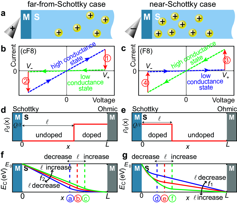
Such conductance change results in a hysteretic current-voltage (-) curve. One conventional explanation for the hysteretic curve is as follows Yang2009 . When a positive (negative) bias () is applied, the donor concentration becomes low (high) near the Schottky interface. Then the Schottky barrier width increases (descreases) because Sze , thus, the conductance decreases (increases) as denoted by \footnotesize1⃝ (\footnotesize2⃝) in Fig. 1(b). This directional hysteretic curve is called the counter-figure-eight (cF8) curve Shibuya and has been found in many materials Janousch ; MJLee2011 ; Szot .
However, the opposite way of curve (Fig. 1(c)), called the figure-eight (F8) curve, has also been reported in many literatures Yang2008 ; Sawa ; Sawa2 . Moreover, the coexistence of both directions in a single sample has been reported Yang2009 ; Muen ; Shibuya . To understand the origin of the two directions, several experiments and heuristic arguments have been presented. For example, Yang et al. Yang2009 suggested that the cF8 and F8 curves are derived from the top and bottom Schottky interfaces, respectively. However, Shibuya et al. Shibuya hypothesized that the cF8 curve arises from movement through conducting filaments inside the sample, whereas the F8 curve has a purely electronic origin. Subsequently, the same authors suggested that the cF8 and F8 curves originate from the respective inhomogeneous (or filamentary) and homogeneous distributions of parallel to the interface Muen .
Despite these experimental results and heuristic arguments, the origin of the two ways of hysteretic - curves has not been elucidated theoretically yet. In this Letter, we theoretically demonstrate that the two ways of - hysteretic curves intrinsically appear in the SMD, resulting from the spatial inhomogeneous distribution of dopants. When most dopants are located far from (near) the Schottky interface, the cF8 (F8) curve appears.
We first introduce a simple theoretical model in one dimension to illustrate the mechanism of the two ways in SMD depending on the initial dopant distribution. In this model, the semiconductor is in contact with the metals located at and to form the Schottky and Ohmic interfaces (Fig. 1(d)) with the boundary conditions and , respectively. We consider two different cases of initial dopant density distributions: dopants are located 1) far from (Fig. 1 (d)) and 2) near (Fig. 1 (e)) the Schottky interface. For simplicity, we assume that the dopant density distribution is constant in space. Then, for doped region, in the region [, ] for the far-from-Schottky case and in [, ] for the near-Schottky case, where is the total amount of dopants in a semiconductor and assumed to be a conserved quantity. For undoped region, . This simplification is very useful to capture the essential mechanism of the two ways of the hyteresis curves. We assume that the electrons are fully depleted in the doped region for analytic calculation. Non-constant case and not-fully depleted cases will be treated numerically later. Under this simplified circumstance, the position-dependent conduction band can then be calculated by solving the Poisson’s equation Neamen , , where is the electronic charge, is the space charge density, and is the permittivity of the semiconductor. Note that , where is the dopant charge. Here, we deal with the case (n-type semiconductor).

We first consider the far-from-Schottky case. The Poisson’s equations for in the regions and become and , respectively. Using the boundary conditions, and , and continuity at , we can easily obtain in the whole range. Particularly for , we obtain that
| (1) |
Here, is the slope of in the undopped region. If is initially located at \footnotesizea⃝ in Fig. 1(f) and a positive bias is applied, increases as the direction \footnotesizea⃝\footnotesizeb⃝\footnotesizec⃝. Then increases or the slope in the undopped region becomes less steeper (Eq. (1)) as shown in Fig. 1(f), which makes the Schottky barrier width thicker. Therefore, the conductance decreases, which corresponds to the conductance change denoted by \footnotesize1⃝ in Fig. 1(b). If a negative bias is applied to this low conductance state, will change reversely as \footnotesizec⃝\footnotesizeb⃝\footnotesizea⃝. Then the conductance increases as denoted by \footnotesize2⃝ in Fig. 1(b). This result agrees with the conventional explanation for cF8 curve.
For the near-Schottky case, the calculation for can be performed similarly. The Poisson’s equations for and become and , respectively. For , we obtain that
| (2) |
If initial is located at \footnotesized⃝ in Fig. 1(g), makes increase as the direction \footnotesized⃝\footnotesizee⃝\footnotesizef⃝. Then, by the similar explanation as the far-from-Schottky case, becomes thinner as shown in Fig. 1(g) and the conductance increases, which corresponds to the conductance change denoted by \footnotesize3⃝ in Fig. 1(c). If is applied to this high conductance state, reverse process occurs, which causes the conductance decreases as denoted by \footnotesize4⃝ in Fig. 1(c). Therefore, this result verifies that F8 curve intrinsically appears in SMD without the assumption of the electronic function or the two Schottky interfaces.

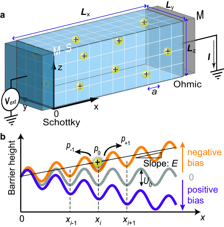
Using numerical simulation, now, we will show that the above analysis is still valid without the assumptions of non-uniform and not-fully depleted doped region. For quantitative calculation, we use the parameters for Pt-SrTiO3 contact. Let us consider a three-dimensional lattice (lattice constant nm) whose lengths in -, -, and -directions are , , and , respectively, as shown in Fig. 2(a). Here, nm for manageable calculation. Two different metals are in contact with the lattice at and forming Schottky and Ohmic contacts, respectively. Donors () were distributed on the lattice depending on . Then the position-dependent conduction band can be calculated numerically by solving the Poisson’s equation, . However, the calculation of is not straightforward because . Therefore, we use the self-consistent relaxation method to obtain and simultaneously; we divide into two parts: , where and are the densities of positive and negative charges, respectively. When the density of donors is sufficiently high compared with the hole density, . corresponds to the density of electrons and is determined by the following equation Sze : where is the inverse temperature and is the effective density of the states in the conduction band. We used because for many semiconductors Neamen . We also confirmed that the essential feature of the simulation is not changed by variation of . Note that we set in the semiconductor and assume that the barrier height at the M-S interface is independent of the dopant density Shang . Thus, we can set up the boundary conditions at (ideal Schottky) and (ideal Ohmic) interfaces as eV Robertson and , respectively. Here, we neglect the image-charge effect for the sake of simplicity. Inserting and into the Poisson’s equation, we obtain and simultaneously. To confirm the validity of this technique, we calculate for a silicon semiconductor with various doping concentrations. The results are presented in Supplemental Material (SM) 1. The resulting describes the conduction band which is distorted in the insulating region of the Schottky barrier.
Next, using the obtained , the electric current of the major carriers (i.e., electrons) can be estimated with the following formula Straton :
| (3) | |||||
where is the free electron mass, is Planck’s constant, and . is the transition probability that an electron with -directional energy will tunnel through the Schottky barrier at and . In the discrete lattice, can be written as where the summation index extends over all cases satisfying and .
We assume a simple hopping motion along the -direction for the donors under a periodic potential with a barrier height , as shown in Fig. 2(b), because it is widely accepted that must overcome an energy barrier to move to the next lattice site Zhang . We also assume that a constant electric field is formed throughout the semiconductor when is applied between two electrodes. The validity of the constant -field approximation is discussed in SM2. Thus, when a negative (positive) is applied, the periodic potential energy for the donors increases (decreases) with a slope of , as shown in Fig. 2(b). Then, the heights of the left and right energy barriers, compared to the local minimum, become approximately and , respectively. The probability of remaining at the original site () is given by the probability that the donor cannot overcome a lower barrier among the two. So, . When , the probability of moving to site () is the half of the probability that the donor overcomes the left or higher barrier (another half of the probability should be counted for moving to the opposite direction). So, . Then . Similarly, when , and . By combining these two cases, we obtain
| (4) |
where , , and when , , and , respectively. For simplicity, we consider only a hardcore repulsion interaction between the two donors. Here, we adopt the thermal acceleration mechanism applied for SrTiO3 Menzel . So, high temperature eV-1 ( K) can be used for our simulation with eV Menzel . From Eq. (4) it is obvious that transformations as , , and do not change the hopping probabilities. Thus, we use eV-1 ( K) and eV instead of eV-1 and eV. Here, the attempt frequency for the hopping is Hz Jeon .
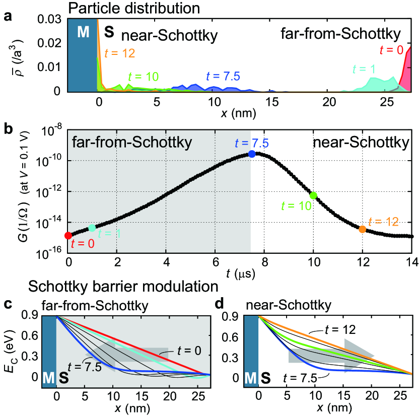
Using the above equations, the case in which the donors move from the Ohmic to the Schottky interface can be simulated. Initially, the donors were uniformly distributed with a density of Menzel . Using Eq. (4), we pushed the donors toward the Ohmic interface by applying a positive bias, the red curve in Fig. 3(a). Then, we applied a negative voltage V to attract donors towards the Schottky interface. Here, the donor density at is defined as , where is the number of donors at the plane. Here, Berg in high electric field ( the permittivity in free space), with periodic boundary conditions in the - and -directions. Fig. 3(a) shows the time-dependent distribution of the donors. The distribution moved toward the Schottky interface over time.

The conductance during the attraction process is calculated at V as a function of time . As indicated in Fig. 3(b), the - plot can be divided into two regions: for , increases as a function of , and for , decreases. When comparing the distributions shown in Fig. 3(a), increased (decreased) when most dopants were distributed in the far-from-Schottky (near-Schottky) region.
The two different -dependences of come from the different modulation behaviors of the Schottky barrier during the attranction process. For each , we obtained by calculating at and averaging over and . Fig. 3(c) shows when most dopants were distributed in the far-from-Schottky region (i.e., ). In this case, the pulling of the donors toward the Schottky interface resulted in a decrease in the Schottky barrier width, and increased. Fig. 3(d) presents the case where most dopants were distributed in the near-Schottky region (i.e., ). In this case, the attraction of the donor increased the Schottky barrier width rather than decreasing it. These results agree with those of the one-dimensional SMD model.
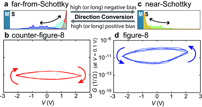
We also simulated - curves under a repetitive voltage sweep, with different initial donor distributions. Here, it took s for each voltage point and voltage gap is V. During the voltage sweep, is calculated at V. When most donors were initially distributed in the far-from-Schottky (near-Schottky) region as shown in Fig. 4(a) (Fig. 4(c)), decreases (increases) at positive bias and increases (decreases) at negative bias as shown in Fig. 4(b) (Fig. 4(d)), which corresponds to the direction of Fig. 1(b) (Fig. 1(c)) (see also movie clips). Furthermore, the direction of the - curve can be changed by applying a large bias, as indicated in Fig. 4.

In conclusion, we introduced the SMD model which demonstrates that two opposite hysteresis curves intrinsically appear in the SMD due to the inhomogeneous dopant density distriubtion. From this theoretical analysis, we can control the type of the - curve by modulating the mobile dopant distribution. The theoretical result we obtained in the Letter may become a fundamental basis for further development of SMD.
This research was supported by the National Research Foundation of Korea, Grants No. 2010-0015066 (B.K.), No. 2010-0020416 (T.W.N.), and No. NRF-2011-35B-C00014 (J.S.L.) and by the NAP of the Korean Research Council of Fundamental Science and Technology (B.K.).
References
- (1) R. Waser and M. Aono, Nature Mater. 6, 833-840 (2007).
- (2) J. J. Yang, J. Borghetti, D. Murphy, D. R. Stewart, and R. S. Williams, Adv. Mater. 21, 3754-3758 (2009).
- (3) D. B. Strukov, G. S. Snider, D. R. Stewart, and R. S. Williams, Nature 453, 80-83 (2008).
- (4) R. Waser, R. Dittmann, G. Staikov, and K. Szot, Adv. Mater. 21, 2632 R (2009).
- (5) D. B. Strukov, Nature 476, 403 (2011).
- (6) J. J. Yang, M. D. Pickett, X. Li, D. A. A. Ohlberg, D. R. Stewart, R. S. Willams, Nature Nanotech. 3, 429-433 (2008).
- (7) M. Janousch, G. I. Meijer, B. Delley, S. F. Karg, and B. P. Andreasson, Adv. Mater. 19, 2232-2235 (2007).
- (8) Y. B. Nian, J. Strozier, N. J. Wu, X. Chen, and A. Ignatiev, Phys. Rev. Lett. 98, 146403 (2007).
- (9) M.-J. Lee et al., Nature Mater. 10, 625-630 (2011).
- (10) S. M. Sze and K. K. Ng, Physics of Semiconductor Devices 3rd ed. Ch. 1 (Willey, New Jersey, 2007).
- (11) K. Shibuya, R. Dittmann, S. Mi, and R. Waser, Adv. Mater. 22, 411-414 (2010).
- (12) K. Szot, W. Speier, G. Bihlmayer, and R. Waser, Nature Mater. 5, 312-320 (2006).
- (13) A. Sawa, T. Fujii, M. Kawasaki, and Y. Tokura, Appl. Phys. Lett. 85, 4073-4075 (2004).
- (14) A. Sawa, T. Fujii, M. Kawasaki, and Y. Tokura, Appl. Phys. Lett. 88, 232112 (2006).
- (15) R. Muenstermann, T. Menke, R. Dittmann, and R. Waser, Adv. Mater. 22, 4819-4822 (2010).
- (16) D. A. Neamen, Semiconductor Physics and Devices Basic Principles, 3rd ed. Ch.9 (McGraw–Hill, New York, 2003).
- (17) D. S. Shang, J. R. Sun, L. Shi, and B. G. Shen, Appl. Phys. Lett. 93, 102106 (2008).
- (18) J. Robertson and C. W. Chen, Appl. Phys. Lett. 74, 1168 (1999).
- (19) R. Straton, J. Phys. Chem. Solids 23, 1177-1190 (1962).
- (20) Z. Zhang, Q. Ge, S.-C. Li, B. D. Kay, J. M. White, and Z. Dohnalek, Phys. Rev. Lett. 99, 126105 (2007).
- (21) S. Menzel, M. Waters, A. Marchewka, U. Böttger, R. Dittmann, and R. Waser, Adv. Funct. Mater. 21, 4487-4492 (2011).
- (22) S. H. Jeon, W. –J. Son, B. H. Park, and S. Han, Appl. Phys. A 102, 909–914 (2011).
- (23) R. A. van der Berg, P. W. M. Blom, J. F. M. Cillessen, and R. M. Wolf, Appl. Phys. Lett. 66, 697 (1995).