Tunable nano Peltier cooling device from geometric effects using a single graphene nanoribbon
Abstract
Based on the phenomenon of curvature-induced doping in graphene we propose a class of Peltier cooling devices, produced by geometrical effects, without gating. We show how a graphene nanoribbon laid on an array of curved nano cylinders can be used to create a targeted and tunable cooling device. Using two different approaches, the Nonequlibrium Green’s Function (NEGF) method and experimental inputs, we predict that the cooling power of such a device can approach the order of , on par with the best known techniques using standard superlattice structures. The structure proposed here helps pave the way toward designing graphene electronics which use geometry rather than gating to control devices.
As electronics become smaller, one problem facing the industry is that of targeted, on-demand cooling, conventionally achieved by semiconductor-based Peltier coolerszeng2004 ; chowdhury2009 ; fan2001 ; shakouri2005 ; zhang2003 , containing arrays of n-type and p-type pellets. However, one limitation of Peltier coolers made with conventional fabrication techniques is that carrier concentration for each pellet is set by doping level and cannot be adjusted after fabrication, which in turn results in that the cooler’s cooling power cannot be dynamically changed. Therefore, new materials and novel structures are desired to fabricate a cooler with dynamically changeable cooling power.
Graphene, a two-dimensional atomic layer, is a potential candidate for a high-performance thermoelectric cooler. As a result of its unique energy spectrum, the doping level can be controlled by shifting the Fermi level either above (n-type) or below (p-type) the Dirac point. Therefore, remarkable efforts have been focused on both electricalchiu2010 ; liu2008 ; nam2011 ; oezyilmaz2007 ; rao2011 ; williams2007 ; yu2011 and chemicalcheng2011 ; lohmann2009 methods for fabricating graphene-based p-n junctions, which are the main constituents of a Peltier cooler. However, due to the geometry of these p-n junctions, the direction of heat transfer is parallel to the fabrication substrate. For this reason, the geometry of coolers has to be such that the p- and n-type regions are perpendicular to the surface which needs to be cooled, like a stack of books on a shelf. This extra level of manufacturing makes the devices less likely to be of use, especially in nanoscale applications.
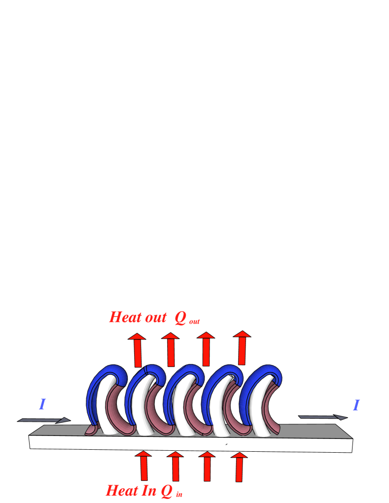
Whereas the currently available fabrication techniques of the graphene-based p-n junction are confined to surfaces, the three dimensional configurations of this flexible 2D membrane may eventually be exploited to develop integrated circuits with components not achievable before. In this paper, we show how a single, continuous graphene nanoribbon (GNR) may be used to create a nanoscale Peltier array without need for lithography or gating. The key ingredients in any Peltier cooler are an array of p-n junctions which are electrically in series yet thermally in parallel, such that the junctions which evolve heat are on one side of the device, and the junctions which absorb heat are on the other. Upon application of a current from left to right through the GNR shown in Fig. 1, heat will be pumped from the junctions near the bottom of the structure to the junctions near the top. From two different methods which agree, we estimate the cooling power of the proposed device to be on the order of .
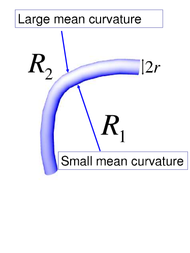
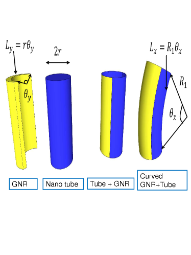
Curvature-induced doping provides a route to creating the p-n junctions required by Peltier coolers. When the local curvature of graphene resembles that of a sphere (large mean curvature), or that of a saddle (small mean curvature), the change in orbital energies and overlap integrals associated with the curvature causes the energy spectrums and the Dirac points to shift differently in these two cases, leading to n-type or p-type dopingkim2008 . By draping a single Armchair metallic GNR over a curved cylindrical protrusion (such as a bent nanotube may provide, see Fig. 22(b)), a region of large mean curvature is created next to a region of small mean curvature, and a p-n junction is created.
In Fig. 1, blue regions denote areas of large mean curvature and red regions denote areas of small mean curvature. The curvature-induced Dirac-point shift is given bykim2008
| (1) |
is the mean curvature of the surface at the point
| (2) |
where and are the principal radii of curvature at the point , is the nearest-neighbor distance, , and . In our proposed device, see Fig. 22(a), and for the outer surface while and for the inner surface. Because the Dirac-point shift depends on the square of kim2008 , it is independent of the coordinate system. The Dirac points in the regions with a larger magnitude of the mean curvature (locally like a sphere) are lowered more while the Dirac points in the regions with smaller magnitude of the mean curvature (regions which are flat, or alternatively which are saddle-like) are lowered less. This effect implies that regions with large magnitude of the mean curvature are locally electron-doped, while the regions with small magnitude of the mean curvature are locally hole-doped.
The optimal cooling power for one Peltier cooling element can be derived from the rate of heat absorptionrowe2006b
| (3) |
where is the temperature difference between the two heat reservoirs, , is the difference between Seebeck coefficients in the p-doped (with smaller mean curvature) and n-doped (with larger mean curvature) regions, and , the figure of merit of the p-n junction. and are the thermal conductance and electric resistance, respectively, of the p-n junction. When electrical current equal to is driven through one Peltier cooling element, the optimal cooling power is reached.
In the following, we use two approaches to estimate the cooling power of our proposed device under the condition that . For the first approach, we use Nonequilibrium Green’s Function (NEGF) method to perform calculations from the atomic scale. For the second approach, we estimate the cooling power from experimental measurements of the Seebeck coefficientwei2009 . Results from these two approaches are similar.
The NEGF method can be used to calculate the transmission coefficient for a perfect GNR from the atomic scaledatta2005b . The system contains one channel and two contacts. The Green’s function for the transport channel is defined as:
| (4) |
where is the incident energy of electrons, is the identity matrix with the same dimension as that of the channel Hamiltonian , is a small number accounting for the energy level broadening, and and represent the effects from two contacts. In order to describe the tunnelling processes between the channel and two contacts, two functions, and , are introduced for two contacts respectively,
| (5) |
The transmission coefficient for a perfect GNR is then given asdatta2005b
| (6) |
In real systems, scattering processes have to be taken into account. The electron-electron interaction usually causes phase relaxation, which destroys the coherence of the electronic wave functions. The electron-phonon interaction and the electron-impurity interaction result in backscattering and momentum relaxation processes. For high voltage bias between two contacts, effects from inelastic scatterings are also involved. Dominant scattering processes are determined by the physical system under consideration.
Under usual experimental conditions, where the voltage bias is small and the whole system is in the linear response regime, there is a way to take elastic scattering effects into account within NEGF. For quantum transport, it is well known that the transmission coefficient can be related to its ballistic limit counterpart in the following waydatta2005b ,
| (7) |
where is the system size along the transport direction and is the backscattering mean-free path and is assumed to depend only on disorder and not on the incident energy . Therefore, once is obtained, it is straightforward to calculate . For this paper, calculations of the the transmission coefficient are based on the GNR system with , , and .
After obtaining we can calculate the Seebeck coefficient and the electrical conductance . An intermediate function is defined asouyang2009
| (8) |
where is the Plank constant, and is the Fermi distribution function. Based on these intermediate functions, and can be computed as
| (9) |
| (10) |
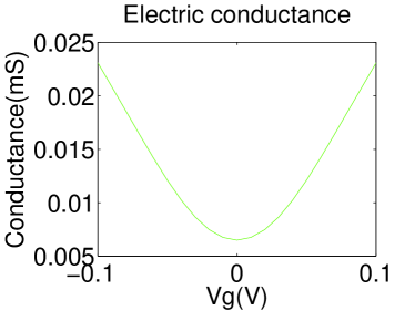
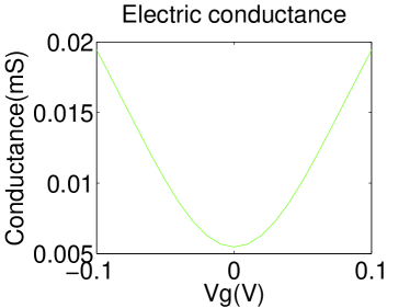
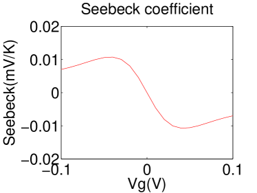
where is the electron charge, is the chemical potential and is the average temperature. In Fig.3, we show the electric conductance and the Seebeck coefficient at as functions of the on-site voltage for clean and disorder cases. We find that the electrical conductance of the clean case is slightly larger than that of the disordered case while the Seebeck coefficient behaves similarly in both cases. We furthermore find that the maximum of the Seebeck coefficient is on the order of , consistent with the experimental measurements for Graphenewei2009 .
The cooling power of our proposed device can be evaluated using the calculated Seebeck coefficient and electrical conductance with disorder. When the surface of a GNR is curved, Dirac points for different regions are shifted up or down, similar to applying a gate voltage. Therefore, the calculated Seebeck coefficient as a function of on-site voltage can be used as the Seebeck coefficients for different Dirac-point shifts caused by the curvatures. Combined with the calculated electric conductance, the cooling power can be calculated by using Eq.3 with .
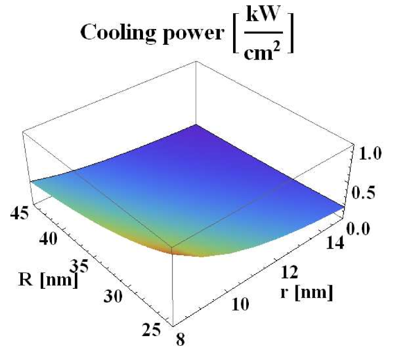
In Fig. 4, we show the cooling power as a function of two curvature radii and , where , , , and the distance between two nano tubes . and are fixed and . Therefore and have lower limits and , respectively. As we expect, the maximum cooling power takes place for small and , which is on the order of . As an example, if we take as inputs , , and , then the corresponding Dirac-point shifts for the inner side () and outer side () can be obtained after considering charge neutrality : , and . By using the calculated Seebeck coefficient and the electrical conductance (Fig. 33(d) and Fig. 33(b), respectively), we find that the cooling power is . When the cooling device is curved more, , the cooling power can be estimated in a similar way to be . This shows that the cooling power can be tuned by changing the curvature of the device, for example, by applying uniaxial pressure.

We now use an entirely different approach to estimate the cooling power of our proposed device, in which the Seebeck coefficients are taken directly from experimental measurements(Fig. 3(b) in ). Given the applied gate voltage , the resulting Dirac-point shift of the Graphene sample can be derived asnovoselov2004
| (11) |
where is the thickness of the substrate, is the Fermi velocity of graphene, and and are the permittivities of free space and , respectively. By using experimentally determined Seebeck coefficientwei2009 and electrical conductivitynovoselov2004 , the cooling power can be similarly estimated from Eq. 3.
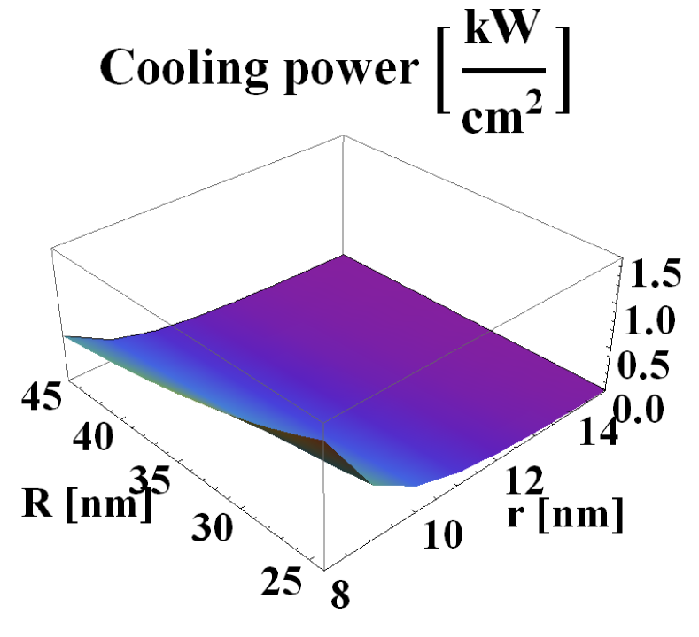
In Fig. 5, we report the cooling power as functions of the two curvature radii and as we do for the first approach. Results are consistent with that from the first approach, which is on the order of . As an example, if we take as inputs , , and , then the corresponding Dirac-point shifts for the inner side () and outer side () can be obtained: , and . This corresponds to applied gate voltages of , and . Given these two gate voltages, the Seebeck coefficients in both the n-type and p-type regionswei2009 can be obtained. Combined with experimental data for the electric conductance( , corresponding to the mobility ), the cooling power can be estimated to be . When the cooling device is curved more, , from similar calculations, the cooling power is obtained to be . This result again shows that we can tune the cooling power by bending the nanotubes through, e.g., applying uniaxial pressure.
In conclusion, we have proposed a graphene-based nano mechanical cooling device and estimated its cooling power using two different approaches: the NEGF method and experimental inputs. As a result of geometry alone, a series of P-N junctions are created in the proposed device such that by applying electric current, heat can be pumped perpendicular to the surface of the substrate. We find , close to that achievable with the best cooling devices chowdhury2009 . Most importantly, the cooling power of the proposed device can be adjusted by changing the curvatures, via, e.g., applying uniaxial pressure to the device.
Acknowledgements It is a pleasure to thank Y. Chen, E.-A. Kim, and Y. L. Loh for conversations. W. J. L. would like to thank Vinh Quang Diep and Seokmin Hong for many useful discussions. W. J. L., D. X. Y., and E. W. C. acknowledge support from Research Corporation for Science Advancement and NSF Grant No. DMR 11-06187 W. J. L. acknowledges support from the Purdue Research Foundation. D. X. Y. acknowledges support from NSFC-11074310, National Basic Research Program of China (No. 2012CB821400), and Research Fund for the Doctoral Program of Higher Education of China (20110171110026). EWC thanks École Supérieure de Physique et de Chimie Industrielles (ESPCI) for hospitality.
References
- (1) G. H. Zeng, X. F. Fan, C. LaBounty, E. Croke, Y. Zhang, J. Christofferson, D. Vashaee, A. Shakouri, and J. E. Bowers, Cooling power density of SiGe/Si superlattice micro refrigerators, volume 793 of Materials Research Society Symposium Proceedings, Materials Research Society, 2004.
- (2) I. Chowdhury, R. Prasher, K. Lofgreen, G. Chrysler, S. Narasimhan, R. Mahajan, D. Koester, R. Alley, and R. Venkatasubramanian, Nature Nanotechnology 4, 235 (2009).
- (3) X. Fan, G. Zeng, E. Croke, C. LaBounty, C. C. Ahn, D. Vashaee, A. Shakouri, and J. E. Bowers, Electronics letters 37, 126 (2001).
- (4) A. Shakouri and Y. Zhang, Ieee Transactions on Components and Packaging Technologies 28, 65 (2005).
- (5) J. Zhang, N. G. Anderson, and K. M. Lau, Applied Physics Letters 83, 374 (2003).
- (6) H.-Y. Chiu, V. Perebeinos, Y.-M. Lin, and P. Avouris, Nano Letters 10, 4634 (2010).
- (7) G. Liu, J. Velasco, Jairo, W. Bao, and C. N. Lau, Applied Physics Letters 92, 203103 (2008).
- (8) S.-G. Nam, D.-K. Ki, J. W. Park, Y. Kim, J. S. Kim, and H.-J. Lee, Nanotechnology 22, 415203 (2011).
- (9) B. Oezyilmaz, P. Jarillo-Herrero, D. Efetov, D. A. Abanin, L. S. Levitov, and P. Kim, Physical Review Letters 99, 166804 (2007).
- (10) G. Rao, M. Freitag, H.-Y. Chiu, R. S. Sundaram, and P. Avouris, Acs Nano 5, 5848 (2011).
- (11) J. R. Williams, L. DiCarlo, and C. M. Marcus, Science 317, 638 (2007).
- (12) T. Yu, C.-W. Liang, C. Kim, and B. Yu, Applied Physics Letters 98, 243105 (2011).
- (13) H.-C. Cheng, R.-J. Shiue, C.-C. Tsai, W.-H. Wang, and Y.-T. Chen, Acs Nano 5, 2051 (2011).
- (14) T. Lohmann, K. von Klitzing, and J. H. Smet, Nano Letters 9, 1973 (2009).
- (15) E. A. Kim and A. H. Castro Neto, Epl 84, 57007 (2008).
- (16) D. Rowe, Thermoelectrics handbook : macro to nano, Boca Raton : CRC/Taylor and Francis, 2006.
- (17) P. Wei, W. Z. Bao, Y. Pu, C. N. Lau, and J. Shi, Physical Review Letters 102, 166808 (2009).
- (18) S. Datta, Quantum transport : atom to transistor, Cambridge, UK ; Cambridge University Press, 2005.
- (19) Y. Ouyang and J. Guo, Applied Physics Letters 94, 263107 (2009).
- (20) K. S. Novoselov, A. K. Geim, S. V. Morozov, D. Jiang, Y. Zhang, S. V. Dubonos, I. V. Grigorieva, and A. A. Firsov, Science 306, 666 (2004).