Multifunctional Devices and Logic Gates With Undoped Silicon Nanowires
Abstract
We report on the electronic transport properties of multiple-gate devices fabricated from undoped silicon nanowires. Understanding and control of the relevant transport mechanisms was achieved by means of local electrostatic gating and temperature dependent measurements. The roles of the source/drain contacts and of the silicon channel could be independently evaluated and tuned. Wrap gates surrounding the silicide-silicon contact interfaces were proved to be effective in inducing a full suppression of the contact Schottky barriers, thereby enabling carrier injection down to liquid-helium temperature. By independently tuning the effective Schottky barrier heights, a variety of reconfigurable device functionalities could be obtained. In particular, the same nanowire device could be configured to work as a Schottky barrier transistor, a Schottky diode or a p-n diode with tunable polarities. This versatility was eventually exploited to realize a NAND logic gate with gain well above one.
Nanometer-scale electronic devices fabricated from silicon nanowires (SiNWs) are drawing significant attention in view of their potential application in electronics McAlpine et al. (2003), optoelectronics Yang et al. (2006) and biochemical sensing Cui and Lieber (2001); Patolsky et al. (2006). The transport properties and the functionality of such electronic devices are usually controlled by doping. In most cases, the incorporation of doping impurities in SiNWs is obtained in-situ during nanowire growth Yang et al. (2005), but a precise control over their spatial distribution Perea et al. (2009); Koren et al. (2010) and their activation Bjork et al. (2009) has not been achieved yet. Doping control becomes a particularly critical issue when the characteristic device size approaches the nanometer scale, i.e. comparable to the typical distance between dopants for standard doping levels ( - cm-3). In this limit, device performances can depend on only a few dopants Asenov et al. (2003); PierreM. et al. (2010), and be extremely sensitive to their precise locations, leading to a significant device-to-device variability. The main obstacle coming from the use of undoped nanowires lies in the difficulty to form low-resistance contacts due to the unavoidable presence of a Schottky barrier (SB) Tung (2001) at the metal-silicon interface. Therefore, understanding and controlling the properties of electrical contacts to SiNWs is of fundamental importance Leonard and Talin (2011). Here, we investigate the properties of metal-silicide contacts to undoped SiNWs, and we study the possibility to obtain largely-tunable contact resistances through a combination of two fabrication processes: a controlled silicidation of the metal-SiNW contacts and the fabrication of local gate electrodes wrapped around each silicon-silicide interface. We demonstrate that contact resistances can be largely suppressed with gate voltages of the order of 1 V, enabling measurable carrier injection down to 4K. In addition, through local electrostatic doping of the SiNW, our approach provides the possibility to implement different functionalities within the same SiNW device, which can work as a bipolar transistor, a Schottky diode or p-n diode with gate-tunable polarities. Finally, we provide as well an example of how two such devices could be programmed to operate as a NAND logic gate.
We used undoped SiNWs grown by chemical vapor deposition via a catalytic vapor-liquid-solid method (growth details were given in an earlier work Gentile et al. (2008)). Our sample fabrication process relies on a few steps of e-beam lithography, e-beam metal deposition, and lift-off. Initially, alignment markers and ordered arrays of 500-nm-wide Cr/Al (10/5 nm) gate electrodes, spaced by 500 nm, are defined on top of an oxidized heavily doped silicon substrate ( ). Successively, after a brief sonication in isopropanol, the as-grown undoped SiNWs are released from their growth substrate and drop-casted on the device substrate. Wires crossing a couple of bottom gates are identified by means of scanning electron microscopy (SEM) and contacted with 120-nm-thick nickel electrodes to be used as source and drain contacts. The bottom gates are also contacted in the same lithographic step. Prior to the Ni deposition, the native oxide on the SiNWs is etched away by dipping the sample for 5s in buffered HF. This step removes also the Al cap layer of the bottom gates leaving the underlying Cr layer unaffected. After contacting the SiNWs a double step thermal annealing process is performed in order to promote the silicidation of the contacts. Temperature and annealing times are calibrated in order obtain the protrusion of the nickel silicide along the nanowire Weber et al. (2006) from the Ni contacts to the bottom gates. The preparation of the sample is completed with the deposition of 80-nm-thick Al top gates overlapping with the bottom gates and, simultaneously, an additional top gate electrode crossing the middle region of the SiNW. The Al top gates are electrically isolated from the nanowire by a preliminary deposition and oxidation of four 1.5-nm-thick Al layers. Each layer is fully oxidized by leaving the sample in the load-lock chamber of the e-beam evaporator under an oxygen pressure of 200 Torr for 10 minutes. Due to their large overlapping area and to the small thickness of the (native) oxide interlayer, each bottom gate and the corresponding top gate are effectively shorted together, resulting in a wrap-gate geometry Storm et al. (2011).
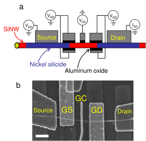
The SiNW device and its schematics are shown in 1. Since the nickel silicide sections have a metallic character, SB contacts are formed at the silicon-silicide interfaces. The wrap-gate electrodes, labelled as GS and GD, are designed to embed these interfaces and to control the respective SBs. We shall refer to these electrodes as to the contact gates. The wrap-gate geometry maximizes the gating efficiency. The finger-shape gate, labelled as GC, is meant to control carrier population in the channel. We shall refer to this electrode as to the channel gate.
The multiple gate layout enables independent control of the different device sections, i.e. the SB contacts and the channel. We shall begin by evaluating their relative contributions under different gating conditions and, for each case, we shall investigate the relevant transport mechanisms. At room temperature and for zero gate voltages, thermionic emission over the contact SBs is the dominant transport process. Since the Fermi level of the nickel silicide is pinned below the silicon mid-gap, i.e. closer to the valence band, transport across each silicide-silicon junction is dominated by the thermionic emission of holes over the p-type SB. The application of negative voltages to the contact-gates GS/GD produces a local band bending that reduces the thickness of the SB of the corresponding silicide-silicon junction. This enables the onset of thermally assisted tunneling through the barrier top-edge leading to a reduction of the effective p-type SB height Appenzeller et al. (2004a); Yang et al. (2008), . We find that negative contact-gate voltages of a few V are sufficient to induce a strong suppression of . This is apparent from 2(a) where the source-drain current, , is plotted as a function of the source-drain bias voltage, , for two gating conditions. The green characteristic corresponds to V and . In this case, the effective SB at the source contact is suppressed and the device behaves as a Schottky diode whose polarity is imposed by the SB at the drain contact. The blue characteristic corresponds to the reversed gating condition, i.e. V and , which results in an opposite diode polarity. In both cases the channel gate was set to V in order to get rid of any possible barrier in the channel (see discussion further below). Appreciable quantitative discrepancies can be noted in the two characteristics of 2(a). Under reverse-bias polarization, described by the qualitative band diagrams in the two insets of 2(a), the measured current is dominated by the thermally assisted tunneling of holes across the reverse-bias SB, i.e.
| (1) |
where eV/K is the Boltzmann constant, is the Richardson constant, is the temperature, is the absolute value of the electronic charge, is the cross-sectional area of the conducting silicon channel. From a ratio of between the reverse currents of the green and the blue characteristics, we estimate that the drain SB height exceeds the source SB height by .
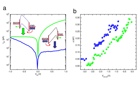
In order to independently measure the two effective SB heights and to study their gate-voltage dependence, the sample was loaded in a home-made variable-temperature insert. For each gate-voltage setting, temperature was varied between 220 K and 370 K in steps of 10 K. The effective barrier height was extracted from the temperature dependence of the reverse-bias current using the thermionic-emission relation (1) ( is given by the the slope of the Arrhenius plot vs ). The results are shown in 2(b), where the effective SB heights are plotted as a function of the corresponding contact-gate voltages. The two data sets reveal approximately linear gate-voltage dependences with same slopes. This denotes almost identical capacitive couplings to the respective contact gates. The drain SB height is 0.35 eV for and it vanishes for V. The source SB height for could not be directly measured due to the limited upper temperature of our setup. Yet a linear extrapolation of the data in 2(b) yields a source SB height of 0.45 eV for . This confirms the 0.1 eV difference with the drain SB height previously deduced from the ratio of the reverse currents in 2(a). Because of this difference, the source SB requires slightly more negative gate voltages to be entirely suppressed.
If both the effective SBs are simultaneously suppressed by sufficiently negative voltages applied to the respective contact gates, transport across the device becomes entirely dependent on the hole population of the silicon channel Appenzeller et al. (2004b). We find that current transport is dominated by the thermionic emission of holes over a potential barrier formed by the downward bending of the valence band edge. The emission of carriers over this barrier is purely thermionic as opposed to the case of the contact SBs where the onset of tunnelling leads to a smaller effective barrier. Following a similar procedure as before, we have measured the height of this barrier as a function of . The results are shown by solid dots in 3, where each dot is the result of a fit to an Arrhenius plot.
All data points were taken at constant V. A room-temperature characteristic, taken in the same range, is also shown on a logarithmic scale (red trace). The two data sets meet fairly well the proportionality relation expected from the thermionic-emission relation (1). The measured barrier height is eV for V and it decreases linearly for negative gate voltages. Below V, the barrier becomes too small to be reliably extracted from the Arrhenius plot (in this regime, transport is no longer thermally activated). A saturation of the characteristic is consistently observed below this threshold voltage.
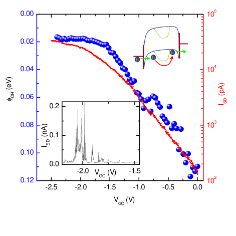
The complete suppression of the silicon-channel barrier, together with the suppression of the effective SBs at the silicon-silicide contacts, are further confirmed by low temperature measurements. An characteristic taken at K for V is shown in the lower inset of 3. While is unmeasurably small for V, pronounced current oscillations can be seen below this threshold, providing evidence of low-temperature transport through an undoped silicon device. The observed current oscillations are due to the Coulomb blockade effect. Their irregular structure reflects single-hole tunneling through a series of hole islands formed along the nanowire as it is typically observed in disordered low-dimensional conductors.
So far we have shown full control of hole transport in an undoped SiNW device. The same device could be operated as a p-type field-effect transistor, a Schottky diode, or a multi-island single-hole tunneling device. We pointed out that the p-type character of all these functionalities arises from the pinning of the silicide Fermi energy closer to the silicon valence band edge. At the same time, our thermionic-emission measurements revealed that the SB height can exhibit appreciable contact-to-contact variations within the same device. These variations can arise from the atomic structure of the silicide-silicon junction Gambino and Colgan (1998); Iwai et al. (2002); Morimoto et al. (1995); Murarka (1995); Bucher et al. (1986-06-01) as well as from the field effect of trapped charges in the periphery of the silicide-silicon junction Leonard and Talin (2011); Cai et al. (2012).
Given the relatively large variability ( eV) in the SB height of silicon-silicide contacts, it is possible to have SiNW devices where Fermi level pinning occurs close to the silicon mid-gap, yielding p-type and n-type SBs relatively close to each other and to the half-gap value (0.55 eV). These types of devices exhibit bipolar behavior and, as a result, they can give rise to a larger range of functionalities. 4(a) shows the bipolar field-effect characteristic of one of such devices with a gate layout identical to that of 1, except for the absence in this case of the channel-gate electrode. The horizontal axis refers to both contact-gate voltages being swept together.
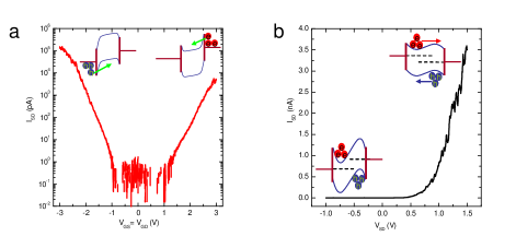
A more interesting behaviour is observed when the two gates are polarized at opposite voltages, fixed with respect to the corresponding (source or drain) contacts. 4(b) shows that, in this case, the device behaves like an electrostatically doped p-n diode. As opposed to the case of true diodes, here the built-in potential arises from static charges accumulated on the contact-gate electrodes Lee et al. (2004); Mueller et al. (2010); Heinzig et al. (2012); Martin et al. (2011) and not on the potential of the ionized impurities in the space-charge region. In the forward bias polarization the side of the nanowire populated with holes has a higher electrochemical potential than the side populated by electrons. The barriers created by the contact gate become smaller and can be surmounted by thermally activated carriers as shown in the upper inset of 4(b). This results in a diffusion current of holes from the p-like to the n-like region and an electron current in the opposite direction. In the case of reverse bias polarization, transport of electrons and holes is hindered by the high potential barriers created by the contact gates as depicted in the lower inset of 4(b).
Below we show that dual-gate SiNW devices, having Schottky contacts well coupled to the respective gates, can serve as building blocks for logic circuits. Bottom-up logic gates based on carbon nanotubes Bachtold et al. (2001); Derycke et al. (2001) or semiconductor nanowires Cui and Lieber (2001); Huang et al. (2001) have already been reported, along with more complex circuits like ring oscillators Chen et al. (2006) extending digital operation into the high frequency domain. Here we demonstrate the implementation of a NAND device made from two dual-gate SiNW devices connected in series as in 5(a). Since the SiNWs are undoped, this approach has the advantage of not requiring complementary doping. A NAND device performs an AND and a NOT operation in series. It accepts two input voltages corresponding to the binary values and and it delivers a single output voltage according to the truth table in 5(b). In our circuit, the voltage level V corresponds to a logical , while the voltage level V corresponds to a logical .
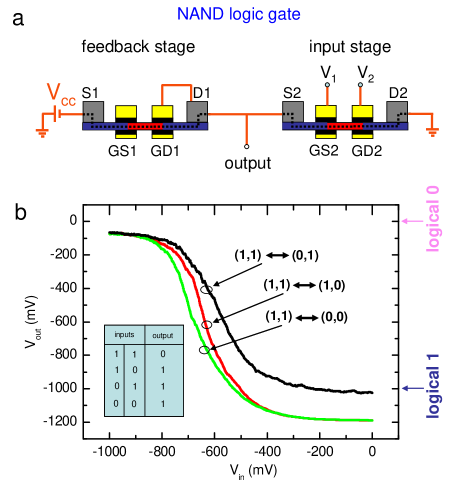
Let us now analyze the operating principle of this NAND device, by considering the different input configurations. When the two input gates controlling and are at logical , the input stage is in a highly resistive state due to both SBs being simultaneously high. As a consequence the bias voltage, V, falls mostly across the feedback stage and the output terminal acquires a value corresponding to a logical 1. The presence of an electrical connection between the output terminal and the contact gate produces a positive feedback, since a negative value on the contact gate suppresses the corresponding effective SB, making the impedance of the feedback stage lower and hence forcing even closer to , i.e. to logical output 1. When, on the contrary, both inputs are at logical , the input stage attains a low-resistive state due to the simultaneous suppression of both effective SBs. As a result, the output voltage approaches a logical 0, and falls mainly on the feeback stage. Because of the feedback line, V enforces a high value of the SB at the drain contact of the feedback stage. This increases its resistance with respect to the input stage, thereby reinforcing logical output 0. In the intermediate regimes, when one of the two inputs is at logical and the other is at logical , one gated SB is suppressed while the other is not. In this case, the presence of the feedback line is crucial in producing a stable configuration with , i.e. logical output 1. In fact, under this condition both of the effective SBs at the source and drain contacts of the feedback stage are suppressed leading to a lower impedance as compared to the input stage. As a result, the output voltage is stabilized at a logical 1.
Since in actual logic circuits the output of a logic gate can serve as the input of another gate, an important figure of merit for logic gates is gain, , defined as the slope of the linear portion of the output characteristic. A high-gain logic gate () has the capability to drive another logic gate without the need of signal restoration. From the data in 5(b) we find between and . In addition, the NAND gate requires relatively low voltage levels as compared to previously reported logic gates built from semiconductor nanowires Cui and Lieber (2001); Huang et al. (2001). Similar to other earlier worksBachtold et al. (2001), our NAND device was assembled from two dual-gate devices connected via external leads. Yet we should like to point out that the same logic gate could be obtained with a single nanowire using a common electrode for D1 and S2.
We thank the technical staff of the PTA cleanroom, G.Lapertot and C. Marin for their help in device fabrication and technical support. Massimo Mongillo gratefully acknowledges Antonella Orsino for useful discussions. This work was supported by the Agence Nationale de la Recherche (ANR) through the ACCESS and COHESION projects and by the European Commission through the Chemtronics program MEST-CT-2005-020513.
References
- McAlpine et al. (2003) M. C. McAlpine, R. S. Friedman, S. Jin, K.-h. Lin, W. U. Wang, and C. M. Lieber, Nano Letters 3, 1531 (2003), ISSN 1530-6984.
- Yang et al. (2006) C. Yang, C. J. Barrelet, F. Capasso, and C. M. Lieber, Nano Lett. 6, 2929 (2006), ISSN 1530-6984.
- Cui and Lieber (2001) Y. Cui and C. M. Lieber, Science 291, 851 (2001).
- Patolsky et al. (2006) F. Patolsky, B. P. Timko, G. Yu, Y. Fang, A. B. Greytak, G. Zheng, and C. M. Lieber, Science 313, 1100 (2006).
- Yang et al. (2005) C. Yang, Z. Zhong, and C. M. Lieber, Science 310, 1304 (2005).
- Perea et al. (2009) D. E. Perea, E. R. Hemesath, E. J. Schwalbach, J. L. Lensch-Falk, P. W. Voorhees, and L. J. Lauhon, Nat Nano 4, 315 (2009), ISSN 1748-3387.
- Koren et al. (2010) E. Koren, N. Berkovitch, and Y. Rosenwaks, Nano Lett. 10, 1163 (2010), ISSN 1530-6984.
- Bjork et al. (2009) M. T. Bjork, H. Schmid, J. Knoch, H. Riel, and W. Riess, Nat Nano 4, 103 (2009), ISSN 1748-3387.
- Asenov et al. (2003) A. Asenov, A. Brown, J. Davies, S. Kaya, and G. Slavcheva, Electron Devices, IEEE Transactions 50, 1837 (2003), ISSN 0018-9383.
- PierreM. et al. (2010) PierreM., WacquezR., JehlX., SanquerM., VinetM., and CuetoO., Nat Nano 5, 133 (2010).
- Tung (2001) R. T. Tung, Materials Science and Engineering: R: Reports 35, 1 (2001), ISSN 0927-796X.
- Leonard and Talin (2011) F. Leonard and A. A. Talin, Nat Nano 6, 773 (2011), ISSN 1748-3387.
- Gentile et al. (2008) P. Gentile, T. David, F. Dhalluin, D. Buttard, N. Pauc, M. Den Hertog, P. Ferret, and T. Baron, Nanotechnology 19, 125608 (2008), ISSN 0957-4484.
- Weber et al. (2006) W. M. Weber, L. Geelhaar, A. P. Graham, E. Unger, G. S. Duesberg, M. Liebau, W. Pamler, C. Cheze, H. Riechert, P. Lugli, et al., Nano Letters 6, 2660 (2006), ISSN 1530-6984.
- Storm et al. (2011) K. Storm, G. Nylund, L. Samuelson, and A. P. Micolich, Nano Lett. 12, 1 (2011), ISSN 1530-6984.
- Appenzeller et al. (2004a) J. Appenzeller, M. Radosavljevic , J. Knoch, and P. Avouris, Phys. Rev. Lett. 92, 048301 (2004a).
- Yang et al. (2008) W. Yang, S. Lee, G. Liang, R. Eswar, Z. Sun, and D. Kwong, Nanotechnology, IEEE Transactions on 7, 728 (2008), ISSN 1536-125X.
- Appenzeller et al. (2004b) J. Appenzeller, Y.-M. Lin, J. Knoch, and P. Avouris, Phys. Rev. Lett. 93, 196805 (2004b).
- Gambino and Colgan (1998) J. Gambino and E. Colgan, Materials Chemistry and Physics 52, 99 (1998), ISSN 0254-0584.
- Iwai et al. (2002) H. Iwai, T. Ohguro, and S.-i. Ohmi, Microelectronic Engineering 60, 157 (2002), ISSN 0167-9317.
- Morimoto et al. (1995) T. Morimoto, T. Ohguro, S. Momose, T. Iinuma, I. Kunishima, K. Suguro, I. Katakabe, H. Nakajima, M. Tsuchiaki, M. Ono, et al., Electron Devices, IEEE Transactions on 42, 915 (1995), ISSN 0018-9383.
- Murarka (1995) S. P. Murarka, Intermetallics 3, 173 (1995), ISSN 0966-9795.
- Bucher et al. (1986-06-01) E. Bucher, S. Schulz, M. C. Lux-Steiner, P. Munz, U. Gubler, and F. Greuter, Work function and barrier heights of transition metal silicides (1986-06-01).
- Cai et al. (2012) W. Cai, Y. Che, J. P. Pelz, E. R. Hemesath, and L. J. Lauhon, Nano Lett. 12, 694 (2012), ISSN 1530-6984.
- Lee et al. (2004) J. U. Lee, P. P. Gipp, and C. M. Heller, Appl. Phys. Lett. 85, 145 (2004).
- Mueller et al. (2010) T. Mueller, M. Kinoshita, M. Steiner, V. Perebeinos, A. A. Bol, D. B. Farmer, and P. Avouris, Nat Nano 5, 27 (2010), ISSN 1748-3387.
- Heinzig et al. (2012) A. Heinzig, S. Slesazeck, F. Kreupl, T. Mikolajick, and W. M. Weber, Nano Lett. 12, 119 (2012), ISSN 1530-6984.
- Martin et al. (2011) D. Martin, A. Heinzig, M. Grube, L. Geelhaar, T. Mikolajick, H. Riechert, and W. M. Weber, Phys. Rev. Lett. 107, 216807 (2011).
- Bachtold et al. (2001) A. Bachtold, P. Hadley, T. Nakanishi, and C. Dekker, Science 294, 1317 (2001).
- Derycke et al. (2001) V. Derycke, R. Martel, J. Appenzeller, and P. Avouris, Nano Letters 1, 453 (2001), ISSN 1530-6984.
- Huang et al. (2001) Y. Huang, X. Duan, Y. Cui, L. J. Lauhon, K.-H. Kim, and C. M. Lieber, Science 294, 1313 (2001).
- Chen et al. (2006) Z. Chen, J. Appenzeller, Y.-M. Lin, J. Sippel-Oakley, A. G. Rinzler, J. Tang, S. J. Wind, P. M. Solomon, and P. Avouris, Science 311, 1735 (2006).